EP0890983A1 - Motif de circuit et méthode pour mesurer la précision dimensionnelle ainsi que le revêtement d'un motif de circuit - Google Patents
Motif de circuit et méthode pour mesurer la précision dimensionnelle ainsi que le revêtement d'un motif de circuit Download PDFInfo
- Publication number
- EP0890983A1 EP0890983A1 EP97310515A EP97310515A EP0890983A1 EP 0890983 A1 EP0890983 A1 EP 0890983A1 EP 97310515 A EP97310515 A EP 97310515A EP 97310515 A EP97310515 A EP 97310515A EP 0890983 A1 EP0890983 A1 EP 0890983A1
- Authority
- EP
- European Patent Office
- Prior art keywords
- pattern
- accuracy
- measurement
- patterns
- overlay
- Prior art date
- Legal status (The legal status is an assumption and is not a legal conclusion. Google has not performed a legal analysis and makes no representation as to the accuracy of the status listed.)
- Withdrawn
Links
Images


Classifications
-
- G—PHYSICS
- G03—PHOTOGRAPHY; CINEMATOGRAPHY; ANALOGOUS TECHNIQUES USING WAVES OTHER THAN OPTICAL WAVES; ELECTROGRAPHY; HOLOGRAPHY
- G03F—PHOTOMECHANICAL PRODUCTION OF TEXTURED OR PATTERNED SURFACES, e.g. FOR PRINTING, FOR PROCESSING OF SEMICONDUCTOR DEVICES; MATERIALS THEREFOR; ORIGINALS THEREFOR; APPARATUS SPECIALLY ADAPTED THEREFOR
- G03F7/00—Photomechanical, e.g. photolithographic, production of textured or patterned surfaces, e.g. printing surfaces; Materials therefor, e.g. comprising photoresists; Apparatus specially adapted therefor
- G03F7/70—Microphotolithographic exposure; Apparatus therefor
- G03F7/70483—Information management; Active and passive control; Testing; Wafer monitoring, e.g. pattern monitoring
- G03F7/70605—Workpiece metrology
- G03F7/70616—Monitoring the printed patterns
- G03F7/70633—Overlay, i.e. relative alignment between patterns printed by separate exposures in different layers, or in the same layer in multiple exposures or stitching
-
- G—PHYSICS
- G03—PHOTOGRAPHY; CINEMATOGRAPHY; ANALOGOUS TECHNIQUES USING WAVES OTHER THAN OPTICAL WAVES; ELECTROGRAPHY; HOLOGRAPHY
- G03F—PHOTOMECHANICAL PRODUCTION OF TEXTURED OR PATTERNED SURFACES, e.g. FOR PRINTING, FOR PROCESSING OF SEMICONDUCTOR DEVICES; MATERIALS THEREFOR; ORIGINALS THEREFOR; APPARATUS SPECIALLY ADAPTED THEREFOR
- G03F7/00—Photomechanical, e.g. photolithographic, production of textured or patterned surfaces, e.g. printing surfaces; Materials therefor, e.g. comprising photoresists; Apparatus specially adapted therefor
- G03F7/70—Microphotolithographic exposure; Apparatus therefor
- G03F7/70483—Information management; Active and passive control; Testing; Wafer monitoring, e.g. pattern monitoring
- G03F7/70605—Workpiece metrology
- G03F7/70616—Monitoring the printed patterns
- G03F7/70625—Dimensions, e.g. line width, critical dimension [CD], profile, sidewall angle or edge roughness
-
- G—PHYSICS
- G03—PHOTOGRAPHY; CINEMATOGRAPHY; ANALOGOUS TECHNIQUES USING WAVES OTHER THAN OPTICAL WAVES; ELECTROGRAPHY; HOLOGRAPHY
- G03F—PHOTOMECHANICAL PRODUCTION OF TEXTURED OR PATTERNED SURFACES, e.g. FOR PRINTING, FOR PROCESSING OF SEMICONDUCTOR DEVICES; MATERIALS THEREFOR; ORIGINALS THEREFOR; APPARATUS SPECIALLY ADAPTED THEREFOR
- G03F7/00—Photomechanical, e.g. photolithographic, production of textured or patterned surfaces, e.g. printing surfaces; Materials therefor, e.g. comprising photoresists; Apparatus specially adapted therefor
- G03F7/70—Microphotolithographic exposure; Apparatus therefor
- G03F7/70483—Information management; Active and passive control; Testing; Wafer monitoring, e.g. pattern monitoring
- G03F7/70605—Workpiece metrology
- G03F7/70681—Metrology strategies
- G03F7/70683—Mark designs
-
- G—PHYSICS
- G03—PHOTOGRAPHY; CINEMATOGRAPHY; ANALOGOUS TECHNIQUES USING WAVES OTHER THAN OPTICAL WAVES; ELECTROGRAPHY; HOLOGRAPHY
- G03F—PHOTOMECHANICAL PRODUCTION OF TEXTURED OR PATTERNED SURFACES, e.g. FOR PRINTING, FOR PROCESSING OF SEMICONDUCTOR DEVICES; MATERIALS THEREFOR; ORIGINALS THEREFOR; APPARATUS SPECIALLY ADAPTED THEREFOR
- G03F7/00—Photomechanical, e.g. photolithographic, production of textured or patterned surfaces, e.g. printing surfaces; Materials therefor, e.g. comprising photoresists; Apparatus specially adapted therefor
- G03F7/70—Microphotolithographic exposure; Apparatus therefor
- G03F7/70483—Information management; Active and passive control; Testing; Wafer monitoring, e.g. pattern monitoring
- G03F7/70605—Workpiece metrology
- G03F7/706835—Metrology information management or control
-
- G—PHYSICS
- G03—PHOTOGRAPHY; CINEMATOGRAPHY; ANALOGOUS TECHNIQUES USING WAVES OTHER THAN OPTICAL WAVES; ELECTROGRAPHY; HOLOGRAPHY
- G03F—PHOTOMECHANICAL PRODUCTION OF TEXTURED OR PATTERNED SURFACES, e.g. FOR PRINTING, FOR PROCESSING OF SEMICONDUCTOR DEVICES; MATERIALS THEREFOR; ORIGINALS THEREFOR; APPARATUS SPECIALLY ADAPTED THEREFOR
- G03F7/00—Photomechanical, e.g. photolithographic, production of textured or patterned surfaces, e.g. printing surfaces; Materials therefor, e.g. comprising photoresists; Apparatus specially adapted therefor
- G03F7/70—Microphotolithographic exposure; Apparatus therefor
- G03F7/70483—Information management; Active and passive control; Testing; Wafer monitoring, e.g. pattern monitoring
- G03F7/70605—Workpiece metrology
- G03F7/706843—Metrology apparatus
- G03F7/706845—Calibration, e.g. tool-to-tool calibration, beam alignment, spot position or focus
-
- G—PHYSICS
- G03—PHOTOGRAPHY; CINEMATOGRAPHY; ANALOGOUS TECHNIQUES USING WAVES OTHER THAN OPTICAL WAVES; ELECTROGRAPHY; HOLOGRAPHY
- G03F—PHOTOMECHANICAL PRODUCTION OF TEXTURED OR PATTERNED SURFACES, e.g. FOR PRINTING, FOR PROCESSING OF SEMICONDUCTOR DEVICES; MATERIALS THEREFOR; ORIGINALS THEREFOR; APPARATUS SPECIALLY ADAPTED THEREFOR
- G03F9/00—Registration or positioning of originals, masks, frames, photographic sheets or textured or patterned surfaces, e.g. automatically
- G03F9/70—Registration or positioning of originals, masks, frames, photographic sheets or textured or patterned surfaces, e.g. automatically for microlithography
- G03F9/7003—Alignment type or strategy, e.g. leveling, global alignment
- G03F9/7007—Alignment other than original with workpiece
- G03F9/7015—Reference, i.e. alignment of original or workpiece with respect to a reference not on the original or workpiece
-
- G—PHYSICS
- G03—PHOTOGRAPHY; CINEMATOGRAPHY; ANALOGOUS TECHNIQUES USING WAVES OTHER THAN OPTICAL WAVES; ELECTROGRAPHY; HOLOGRAPHY
- G03F—PHOTOMECHANICAL PRODUCTION OF TEXTURED OR PATTERNED SURFACES, e.g. FOR PRINTING, FOR PROCESSING OF SEMICONDUCTOR DEVICES; MATERIALS THEREFOR; ORIGINALS THEREFOR; APPARATUS SPECIALLY ADAPTED THEREFOR
- G03F9/00—Registration or positioning of originals, masks, frames, photographic sheets or textured or patterned surfaces, e.g. automatically
- G03F9/70—Registration or positioning of originals, masks, frames, photographic sheets or textured or patterned surfaces, e.g. automatically for microlithography
- G03F9/7073—Alignment marks and their environment
- G03F9/7076—Mark details, e.g. phase grating mark, temporary mark
-
- G—PHYSICS
- G03—PHOTOGRAPHY; CINEMATOGRAPHY; ANALOGOUS TECHNIQUES USING WAVES OTHER THAN OPTICAL WAVES; ELECTROGRAPHY; HOLOGRAPHY
- G03F—PHOTOMECHANICAL PRODUCTION OF TEXTURED OR PATTERNED SURFACES, e.g. FOR PRINTING, FOR PROCESSING OF SEMICONDUCTOR DEVICES; MATERIALS THEREFOR; ORIGINALS THEREFOR; APPARATUS SPECIALLY ADAPTED THEREFOR
- G03F9/00—Registration or positioning of originals, masks, frames, photographic sheets or textured or patterned surfaces, e.g. automatically
- G03F9/70—Registration or positioning of originals, masks, frames, photographic sheets or textured or patterned surfaces, e.g. automatically for microlithography
- G03F9/7073—Alignment marks and their environment
- G03F9/708—Mark formation
-
- H—ELECTRICITY
- H10—SEMICONDUCTOR DEVICES; ELECTRIC SOLID-STATE DEVICES NOT OTHERWISE PROVIDED FOR
- H10P—GENERIC PROCESSES OR APPARATUS FOR THE MANUFACTURE OR TREATMENT OF DEVICES COVERED BY CLASS H10
- H10P74/00—Testing or measuring during manufacture or treatment of wafers, substrates or devices
- H10P74/27—Structural arrangements therefor
-
- H—ELECTRICITY
- H10—SEMICONDUCTOR DEVICES; ELECTRIC SOLID-STATE DEVICES NOT OTHERWISE PROVIDED FOR
- H10W—GENERIC PACKAGES, INTERCONNECTIONS, CONNECTORS OR OTHER CONSTRUCTIONAL DETAILS OF DEVICES COVERED BY CLASS H10
- H10W46/00—Marks applied to devices, e.g. for alignment or identification
-
- H—ELECTRICITY
- H10—SEMICONDUCTOR DEVICES; ELECTRIC SOLID-STATE DEVICES NOT OTHERWISE PROVIDED FOR
- H10W—GENERIC PACKAGES, INTERCONNECTIONS, CONNECTORS OR OTHER CONSTRUCTIONAL DETAILS OF DEVICES COVERED BY CLASS H10
- H10W46/00—Marks applied to devices, e.g. for alignment or identification
- H10W46/301—Marks applied to devices, e.g. for alignment or identification for alignment
-
- H—ELECTRICITY
- H10—SEMICONDUCTOR DEVICES; ELECTRIC SOLID-STATE DEVICES NOT OTHERWISE PROVIDED FOR
- H10P—GENERIC PROCESSES OR APPARATUS FOR THE MANUFACTURE OR TREATMENT OF DEVICES COVERED BY CLASS H10
- H10P74/00—Testing or measuring during manufacture or treatment of wafers, substrates or devices
- H10P74/20—Testing or measuring during manufacture or treatment of wafers, substrates or devices characterised by the properties tested or measured, e.g. structural or electrical properties
- H10P74/203—Structural properties, e.g. testing or measuring thicknesses, line widths, warpage, bond strengths or physical defects
Definitions
- the present invention relates to a photolithography process in semiconductor apparatus fabrication. And more particularly, to a measurement pattern set and a method for measuring dimension accuracy and overlay accuracy of a circuit pattern, which is transferred onto a substrate surface.
- photolithography processes are important to improve quality of the semiconductor integrated circuit.
- Such photolithography processes are performed using a projection aligner.
- a circuit pattern formed on a reticle is repeatedly transferred onto a semiconductor substrate, such as wafer, using the projection aligner.
- the transferred circuit pattern on the wafer is measured in size relative to design requirement, and overlay accuracy relative to a pattern in the under layer is measured as well.
- the circuit pattern is provided with a measurement pattern, which is specialized for pattern measurement.
- a measurement pattern is detected by a specialized measurement device, and the measured size is compared to its design value to provide a dimension error of the circuit pattern.
- the circuit pattern is decided whether to be in a predetermined allowable range of dimension accuracy standard. When the dimension error is within the dimension accuracy standard, the circuit pattern is acceptable. On the other hand, the dimension error of the circuit pattern is out of the standard, the chip including the unacceptable circuit pattern is rejected as a defective product.
- another specialized measurement pattern is used for detecting the position of the circuit pattern relative to the pattern on the lower layer.
- another specialized measurement pattern is formed as well.
- Those two measurement patterns on the top and lower layer are detected by an overlay measurement device.
- the difference in position between the two specialized measurement patterns on the top and lower layers is compared to an overlay accuracy standard.
- the wafer shifts to the next process.
- an object of the invention is to provide a measurement pattern set, with which dimension accuracy and overlay accuracy of a circuit pattern can be decided easily in a short time.
- Another object of the invention is to provide a method for measuring dimension accuracy and overlay accuracy of a circuit pattern, by which the dimension accuracy and overlay accuracy of the circuit pattern can be decided easily in a short time.
- Still another object of the invention is to provide an apparatus for measuring dimension accuracy and overlay accuracy of a circuit pattern, by which the dimension accuracy and overlay accuracy of the circuit pattern can be decided easily with simple structure.
- a measurement pattern set according to a first aspect of the invention includes a first pattern formed on a lower layer, which is to be the basis of the measurement; and a second pattern formed on an upper layer that is the same level of the circuit pattern.
- the second pattern is arranged to adjoin to the first pattern.
- the first and second patterns are measured in size so as to calculate a dimension error of the second pattern relative to its design value and an overlay error of the second pattern relative to the first pattern at the same time.
- the dimension accuracy and overlay accuracy of the circuit pattern is calculated in response to the above calculated dimension error and the overlay error.
- a first pattern is formed on a lower layer, which is to be the basis of the measurement.
- a second pattern is formed on an upper layer that is the same level of the circuit pattern, in which the second pattern is arranged to adjoin to the first pattern.
- sizes of the first and second patterns are measured so as to calculate a dimension error of the second pattern relative to its design value and an overlay error of the second pattern relative to the first pattern at the same time.
- the dimension accuracy and overlay accuracy of the circuit pattern is calculated in response to the above calculated dimension error and the overlay error.
- An apparatus includes a measurement device that measures sizes of first and second patterns at the same time.
- the first pattern is formed on a lower layer and the second pattern is formed on an upper layer that is the same level of the circuit pattern.
- the apparatus further includes a calculation unit that calculates a dimension error of the second pattern relative to its design value and an overlay error of the second pattern relative to the first pattern at the same time, and sums up the dimension error and the overlay error.
- the apparatus is also provided with a decision unit that compares the sum of the dimension error and overlay error of the second pattern to a predetermined reference value to decide whether the total pattern quality of the circuit pattern is in a standard range or not.
- the dimension accuracy and overlay accuracy of the circuit pattern can be decided with a single measurement device.
- each of the first and second patterns may be designed so that sizes both in X and Y directions are measured at the same time.
- the patterns can be measured in size both in X and Y directions at the same time, and the pattern quality of the circuit pattern can be decided for each direction independently.
- the first pattern may include a pair of line patterns which extend in the X and Y directions on the difference layers, respectively.
- the pattern quality of the circuit pattern can be decided relative to the different layers for each direction independently.
- the first pattern may include a pair of line patterns which are arranged at both sides of a line extending in the X direction on two different layers, respectively; and another pair of line patterns which are arranged at both sides of a line extending in the Y direction on another two different layers, respectively, so that the overlay accuracy is measured relative to each of those four different layers.
- the pattern quality of the circuit pattern can be decided relative to two different processes (layers) in X direction, and it can be decided relative to another two different processes (layers) in Y direction, as well. Namely, the pattern quality can be decided relative to four different processes (layers).
- Fig. 1 an apparatus for measuring dimension accuracy and overlay accuracy of a circuit pattern (not shown) transferred onto a wafer 2, which is placed on a wafer stage 4.
- the apparatus includes a photo-detector 6, a calculation unit 7 connected to the photo-detector 6, and a decision unit 8 connected to the calculation unit 7.
- the photo-detector 6 includes an image sensor in which charges are introduced when light from a chip region of the wafer 2 is focused on the surface thereof. Namely, the photo-detector 6 detects first and second measurement patterns (11 and 12) transferred on a chip region of the wafer 2 to measure sizes ("a,” "b” and "c") of those patterns at the same time. In each chip region on the wafer 2, a plurality of circuit patterns are transferred one over another.
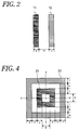
- Fig. 2 shows a measurement pattern set, transferred onto the surface of the wafer 2, according to a first embodiment of the invention.
- the measurement pattern set includes the first line pattern 11 and the second line pattern 12, which may be transferred outside the circuit pattern in the chip region.
- the first line pattern 11 is an etching pattern formed on a lower layer (reference layer), which is to be the basis of overlay accuracy measurement.
- the second line pattern 12 is a resist pattern formed on an upper layer, overlapped on the lower layer.
- the first and second line patterns 11 and 12 are arranged at adjacent locations to each other.
- the calculation unit 7 calculates a dimension error of the second measurement pattern 12 relative to its design value and an overlay error of the second measurement pattern 12 relative to the first measurement pattern 11 at the same time.
- the calculation unit 7 also sums up the dimension error and the overlay error.
- the decision unit 8 compares the sum of the dimension error and overlay error, supplied from the calculation unit 7, to a predetermined reference value to decide whether the total pattern quality of the circuit pattern is in a standard range or not.
- the first line pattern 11 is a pattern specialized for size measurement, which is designed to have a size (width) "a.”
- the second line pattern 12 is a pattern specialized for size measurement, which is designed to have a size (width) "c,” as well.
- the first and second line patterns 11 and 12 are arranged to have a distance "b" so that no problem occurs in the formation thereof.
- the distance "b" between the line patterns 11 and 12 is arbitrarily designed.
- the above mentioned sizes "a,” b” and “c” may be 0.5 ⁇ m, 1 ⁇ m and 0.5 ⁇ m, respectively.
- the size "a" of the first line pattern 11, the distance "b” between the line patterns 11 and 12 and the size "c" of the second line pattern 12 are measured by the photo detector 6, shown in Fig. 1.
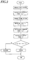
- Fig. 3 shows the steps for deciding dimension accuracy and overlay accuracy of the circuit pattern.
- the calculation unit 7 decides the accuracy of the circuit pattern on the basis of the above measured values "a,” "b” and "c" as follows:
- the size "a" of the first line pattern 11 has been measured before the second line pattern 12 is formed, and the size is always in the allowable range. It is assumed that a dimension error of the first line pattern 11 relative to its design value is ⁇ a'.
- the overlay accuracy is decided in accordance with the following formula: B ⁇ a' + ⁇ c + A where "B" is the standard range of overlay accuracy When it meets the above formula, the circuit pattern is decided to be acceptable.
- the first and second line patterns 11 and 12 are measured in size at the same time, so that the dimension accuracy and overlay accuracy of the circuit pattern can be decided with a single measurement device (6, 7 and 8).
- Fig. 4 shows a measurement pattern set, transferred onto the surface of the wafer 2, according to a second preferred embodiment of the invention.
- the measurement pattern set includes a first measurement pattern 21, formed on a lower layer (reference layer), and a second measurement pattern 12, formed on an upper layer.
- the lower layer is to be the basis of overlay accuracy measurement of the upper layer.
- Each of the first and second measurement patterns 21 and 22 is shaped to be a square frame.
- the second measurement pattern 22 is arranged to surround the first measurement pattern 21 at the center.
- the first measurement pattern 21 is designed to have frame widths of "c,” “d,” “i” and “j,” which are appropriate for size control, and to have lengths that are long enough to measure the sizes "c,” “d,” “i” and “j.”
- the frame widths "c,” “d,” “i” and “j” of the first measurement pattern 21 are designed to be appropriate, not too large nor too small, so that the sizes are close to those of the circuit pattern formed on the same layer (upper layer).
- the second measurement pattern 22 is formed in the same manner as the first embodiment.
- the second measurement pattern 22 is a resist pattern, which is designed to have frame widths of "a,” “f,” “g” and “l” to provide a size target.
- the frame widths "a,” “f,” “g,' and “l” of the second measurement pattern 21 are designed to be appropriate, not too large nor too small, so that the sizes are close to those of the circuit pattern formed on the same layer (upper layer).
- the first and second measurement patterns 21 and 22 are arranged to have arbitrary distances "b,” “e,” “h” and “k” so that the second measurement pattern 22 can be formed without any effect of the first measurement pattern 21.
- the first measurement pattern 21 is designed to have an inner width D of 1 to 2 ⁇ m.
- first, every size of thus formed first and second measurement patterns 21 and 22 is measured.
- the horizontal direction is X and the vertical direction is Y. Every size of the first and second measurement patterns 21 and 22 arranged within an area of X-X' and Y-Y' is measured in a single plane at the same time.
- measurement of the second measurement pattern 22 in the Y direction is performed.
- measurement can be performed both in the X and Y directions at the same time, and therefore, pattern accuracy data of the circuit pattern can be provided in each direction independently.
- size data are taken from both right and left sides of the pattern, size data only at one of those sides can be used for deciding the pattern accuracy with the same advantage.
- the measurement of the patterns 21 and 22, calculation process of dimension error and overlay error, and decision process of pattern quality of the circuit pattern are performed by the apparatus, shown in Fig. 1, in the same manner as the first preferred embodiment.
- every size of the first and second measurement patterns 21 and 22 can be measured both in X and Y directions at the same time, and therefore, the pattern quality of the circuit pattern can be decided for each direction easily.
- Fig. 5 shows a measurement pattern set, transferred onto the surface of the wafer 2, according to a third preferred embodiment of the invention.
- overlay accuracy of a circuit pattern is decided using different reference layers for X and Y directions, respectively.
- the measurement pattern set includes a first pair of measurement patterns 31, a second pair of measurement patterns 32 and a third measurement pattern 33.
- the first pair of measurement patterns 31 are designed to extend in a Y direction
- the second pair of measurement patterns 32 are designed to extend in an X direction.
- the third measurement pattern 33 is shaped to be a square frame.
- the first and second pairs of measurement patterns 31 and 32 are formed on a first layer, which is the lowest, and on a second layer, which is on the first layer, respectively.
- the third layer 33 is formed on the top layer, on which the circuit pattern is transferred as well.
- the first pair of measurement patterns 31 are formed in the same manner as the patterns described in the first and second preferred embodiments.
- a dimension error ⁇ 31x of the measurement patterns 31 relative to its design value a dimension error ⁇ 33x of the measurement patterns 33 relative to its design value and an overlay error ⁇ x between the measurement patterns 31 and 33 are calculated.
- pattern accuracy of the circuit pattern is decided in the X direction: x ⁇ ⁇ 31x+ ⁇ x+ ⁇ 33x where "x" is a predetermined range of total accuracy standard of the circuit pattern.
- the first and second pairs of measurement patterns 31 and 32 are formed in the different layers, so that the overlay accuracy of the circuit pattern on the top layer can be decided relative to two different layers independently.
- the measurement of the patterns 31 to 33, calculation process of dimension error and overlay error, and decision process of pattern quality of the circuit pattern are performed by the apparatus, shown in Fig. 1, in the same manner as the first preferred embodiment.
- every size of the measurement patterns 31 to 33 can be measured both in X and Y directions at the same time, and the pattern accuracy of the circuit pattern can be decided relative to the different layers for each direction easily.
- Fig. 6 shows a measurement pattern set, transferred onto the surface of the wafer 2, according to a fourth preferred embodiment of the invention.
- overlay accuracy of a circuit pattern is decided relative to two different layers in each direction of X and Y.
- the measurement pattern set includes first to fifth measurement patterns 41 to 45.
- the first and second measurement patterns 41 and 42 are designed to extend in the Y direction, at the right and left sides of a line Y-Y', respectively.
- the third and fourth measurement patterns 43 and 44 are designed to extend in the X direction, at the upper and lower sides of a line X-X', respectively.
- the fifth measurement pattern 45 is shaped to be a square frame, surrounded by the first to fourth measurement patterns 41 to 44.
- the first to fifth measurement patterns 41 to 45 are formed on different layers in order lowest to top.
- the circuit pattern is formed on the top layer with the fifth measurement pattern 45.
- the first and second measurement layers 41 and 42 are used for measuring overlay accuracy of the circuit pattern in the X direction.
- the third and fourth measurement layers 43 and 44 are used for measuring overlay accuracy of the circuit pattern in the Y direction.
- the measurement patterns 41 to 45 For measuring the measurement patterns 41 to 45, first, every size in the X direction (X-X') is measured. A dimension error ⁇ a of the first measurement pattern 41 relative to its design value and a dimension error ⁇ f of the second measurement pattern 42 relative to its design value are obtained in advance when those patterns are formed. In accordance with the result of the measurement in the X direction, the average of sizes "c" and "d" of the fifth measurement pattern 45 is calculated, and then a dimension error ⁇ 45 of the fifth measurement pattern 45 is calculated relative to its design value.
- the total accuracy of the pattern 45 relative to the pattern 41 means the pattern quality of the circuit pattern formed on the top layer relative to the lowest layer, on which the first measurement pattern 41 is formed.
- the total accuracy of the fifth measurement pattern 45 relative to the second measurement pattern 42 is decided in accordance with the following formula: x2 ⁇ f + ⁇ (42-45) + ⁇ 45 where " ⁇ e" is an allowable range of accuracy standard.
- the total accuracy of the pattern 45 relative to the pattern 42 means the pattern quality of the circuit pattern formed on the top layer relative to the lower layer, on which the second measurement pattern 42 is formed.
- a dimension error of each of the measurement patterns 43, 44 and 45 is measured, and overlay accuracy of the fifth measurement pattern 45 relative to the third and fourth measurement patterns 43 and 44 is measured, respectively.
- a pattern quality of the circuit pattern can be decided.
- the measurement of the patterns 41 to 45, calculation process of dimension error and overlay error, and decision process of pattern quality of the circuit pattern are performed by the apparatus, shown in Fig. 1, in the same manner as the first preferred embodiment.
- the pattern quality of the circuit pattern can be decided relative to two different processes (layers) in the X direction, and it can be decided relative to another two different processes (layers) in the Y direction, as well.
- the measurement patterns can be measured both in X and Y directions at the same time, and the pattern quality of the circuit pattern can be decided relative to four different processes (layers). If other patterns are formed outside the measurement patterns 41 and 42, the number of processes relative to which the pattern quality is decided can be increased.
Landscapes
- Physics & Mathematics (AREA)
- General Physics & Mathematics (AREA)
- Exposure And Positioning Against Photoresist Photosensitive Materials (AREA)
- Testing Or Measuring Of Semiconductors Or The Like (AREA)
- Exposure Of Semiconductors, Excluding Electron Or Ion Beam Exposure (AREA)
- Length Measuring Devices By Optical Means (AREA)
Applications Claiming Priority (2)
| Application Number | Priority Date | Filing Date | Title |
|---|---|---|---|
| JP186954/97 | 1997-07-11 | ||
| JP9186954A JPH1131649A (ja) | 1997-07-11 | 1997-07-11 | パターン寸法と重ね合わせ精度の測定パターン及びその測定方法 |
Publications (1)
| Publication Number | Publication Date |
|---|---|
| EP0890983A1 true EP0890983A1 (fr) | 1999-01-13 |
Family
ID=16197640
Family Applications (1)
| Application Number | Title | Priority Date | Filing Date |
|---|---|---|---|
| EP97310515A Withdrawn EP0890983A1 (fr) | 1997-07-11 | 1997-12-23 | Motif de circuit et méthode pour mesurer la précision dimensionnelle ainsi que le revêtement d'un motif de circuit |
Country Status (3)
| Country | Link |
|---|---|
| EP (1) | EP0890983A1 (fr) |
| JP (1) | JPH1131649A (fr) |
| KR (1) | KR19990013281A (fr) |
Cited By (4)
| Publication number | Priority date | Publication date | Assignee | Title |
|---|---|---|---|---|
| WO2003003122A2 (fr) | 2001-06-29 | 2003-01-09 | Infineon Technologies Ag | Procede de mesure de recouvrement et de dimension critique combinee en une seule etape |
| US7679055B2 (en) | 2006-08-31 | 2010-03-16 | Hitachi High-Technologies Corporation | Pattern displacement measuring method and pattern measuring device |
| US8019161B2 (en) | 2006-03-14 | 2011-09-13 | Hitachi High-Technologies Corporation | Method, device and computer program of length measurement |
| JP2019028377A (ja) * | 2017-08-03 | 2019-02-21 | 東京エレクトロン株式会社 | 基板処理方法、コンピュータ記憶媒体及び基板処理システム |
Citations (3)
| Publication number | Priority date | Publication date | Assignee | Title |
|---|---|---|---|---|
| US5498877A (en) * | 1993-11-30 | 1996-03-12 | Nec Corporation | Method of manufacturing semiconductor device using measurement mark pattern |
| US5543921A (en) * | 1989-05-08 | 1996-08-06 | Canon Kabushiki Kaisha | Aligning method utilizing reliability weighting coefficients |
| US5646452A (en) * | 1994-10-18 | 1997-07-08 | Mitsubishi Denki Kabushiki Kaisha | Registration accuracy measurement mark for semiconductor devices |
-
1997
- 1997-07-11 JP JP9186954A patent/JPH1131649A/ja not_active Abandoned
- 1997-12-23 EP EP97310515A patent/EP0890983A1/fr not_active Withdrawn
- 1997-12-30 KR KR1019970078931A patent/KR19990013281A/ko not_active Withdrawn
Patent Citations (3)
| Publication number | Priority date | Publication date | Assignee | Title |
|---|---|---|---|---|
| US5543921A (en) * | 1989-05-08 | 1996-08-06 | Canon Kabushiki Kaisha | Aligning method utilizing reliability weighting coefficients |
| US5498877A (en) * | 1993-11-30 | 1996-03-12 | Nec Corporation | Method of manufacturing semiconductor device using measurement mark pattern |
| US5646452A (en) * | 1994-10-18 | 1997-07-08 | Mitsubishi Denki Kabushiki Kaisha | Registration accuracy measurement mark for semiconductor devices |
Cited By (6)
| Publication number | Priority date | Publication date | Assignee | Title |
|---|---|---|---|---|
| WO2003003122A2 (fr) | 2001-06-29 | 2003-01-09 | Infineon Technologies Ag | Procede de mesure de recouvrement et de dimension critique combinee en une seule etape |
| EP1399782A2 (fr) * | 2001-06-29 | 2004-03-24 | Infineon Technologies AG | Procede de mesure de recouvrement et de dimension critique combinee en une seule etape |
| US8019161B2 (en) | 2006-03-14 | 2011-09-13 | Hitachi High-Technologies Corporation | Method, device and computer program of length measurement |
| US7679055B2 (en) | 2006-08-31 | 2010-03-16 | Hitachi High-Technologies Corporation | Pattern displacement measuring method and pattern measuring device |
| US8173962B2 (en) | 2006-08-31 | 2012-05-08 | Hitachi High-Technologies Corporation | Pattern displacement measuring method and pattern measuring device |
| JP2019028377A (ja) * | 2017-08-03 | 2019-02-21 | 東京エレクトロン株式会社 | 基板処理方法、コンピュータ記憶媒体及び基板処理システム |
Also Published As
| Publication number | Publication date |
|---|---|
| JPH1131649A (ja) | 1999-02-02 |
| KR19990013281A (ko) | 1999-02-25 |
Similar Documents
| Publication | Publication Date | Title |
|---|---|---|
| US7180189B2 (en) | Abberation mark and method for estimating overlay error and optical abberations | |
| US7355187B2 (en) | Position detection apparatus, position detection method, exposure apparatus, device manufacturing method, and substrate | |
| US7666559B2 (en) | Structure and method for determining an overlay accuracy | |
| US5868560A (en) | Reticle, pattern transferred thereby, and correction method | |
| US6071656A (en) | Photolithography technique utilizing alignment marks at scribe line intersections | |
| US5783341A (en) | Alignment for layer formation through determination of target values for translation, rotation and magnification | |
| US7336352B2 (en) | Position detection apparatus | |
| KR20020016586A (ko) | 2개 이상의 반도체 웨이퍼층에서 오버레이 레지스트레이션에러를 동시에 측정하는 방법 및 장치 | |
| JPH09148243A (ja) | 半導体素子のオーバレイ検査方法 | |
| EP0947828B1 (fr) | Méthode et appareil pour des mesures d'inspection améliorées | |
| JP4235459B2 (ja) | アライメント方法及び装置並びに露光装置 | |
| TWI820371B (zh) | 用於微影裝置製造程序之檢測工具及度量衡方法 | |
| JPH07153673A (ja) | 半導体装置の製造方法および測定マークパターン | |
| US6340547B1 (en) | Method of forming circuit patterns on semiconductor wafers using two optical steppers having nonaligned imaging systems | |
| US6596603B1 (en) | Semiconductor device and manufacturing method thereof, and registration accuracy measurement enhancement method | |
| US7136520B2 (en) | Method of checking alignment accuracy of patterns on stacked semiconductor layers | |
| US6727989B1 (en) | Enhanced overlay measurement marks for overlay alignment and exposure tool condition control | |
| US6671048B1 (en) | Method for determining wafer misalignment using a pattern on a fine alignment target | |
| KR19990013281A (ko) | 회로패턴의 치수정확도와 중첩정확도를 측정하기 위한 측정패턴세트 및 방법 | |
| JPH0982612A (ja) | 重ね合せずれの検査方法 | |
| US7186484B2 (en) | Method for determining the relative positional accuracy of two structure elements on a wafer | |
| KR960035850A (ko) | 반도체집적회로장치의 제조방법 | |
| JP2001093818A (ja) | 露光方法及びレチクル | |
| US12147163B2 (en) | Method for correcting critical dimension measurements of lithographic tool | |
| KR100283483B1 (ko) | 중첩도 측정용 타겟 제조 방법 |
Legal Events
| Date | Code | Title | Description |
|---|---|---|---|
| PUAI | Public reference made under article 153(3) epc to a published international application that has entered the european phase |
Free format text: ORIGINAL CODE: 0009012 |
|
| AK | Designated contracting states |
Kind code of ref document: A1 Designated state(s): DE FR GB |
|
| AX | Request for extension of the european patent |
Free format text: AL;LT;LV;MK;RO;SI |
|
| 17P | Request for examination filed |
Effective date: 19990701 |
|
| AKX | Designation fees paid |
Free format text: DE FR GB |
|
| STAA | Information on the status of an ep patent application or granted ep patent |
Free format text: STATUS: THE APPLICATION IS DEEMED TO BE WITHDRAWN |
|
| 18D | Application deemed to be withdrawn |
Effective date: 20000701 |