EP0890985B1 - Elektrisch programmierbare, nichtflüchtige Halbleiterspeicherzellenmatrix mit ROM-Speicherzellen - Google Patents
Elektrisch programmierbare, nichtflüchtige Halbleiterspeicherzellenmatrix mit ROM-Speicherzellen Download PDFInfo
- Publication number
- EP0890985B1 EP0890985B1 EP97830342A EP97830342A EP0890985B1 EP 0890985 B1 EP0890985 B1 EP 0890985B1 EP 97830342 A EP97830342 A EP 97830342A EP 97830342 A EP97830342 A EP 97830342A EP 0890985 B1 EP0890985 B1 EP 0890985B1
- Authority
- EP
- European Patent Office
- Prior art keywords
- electrode
- memory cells
- rom
- rom cell
- cell
- Prior art date
- Legal status (The legal status is an assumption and is not a legal conclusion. Google has not performed a legal analysis and makes no representation as to the accuracy of the status listed.)
- Expired - Lifetime
Links
Images





Classifications
-
- H—ELECTRICITY
- H10—SEMICONDUCTOR DEVICES; ELECTRIC SOLID-STATE DEVICES NOT OTHERWISE PROVIDED FOR
- H10B—ELECTRONIC MEMORY DEVICES
- H10B20/00—Read-only memory [ROM] devices
-
- H—ELECTRICITY
- H10—SEMICONDUCTOR DEVICES; ELECTRIC SOLID-STATE DEVICES NOT OTHERWISE PROVIDED FOR
- H10B—ELECTRONIC MEMORY DEVICES
- H10B20/00—Read-only memory [ROM] devices
- H10B20/27—ROM only
- H10B20/30—ROM only having the source region and the drain region on the same level, e.g. lateral transistors
- H10B20/38—Doping programmed, e.g. mask ROM
- H10B20/383—Channel doping programmed
-
- H—ELECTRICITY
- H10—SEMICONDUCTOR DEVICES; ELECTRIC SOLID-STATE DEVICES NOT OTHERWISE PROVIDED FOR
- H10B—ELECTRONIC MEMORY DEVICES
- H10B41/00—Electrically erasable-and-programmable ROM [EEPROM] devices comprising floating gates
- H10B41/30—Electrically erasable-and-programmable ROM [EEPROM] devices comprising floating gates characterised by the memory core region
-
- H—ELECTRICITY
- H10—SEMICONDUCTOR DEVICES; ELECTRIC SOLID-STATE DEVICES NOT OTHERWISE PROVIDED FOR
- H10B—ELECTRONIC MEMORY DEVICES
- H10B41/00—Electrically erasable-and-programmable ROM [EEPROM] devices comprising floating gates
- H10B41/30—Electrically erasable-and-programmable ROM [EEPROM] devices comprising floating gates characterised by the memory core region
- H10B41/35—Electrically erasable-and-programmable ROM [EEPROM] devices comprising floating gates characterised by the memory core region with a cell select transistor, e.g. NAND
-
- H—ELECTRICITY
- H10—SEMICONDUCTOR DEVICES; ELECTRIC SOLID-STATE DEVICES NOT OTHERWISE PROVIDED FOR
- H10B—ELECTRONIC MEMORY DEVICES
- H10B69/00—Erasable-and-programmable ROM [EPROM] devices not provided for in groups H10B41/00 - H10B63/00, e.g. ultraviolet erasable-and-programmable ROM [UVEPROM] devices
Definitions
- the present invention concerns an array of electrically programmable non-volatile semiconductor memory cells comprising ROM (Read Only Memory) memory cells.
- EPROM, Flash EEPROM and EEPROM memory cells comprise floating-gate MOS transistors, and the information is stored by means of charge trapped in the floating gate. The information might thus be lost for several reasons, in particular due to a loss of charge by the floating gates of the memory cells.
- ROM memory cells are to be used.
- a ROM memory cell is formed by a MOS transistor, e.g. with an N-type channel, having N-type drain and source regions formed in a P-type substrate or well and spaced apart.
- the portion of P-type substrate or well between the source and drain regions forms a channel region, and a gate electrode is placed above the channel region with the interposition of a thin gate oxide layer.
- ROM memory cell Programming of a ROM memory cell is made during the manufacturing thereof, either by means of dedicated process steps or by means of a structure suitable for making the cell non-conductive.
- the ROM memory cells cannot be integrated in the same array of EPROM, Flash EEPROM or EEPROM memory cells, because having a different layout they would cause irregularities. It is thus necessary to provide suitable small arrays of ROM memory cells. This however causes an increase in the overall area of the memory device, and thus an increase of the manufacturing costs.
- addressing and sensing of the ROM cells require dedicated circuits normally different from those already provided for addressing and sensing EPROM, Flash EEPROM or EEPROM memory cells, and this has the consequence of an increase in the overall area of the memory device and in the complexity of the design.
- US-A-5227326 discloses a method for manufacturing erasable read-only memory cells and read-only memory cells.
- Said patent discloses a semiconductor workpiece comprising an EPROM cell, a ROM cell and a doped glass which is deposited across the face of the workpiece.
- the EPROM cell comprises a floating gate and a control gate while the ROM cell comprises only the floating gate.
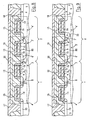
- Figure 1 shows in top-plan view and partially sectioned along several plates a portion of an array of memory cells comprising EEPROM semiconductor memory cells and ROM memory cells.
- the semiconductor memory array comprises memory cells arranged in rows (word lines) WL and columns (bit lines) BL1, BL2, ...,BL8.
- the portion of array shown in Figure 1 comprises eight ROM memory cells 2 and eight EEPROM memory cells 1 arranged symmetrically with respect to line A-A.
- each EEPROM memory cell 1 comprises a floating-gate MOSFET 3 and a selection transistor 4.
- a source region 6 and a spaced-apart drain region 7 are implanted.
- a further N-type region 8 is implanted between the drain region 7 and a part of substrate or well 5 comprised between regions 6 and 7.
- the portion of substrate or well 5 comprised between regions 6 and 7 forms a channel region, and a floating-gate electrode 9 is disposed above the channel and part of the drain region 7 with the interposition of a gate oxide layer 10 (typically of thickness comprised between 150 and 300 Angstroms), the latter having a thinner portion 11 (tunnel oxide of thickness between 70 and 120 Angstroms) at the further region 8 for allowing the passage of electrons by tunnel effect from the drain to the floating gate and vice-versa, when information is stored in the memory cell 1.
- a gate oxide layer 10 typically of thickness comprised between 150 and 300 Angstroms
- the latter having a thinner portion 11 (tunnel oxide of thickness between 70 and 120 Angstroms) at the further region 8 for allowing the passage of electrons by tunnel effect from the drain to the floating gate and vice-versa, when information is stored in the memory cell 1.
- a control gate electrode 12 is insulatively disposed above the floating-gate electrode 9.
- a selection transistor 4 is connected having an N-type source region coincident with the drain region 7 of MOSFET 3, and an N-type drain region 13 formed in the P-type substrate or well 5.
- the region of the substrate or well 5 comprised between the drain region 13 and the source region 7 of transistor 4 forms a channel region, over which two polysilicon electrodes 14, 15 are disposed, one over the other with the interposition of different layers of oxide, for forming the gate of transistor 4.
- the two polysilicon electrodes 14, 15 belong to respective lines formed from a first and a second levels of polysilicon, and said lines are electrically short-circuited in a region of the array not shown in Figure 1.
- the floating-gate electrode 9 of MOSFETs 3 of the cells 1 is formed by definition of the first level of polysilicon, while the control gate electrode 12 of MOSFET 3 of the cells 1 is formed by a respective line formed from the second level of polysilicon, such a line forming a word line WL.
- Each ROM memory cell 2 comprises, as the EEPROM cells 1, a floating-gate MOSFET 3' and, in series thereto, a selection transistor 4'.
- the ROM memory cells 2 and the EEPROM memory cells 1 are in fact formed by means of the same process steps and have identical structure.
- N-type region 80 is implanted between the drain region 7' and the source region 6' of the floating-gate MOSFET 3', with the function of short-circuiting regions 6' and 7'.
- region 80 is formed by means of the same implant used to form region 8 for the EEPROM memory cells 1.
- Lines 19 form the bit lines BL1, BL2, ...,BL8.
- reading of the EEPROM cell 1 is performed bringing the respective word line WL to a voltage of e.g. 5 V, and turning the respective selection transistor 3 on.
- the respective word line WL can be brought to 5 V or also kept at ground (it is not necessary to form the channel in the MOSFET 3', because region 80 is provided), and the respective selection transistor 4' is selected; if the contact between the respective bit line BL1, BL2, ...,BL8 and drain 13' of the selection transistor is provided, then the ROM cell 2 sink current from the bit line; if differently the contact is not provided, then the drain of the selection transistor 4' is disconnected from the bit line and no current will flow in the latter.
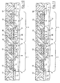
- FIG. 4-6 Another embodiment of the present invention is shown in Figures 4-6.
- apertures 17 and 18 in the dielectric layer 16 are always provided.
- Programming of the ROM cell 2 is obtained by providing or not providing the N-type region 80 which short-circuits the source 6' and the drain 7' of MOSFET 3' of the ROM cell 2.
- region 80 when region 80 is provided, the source and drain regions 6' and 7' of MOSFET 3' are short-.circuited, so that when transistor 4' is activated a current will flow through the bit line. In this case the ROM memory cell 2 stores a "1". If differently region 80 is not provided, as shown in Figure 6, when the ROM cell 2 is read turning the selection transistor 4' on and keeping the respective word line at ground (or generally at a voltage lower than the threshold voltage of MOSFET 3'), no channel will form in MOSFET 3' so that no current flows in the ROM cell, and the latter is read as a "0".
- An advantage of this embodiment with respect to the previous one is due to the impossibility of determining the code stored in the ROM cells 2 by way of a simple visual inspection of the memory array, because all the contacts to the ROM cell are present.
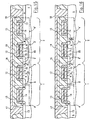
- FIG. 7-9 Another embodiment of the present invention is shown in Figures 7-9.
- both the contact with a respective bit line, through a respective opening 18 in the dielectric layer 16, and the short-circuit between source 6' and drain 7' through a respective region 80 are always provided for each ROM cell 2.
- the latter When it is desired to store a state "0" in a ROM cell 2, the latter is formed such that in the drain region 7' of the respective floating-gate MOSFET 3' (drain region which is normally formed by means of an LDD, Light Doped Drain implant) a lightly doped P-type is formed by implanting a P-type dopant with a concentration sufficient to compensate the N-type LDD implant used for forming the drain region 7' of the floating-gate MOSFET 3'.
- a lightly doped P-type is formed by implanting a P-type dopant with a concentration sufficient to compensate the N-type LDD implant used for forming the drain region 7' of the floating-gate MOSFET 3'.
- the P- region 20 forms an electrical separation region between the MOSFET 3' and the selection transistor 4' of the ROM cell 2. During reading of the ROM cell 2, no current will flow and the ROM cell 2 is thus non-conductive, independently of the voltage of the respective word line.
- the same function of the P- region 20 which separates MOSFET 3' from the selection transistor 4' can be achieved selectively preventing (where it is desired to program a "0" state) the N-type LDD implant provided for forming the drain region 7' of MOSFET 3'.
- region 20 is substituted by a portion of the substrate or well 5, and MOSFET 3' is electrically separated from the selection transistor 4' because the drain of the former is not linked to the channel of the latter (the selection transistor 4' not having the source diffusion).
- FIG. 12-14 Another embodiment of the present invention is shown in Figures 12-14.
- both the contact with a respective bit line, through a respective opening 18 in the dielectric layer 16, and the short-circuit between source 6' and drain 7' through a respective region 80 are always provided for each ROM cell 2.
- Memorization of the "0" state in a ROM cell 2 is achieved by means of an implant of a P-type dopant for forming a P- region 21 located in a portion of the drain 13 of the selection transistor 4'.
- region 21 forms an electrical separation region between the selection transistor 4' and the bit line of the ROM cell 2, so that during reading of the ROM cell 2 no current will flow in the latter, the ROM cell 2 being thus non-conductive.
- the separation region 21 can be substituted by a portion of the substrate or well 5, selectively preventing the implant used for forming the drain region 13' of the selection transistor 4', at least to the opening 18.
- the separation regions 20 and 21 can also be provided simultaneously in the same ROM cell; the result is always the programming of a "0" state. The same holds true for the absence of the N-type LDD implants that form the drain and source of the selection transistor 4'.
- FIGS 17 and 18 show an alternative of the first embodiment previously described, referring to an array of Flash-EEPROM memory cells 100 with ROM memory cells 200 having the same structure as the Flash-EEPROM cells 100.
- Each Flash-EEPROM cell 100 comprises a floating-gate MOSFET, wherein in a P-type substrate or well 5 spaced-apart N-type source and drain regions 60, 70 are implanted. The portion of substrate or well 5 comprised between regions 60 and 70 forms a channel region, and a floating-gate electrode 90 is disposed above the channel region, with the interposition of a gate oxide layer 110.
- a control gate electrode 120 is insulatively disposed over the floating-gate electrode 90.
- Each ROM memory cell 200 comprises, just as the Flash-EEPROM cells 100, a floating-gate MOSFET comprising a source region 61 separated from a drain region 71 by a channel region, and a floating-gate electrode 91 disposed over the channel region with the interposition of a gate oxide layer 111.
- a control gate electrode 121 is insulatively disposed above the floating-gate electrode 91.
- a dielectric layer 160 is successively formed, wherein openings 170 in correspondence of the drains 70 of the Flash-EEPROM cells 100 are formed.
- the gate oxide 111 of the ROM cell 200 thicker that that of the gate oxide 11o of the memory cell 100.
- the gate oxide 11I of the ROM cell 200 can be made 200 Angstroms thick, while the gate oxide 110 of the Flash-EEPROM cell 100 approximately 100 Angstroms thick.
- Another possibility is to control the voltages applied to the ROM cell during erasure of the Flash-EEPROM cells; in this case it is not necessary to form gate oxides with different thickness for the Flash-EEPROM cells and the ROM cells.
- one technique for electrically erasing the flash-EEPROM cells 100 provides for bringing the voltage of source electrodes 60 to approximately 12V, while keeping the control gates (word lines) at ground; another technique provides for biasing the source electrodes at approximately 4V and bringing the control gates to approximately -8V.
- the control gates (word lines) of the ROM cells are kept at a voltage lower than 12V, or alternatively that the control gates are kept at ground, so that the electric field in the gate oxide is sufficiently low not to trigger the tunnel effect.
- a third possibility provides for electrically short-circuiting the two polysilicon electrodes 91, 121 formed by lines in the first and second polysilicon levels, for example in a region external to the array of memory cells.
Landscapes
- Read Only Memory (AREA)
- Semiconductor Memories (AREA)
- Non-Volatile Memory (AREA)
Claims (15)
- Matrix von elektrisch programmierbaren nicht-flüchtigen Speicherzellen, wobei jede Zelle ein schwebendes Gate (9; 90), ein an eine Zeile (WL) der Matrix gekoppeltes Steuergate (12; 120), eine mit einer Spalte (BL1-B18) der Matrix verknüpfte erste Elektrode (7', 13', 71) und eine zweite Elektrode (6; 70) umfasst, die von der ersten Elektrode durch einen Kanalbereich getrennt ist, der unter dem schwebenden Gate, der ersten Elektrode, der zweiten Elektrode liegt und wobei der Kanalbereich in einer Schicht aus Halbleitermaterial (5) eines ersten Leitfähigkeitstyps ausgebildet ist und einen zweiten Leitfähigkeitstyp besitzt, zumindest eine ROM-Speicherzelle (2; 200) umfassend, die einen identischen Aufbau wie der der elektrisch programmierbaren nicht-flüchtigen Speicherzellen besitzt, und
dadurch gekennzeichnet, dass die ROM-Speicherzelle mit einer jeweiligen Zeile und einer jeweiligen Spalte der Matrix verknüpft ist, dass die ROM-Zelle (2; 200) ein Mittel (80, 18, 20, 180) umfasst, das derart ausgebildet ist, dass es die jeweilige Spalte von einer zweiten Elektrode (6'; 61) der ROM-Zelle (2; 200) elektrisch trennt, wenn die ROM-Zelle einen ersten logischen Zustand speichert, und dass das Mittel (80, 18, 20, 180) derart ausgebildet ist, dass es die jeweilige Spalte mit der zweiten Elektrode (6'; 61) der ROM-Zelle (2; 200) elektrisch verbindet, wenn die ROM-Zelle einen zweiten logischen Zustand speichert. - Matrix nach Anspruch 1, dadurch gekennzeichnet, dass das Mittel einen dotierten Halbleiterbereich (80) des zweiten Leitfähigkeitstyps umfasst, der in dem Kanalbereich der ROM-Zelle (2) ausgebildet ist zum Kurzschließen der ersten Elektrode (7'; 13') und der zweiten Elektrode (6') der ROM-Zelle (2).
- Matrix nach Anspruch 2, dadurch gekennzeichnet, dass das Mittel (80, 18) derart ausgebildet ist, dass es die jeweilige Spalte von dem Halbleiterbereich (80) elektrisch trennt in Abwesenheit eines Kontakts (18) zwischen der jeweiligen Spalte und der ersten Elektrode (7', 13') der ROM-Zelle (2), wobei das Mittel (80, 18) derart ausgebildet ist, dass es die jeweilige Spalte mit dem Halbleiterbereich (80) elektrisch verbindet in der Gegenwart eines Kontakts (18) zwischen der jeweiligen Spalte und der ersten Elektrode (7', 13') der ROM-Zelle (2).
- Matrix nach Anspruch 2, dadurch gekennzeichnet, dass das Mittel einen Kontakt (18) zwischen dem jeweiligen Schalter und der ersten Elektrode (7', 13') der ROM-Zelle (2) umfasst, wobei das Mittel (80, 18) derart ausgebildet ist, dass es die jeweilige Spalte elektrisch von dem Halbleiterbereich (80) trennt in Gegenwart eines dotierten zweiten Halbleiterbereichs (20; 21) vom ersten Leitfähigkeitstyp, der zwischen dem Kontakt (18) und dem Halbleiterbereich (80) eingefügt ist.
- Matrix nach Anspruch 4, dadurch gekennzeichnet, dass der zweite Halbleiterbereich ein Abschnitt der Halbleitermaterialschicht (5) ist.
- Matrix nach Anspruch 1, dadurch gekennzeichnet, dass das Mittel (80, 18) einen Kontakt (18) zwischen der jeweiligen Spalte und der ersten Elektrode (7', 13) der ROM-Zelle (2) umfasst, das Mittel (80, 18) derart ausgebildet ist, dass es die jeweilige Spalte von der zweiten Elektrode (61) der ROM-Zelle (2; 200) elektrisch trennt in Abwesenheit eines dotierten Halbleiterbereichs (80) des zweiten Leitfähigkeitstyps, der in dem Kanalbereich der ROM-Zelle (2) ausgebildet ist zum Kurzschließen der ersten Elektrode (7'; 13') und der zweiten Elektrode (6') der ROM-Zelle (2), wobei das Mittel (18, 80) derart ausgebildet ist, dass es die jeweilige Spalte mit der zweiten Elektrode (7', 13) der ROM-Zelle (200) elektrisch verbindet in Anwesenheit des dotierten Halbleiterbereichs (80) des zweiten Leitfähigkeitstyps, der in dem Kanalbereich der ROM-Zelle (2) ausgebildet ist zum Kurzschließen der ersten Elektrode (7'; 13') und der zweiten Elektrode (6') der ROM-Zelle (2).
- Matrix nach Anspruch 1, dadurch gekennzeichnet, dass das Mittel (180) derart ausgebildet ist, dass es die jeweilige Spalte von der zweiten Elektrode (61) der ROM-Zelle (200) elektrisch trennt in Abwesenheit eines Kontakts (180) zwischen der jeweiligen Spalte und der ersten Elektrode (71) der ROM-Zelle (2), wobei das Mittel (180) derart ausgebildet ist, dass es die jeweilige Spalte mit der zweiten Elektrode (61) der ROM-Zelle (200) elektrisch verbindet in Anwesenheit eines Kontakts (180) zwischen der jeweiligen Spalte und der ersten Elektrode (71) der ROM-Zelle (2).
- Matrix nach einem der Ansprüche 1 bis 6, dadurch gekennzeichnet, dass die elektrisch programmierbaren nicht-flüchtigen Speicherzellen EEPROM-Speicherzellen sind, die alle einen MOS-Transistor (3) mit einem schwebenden Gate, der eine durch die zweite Elektrode (6) gebildete Source-Elektrode besitzt, und einen Auswahltransistor (4) umfasst, der eine mit einer Drainelektrode (7, 8) des MOS-Transistors (3) mit schwebendem Gate verbundene Source-Elektrode (7), eine mit einer Spalte (BL1-BL8) der Matrix verbundene Drain-Elektrode (13) besitzt.
- Matrix nach Anspruch 8, wie er von Anspruch 4 abhängt, dadurch gekennzeichnet, dass der dotierte zweite Halbleiterbereich (20) des ersten Leitfähigkeitstyps an einem Sourcebereich (7') eines Auswahl-Transistors (4') der ROM-Zelle (2) ausgebildet ist.
- Matrix nach Anspruch 9, wie er von Anspruch 4 abhängt, dadurch gekennzeichnet, dass der dotierte zweite Halbleiterbereich (21) des ersten Leitfähigkeitstyps an einem Drainbereich (13') eines Auswahl-Transistors (4') der ROM-Zelle (2) ausgebildet ist.
- Matrix nach Anspruch 1 oder 7, dadurch gekennzeichnet, dass die elektrisch programmierbaren nicht-flüchtigen Speicherzellen EEPROM-Zellen sind, die alle jeweils durch einen MOS-Transistor mit schwebendem Gate gebildet sind, der eine durch die erste Elektrode gebildete Drainelektrode und eine durch die zweite Elektrode gebildete Source-Elektrode besitzt.
- Matrix nach Anspruch 1 oder 7, dadurch gekennzeichnet, dass die elektrisch programmierbaren nicht-flüchtigen Speicherzellen Flash-EEPROM-Speicherzellen (100) sind, die alle jeweils von einem MOS-Transistor mit schwebendem Gate gebildet sind, der eine durch die erste Elektrode gebildete Drain-Elektrode (70) und eine durch die zweite Elektrode gebildete Source-Elektrode (60) besitzt.
- Matrix nach Anspruch 12, dadurch gekennzeichnet, dass die ROM-Speicherzellen (200) ein Gateoxid (111) besitzen, das dicker ist als ein Gateoxid (110) der Flash-EEPROM-Speicherzellen (100).
- Matrix nach Anspruch 12, dadurch gekennzeichnet, dass die ROM-Speicherzellen (200) während des Löschvorgangs der Flash-EEPROM-Speicherzellen (100) derart ausgebildet sind, dass sie auf eine Weise vorgespannt sind, in der das elektrische Feld in dem Gateoxid ausreichend gering ist, nicht den Tunneleffekt auszulösen.
- Matrix nach Anspruch 12, dadurch gekennzeichnet, dass die ROM-Speicherzellen (200) eine schwebende Gate-Elektrode (91) und eine Steuerelektrode (121) umfassen, die zu jeweiligen Leitungen zugehörig sind, welche durch ein erstes und ein zweites Niveau aus Polysilizium gebildet sind, wobei die Elektroden in einem Bereich außerhalb der Matrix kurzgeschlossen sind.
Priority Applications (4)
| Application Number | Priority Date | Filing Date | Title |
|---|---|---|---|
| DE69734509T DE69734509D1 (de) | 1997-07-08 | 1997-07-08 | Elektrisch programmierbare, nichtflüchtige Halbleiterspeicherzellenmatrix mit ROM-Speicherzellen |
| EP97830342A EP0890985B1 (de) | 1997-07-08 | 1997-07-08 | Elektrisch programmierbare, nichtflüchtige Halbleiterspeicherzellenmatrix mit ROM-Speicherzellen |
| US09/109,487 US6259132B1 (en) | 1997-07-08 | 1998-07-02 | Array of electrically programmable non-volatile semiconductor memory cells comprising ROM memory cells |
| JP18861598A JPH1197653A (ja) | 1997-07-08 | 1998-07-03 | 電気的に書込可能な不揮発性メモリセルアレイ |
Applications Claiming Priority (1)
| Application Number | Priority Date | Filing Date | Title |
|---|---|---|---|
| EP97830342A EP0890985B1 (de) | 1997-07-08 | 1997-07-08 | Elektrisch programmierbare, nichtflüchtige Halbleiterspeicherzellenmatrix mit ROM-Speicherzellen |
Publications (2)
| Publication Number | Publication Date |
|---|---|
| EP0890985A1 EP0890985A1 (de) | 1999-01-13 |
| EP0890985B1 true EP0890985B1 (de) | 2005-11-02 |
Family
ID=8230698
Family Applications (1)
| Application Number | Title | Priority Date | Filing Date |
|---|---|---|---|
| EP97830342A Expired - Lifetime EP0890985B1 (de) | 1997-07-08 | 1997-07-08 | Elektrisch programmierbare, nichtflüchtige Halbleiterspeicherzellenmatrix mit ROM-Speicherzellen |
Country Status (4)
| Country | Link |
|---|---|
| US (1) | US6259132B1 (de) |
| EP (1) | EP0890985B1 (de) |
| JP (1) | JPH1197653A (de) |
| DE (1) | DE69734509D1 (de) |
Families Citing this family (23)
| Publication number | Priority date | Publication date | Assignee | Title |
|---|---|---|---|---|
| US5673218A (en) | 1996-03-05 | 1997-09-30 | Shepard; Daniel R. | Dual-addressed rectifier storage device |
| DE69833247D1 (de) | 1998-10-02 | 2006-04-06 | St Microelectronics Srl | Verfahren zur Herstellung eines Mehrpegel ROM Speichers in einem Doppelgate CMOS Prozess und entsprechende ROM Speicherzelle |
| US6487106B1 (en) * | 1999-01-12 | 2002-11-26 | Arizona Board Of Regents | Programmable microelectronic devices and method of forming and programming same |
| EP1024527A3 (de) * | 1998-12-31 | 2001-05-23 | STMicroelectronics S.r.l. | Verfahren zur Herstellung eines mehrwertigen Festwertspeichers (ROM) durch ein Verfahren zur Herstellung eines EEPROM-Speichers |
| US6576517B1 (en) | 1998-12-31 | 2003-06-10 | Stmicroelectronics S.R.L. | Method for obtaining a multi-level ROM in an EEPROM process flow |
| US6956757B2 (en) * | 2000-06-22 | 2005-10-18 | Contour Semiconductor, Inc. | Low cost high density rectifier matrix memory |
| US6711043B2 (en) | 2000-08-14 | 2004-03-23 | Matrix Semiconductor, Inc. | Three-dimensional memory cache system |
| US6765813B2 (en) | 2000-08-14 | 2004-07-20 | Matrix Semiconductor, Inc. | Integrated systems using vertically-stacked three-dimensional memory cells |
| FR2826169A1 (fr) * | 2001-06-15 | 2002-12-20 | St Microelectronics Sa | Memoire mos a lecture seulement |
| US6906376B1 (en) * | 2002-06-13 | 2005-06-14 | A Plus Flash Technology, Inc. | EEPROM cell structure and array architecture |
| US6768661B2 (en) | 2002-06-27 | 2004-07-27 | Matrix Semiconductor, Inc. | Multiple-mode memory and method for forming same |
| JP3941943B2 (ja) * | 2003-03-12 | 2007-07-11 | 力旺電子股▲ふん▼有限公司 | Rom |
| ATE541316T1 (de) * | 2004-11-15 | 2012-01-15 | Nxp Bv | Flash- und rom-speicher |
| KR100725171B1 (ko) * | 2006-01-06 | 2007-06-04 | 삼성전자주식회사 | 마스크 롬을 구비하는 반도체 장치 및 그 제조 방법 |
| US7813157B2 (en) * | 2007-10-29 | 2010-10-12 | Contour Semiconductor, Inc. | Non-linear conductor memory |
| US20090225621A1 (en) * | 2008-03-05 | 2009-09-10 | Shepard Daniel R | Split decoder storage array and methods of forming the same |
| FR2931289A1 (fr) * | 2008-05-13 | 2009-11-20 | St Microelectronics Rousset | Memoire a structure du type eeprom et a lecture seule |
| WO2009149061A2 (en) * | 2008-06-02 | 2009-12-10 | Contour Semiconductor, Inc. | Diode decoder array with non-sequential layout and methods of forming the same |
| US8325556B2 (en) * | 2008-10-07 | 2012-12-04 | Contour Semiconductor, Inc. | Sequencing decoder circuit |
| JP5483400B2 (ja) * | 2009-03-26 | 2014-05-07 | シチズンホールディングス株式会社 | 不揮発性半導体記憶装置 |
| CN105990367B (zh) * | 2015-02-27 | 2019-03-12 | 硅存储技术公司 | 具有rom单元的非易失性存储器单元阵列 |
| WO2016137720A1 (en) * | 2015-02-27 | 2016-09-01 | Silicon Storage Technology, Inc. | Array of non-volatile memory cells with rom cells |
| CN106158027B (zh) | 2015-04-09 | 2020-02-07 | 硅存储技术公司 | 用于对分离栅式非易失性存储器单元编程的系统和方法 |
Family Cites Families (11)
| Publication number | Priority date | Publication date | Assignee | Title |
|---|---|---|---|---|
| JPH07120720B2 (ja) * | 1987-12-17 | 1995-12-20 | 三菱電機株式会社 | 不揮発性半導体記憶装置 |
| US5122985A (en) * | 1990-04-16 | 1992-06-16 | Giovani Santin | Circuit and method for erasing eeprom memory arrays to prevent over-erased cells |
| US5488006A (en) * | 1990-09-20 | 1996-01-30 | Mitsubishi Denki Kabushiki Kaisha | One-chip microcomputer manufacturing method |
| US5227326A (en) * | 1991-12-23 | 1993-07-13 | Texas Instruments Incorporated | Method for fabricating non-volatile memory cells, arrays of non-volatile memory cells |
| JPH0729999A (ja) * | 1993-07-15 | 1995-01-31 | Mitsubishi Electric Corp | 不揮発性半導体記憶装置およびその製造方法 |
| JP3238576B2 (ja) * | 1994-08-19 | 2001-12-17 | 株式会社東芝 | 不揮発性半導体記憶装置 |
| US5894146A (en) * | 1995-02-28 | 1999-04-13 | Sgs-Thomson Microelectronics, S.R.L. | EEPROM memory cells matrix with double polysilicon level and relating manufacturing process |
| US5990512A (en) * | 1995-03-07 | 1999-11-23 | California Institute Of Technology | Hole impact ionization mechanism of hot electron injection and four-terminal ρFET semiconductor structure for long-term learning |
| EP0751559B1 (de) * | 1995-06-30 | 2002-11-27 | STMicroelectronics S.r.l. | Herstellungsverfahren eines Schaltkreises, der nichtflüchtige Speicherzellen und Randtransistoren enthält, und entsprechender IC |
| FR2738089B1 (fr) * | 1995-08-24 | 1997-10-31 | Sgs Thomson Microelectronics | Dispositif de correction de linearite de rampes d'un signal en dents de scie et generateur d'un tel signal |
| US5631486A (en) * | 1995-09-22 | 1997-05-20 | United Microelectronics Corporation | Read-only-memory having both bipolar and channel transistors |
-
1997
- 1997-07-08 DE DE69734509T patent/DE69734509D1/de not_active Expired - Lifetime
- 1997-07-08 EP EP97830342A patent/EP0890985B1/de not_active Expired - Lifetime
-
1998
- 1998-07-02 US US09/109,487 patent/US6259132B1/en not_active Expired - Lifetime
- 1998-07-03 JP JP18861598A patent/JPH1197653A/ja active Pending
Also Published As
| Publication number | Publication date |
|---|---|
| US6259132B1 (en) | 2001-07-10 |
| EP0890985A1 (de) | 1999-01-13 |
| DE69734509D1 (de) | 2005-12-08 |
| JPH1197653A (ja) | 1999-04-09 |
Similar Documents
| Publication | Publication Date | Title |
|---|---|---|
| US6259132B1 (en) | Array of electrically programmable non-volatile semiconductor memory cells comprising ROM memory cells | |
| US5787036A (en) | Flash memory including improved transistor cells and a method of programming the memory | |
| US5512504A (en) | Method of making a memory array with field oxide islands eliminated | |
| KR0159457B1 (ko) | 반도체 메모리장치 | |
| EP0639860B1 (de) | Nichtflüchtiger Halbleiterspeicher | |
| US6191975B1 (en) | Non-volatile NAND type semiconductor memory device with stacked gate memory cells and a stacked gate select transistor | |
| EP0247875B1 (de) | Blockmässig elektrisch löschbarer Speicher | |
| US7116582B2 (en) | Nonvolatile semiconductor memory and method of operating the same | |
| EP0782748B1 (de) | Nichtflüchtige speicherzellen, die nur positive ladungsträger zum speichern der daten gebrauchen | |
| JP2710521B2 (ja) | 反転層を含む半導体メモリ・セルおよびメモリ・アレイ | |
| EP1020925B1 (de) | Halbleiterspeicheranordnung und Verfahren zur Steuerung | |
| US20020164855A1 (en) | Method for forming nitride read only memory | |
| US6246088B1 (en) | Nonvolatile memory circuit and structure | |
| EP0042964A1 (de) | Speichermatrix mit Ein-Transistor-MOS-Zellen mit schwebendem Gate | |
| WO1995024057A2 (en) | Low voltage one transistor flash eeprom cell using fowler-nordheim programming and erase | |
| KR20060054966A (ko) | 플래시 메모리 장치의 동작 방법 | |
| KR100379553B1 (ko) | 플래쉬 메모리 셀의 어레이 및 이를 이용한 데이터프로그램방법 및 소거방법 | |
| JP4504518B2 (ja) | フイールドプログラム可能ゲートアレイの不揮発性メモリセルを消去する方法 | |
| EP0642172B1 (de) | Halbleiteranordnung mit einem nichtflüchtigen Speicher und Herstellungsmethode | |
| US7088623B2 (en) | Non-volatile memory technology suitable for flash and byte operation application | |
| KR101024079B1 (ko) | 실리콘 질화물 전하 포획 메모리 장치 | |
| US6963508B1 (en) | Operation method for non-volatile memory | |
| US6272046B1 (en) | Individual source line to decrease column leakage | |
| USRE37199E1 (en) | Method of making nonvolatile semiconductor memory | |
| US7139193B2 (en) | Non-volatile memory with two adjacent memory cells sharing same word line |
Legal Events
| Date | Code | Title | Description |
|---|---|---|---|
| PUAI | Public reference made under article 153(3) epc to a published international application that has entered the european phase |
Free format text: ORIGINAL CODE: 0009012 |
|
| AK | Designated contracting states |
Kind code of ref document: A1 Designated state(s): DE FR GB IT |
|
| 17P | Request for examination filed |
Effective date: 19990426 |
|
| AKX | Designation fees paid |
Free format text: DE FR GB IT |
|
| 17Q | First examination report despatched |
Effective date: 20040714 |
|
| GRAP | Despatch of communication of intention to grant a patent |
Free format text: ORIGINAL CODE: EPIDOSNIGR1 |
|
| GRAS | Grant fee paid |
Free format text: ORIGINAL CODE: EPIDOSNIGR3 |
|
| GRAA | (expected) grant |
Free format text: ORIGINAL CODE: 0009210 |
|
| AK | Designated contracting states |
Kind code of ref document: B1 Designated state(s): DE FR GB IT |
|
| REG | Reference to a national code |
Ref country code: GB Ref legal event code: FG4D |
|
| REF | Corresponds to: |
Ref document number: 69734509 Country of ref document: DE Date of ref document: 20051208 Kind code of ref document: P |
|
| PG25 | Lapsed in a contracting state [announced via postgrant information from national office to epo] |
Ref country code: DE Free format text: LAPSE BECAUSE OF FAILURE TO SUBMIT A TRANSLATION OF THE DESCRIPTION OR TO PAY THE FEE WITHIN THE PRESCRIBED TIME-LIMIT Effective date: 20060203 |
|
| PG25 | Lapsed in a contracting state [announced via postgrant information from national office to epo] |
Ref country code: GB Free format text: LAPSE BECAUSE OF NON-PAYMENT OF DUE FEES Effective date: 20060708 |
|
| ET | Fr: translation filed | ||
| PGFP | Annual fee paid to national office [announced via postgrant information from national office to epo] |
Ref country code: IT Payment date: 20060731 Year of fee payment: 10 |
|
| PLBE | No opposition filed within time limit |
Free format text: ORIGINAL CODE: 0009261 |
|
| STAA | Information on the status of an ep patent application or granted ep patent |
Free format text: STATUS: NO OPPOSITION FILED WITHIN TIME LIMIT |
|
| 26N | No opposition filed |
Effective date: 20060803 |
|
| GBPC | Gb: european patent ceased through non-payment of renewal fee |
Effective date: 20060708 |
|
| PGFP | Annual fee paid to national office [announced via postgrant information from national office to epo] |
Ref country code: FR Payment date: 20070730 Year of fee payment: 11 |
|
| REG | Reference to a national code |
Ref country code: FR Ref legal event code: ST Effective date: 20090331 |
|
| PG25 | Lapsed in a contracting state [announced via postgrant information from national office to epo] |
Ref country code: FR Free format text: LAPSE BECAUSE OF NON-PAYMENT OF DUE FEES Effective date: 20080731 |
|
| PG25 | Lapsed in a contracting state [announced via postgrant information from national office to epo] |
Ref country code: IT Free format text: LAPSE BECAUSE OF NON-PAYMENT OF DUE FEES Effective date: 20070708 |