EP0892434A2 - RF IC Gehäuse - Google Patents
RF IC Gehäuse Download PDFInfo
- Publication number
- EP0892434A2 EP0892434A2 EP98305388A EP98305388A EP0892434A2 EP 0892434 A2 EP0892434 A2 EP 0892434A2 EP 98305388 A EP98305388 A EP 98305388A EP 98305388 A EP98305388 A EP 98305388A EP 0892434 A2 EP0892434 A2 EP 0892434A2
- Authority
- EP
- European Patent Office
- Prior art keywords
- chip
- interconnection
- array
- ipwb
- substrate
- Prior art date
- Legal status (The legal status is an assumption and is not a legal conclusion. Google has not performed a legal analysis and makes no representation as to the accuracy of the status listed.)
- Granted
Links
Images
Classifications
-
- H—ELECTRICITY
- H10—SEMICONDUCTOR DEVICES; ELECTRIC SOLID-STATE DEVICES NOT OTHERWISE PROVIDED FOR
- H10W—GENERIC PACKAGES, INTERCONNECTIONS, CONNECTORS OR OTHER CONSTRUCTIONAL DETAILS OF DEVICES COVERED BY CLASS H10
- H10W44/00—Electrical arrangements for controlling or matching impedance
- H10W44/20—Electrical arrangements for controlling or matching impedance at high-frequency [HF] or radio frequency [RF]
-
- H—ELECTRICITY
- H10—SEMICONDUCTOR DEVICES; ELECTRIC SOLID-STATE DEVICES NOT OTHERWISE PROVIDED FOR
- H10W—GENERIC PACKAGES, INTERCONNECTIONS, CONNECTORS OR OTHER CONSTRUCTIONAL DETAILS OF DEVICES COVERED BY CLASS H10
- H10W70/00—Package substrates; Interposers; Redistribution layers [RDL]
- H10W70/60—Insulating or insulated package substrates; Interposers; Redistribution layers
- H10W70/611—Insulating or insulated package substrates; Interposers; Redistribution layers for connecting multiple chips together
-
- H—ELECTRICITY
- H10—SEMICONDUCTOR DEVICES; ELECTRIC SOLID-STATE DEVICES NOT OTHERWISE PROVIDED FOR
- H10W—GENERIC PACKAGES, INTERCONNECTIONS, CONNECTORS OR OTHER CONSTRUCTIONAL DETAILS OF DEVICES COVERED BY CLASS H10
- H10W90/00—Package configurations
-
- H—ELECTRICITY
- H10—SEMICONDUCTOR DEVICES; ELECTRIC SOLID-STATE DEVICES NOT OTHERWISE PROVIDED FOR
- H10W—GENERIC PACKAGES, INTERCONNECTIONS, CONNECTORS OR OTHER CONSTRUCTIONAL DETAILS OF DEVICES COVERED BY CLASS H10
- H10W90/00—Package configurations
- H10W90/401—Package configurations characterised by multiple insulating or insulated package substrates, interposers or RDLs
-
- H—ELECTRICITY
- H10—SEMICONDUCTOR DEVICES; ELECTRIC SOLID-STATE DEVICES NOT OTHERWISE PROVIDED FOR
- H10W—GENERIC PACKAGES, INTERCONNECTIONS, CONNECTORS OR OTHER CONSTRUCTIONAL DETAILS OF DEVICES COVERED BY CLASS H10
- H10W70/00—Package substrates; Interposers; Redistribution layers [RDL]
- H10W70/60—Insulating or insulated package substrates; Interposers; Redistribution layers
- H10W70/67—Insulating or insulated package substrates; Interposers; Redistribution layers characterised by their insulating layers or insulating parts
- H10W70/68—Shapes or dispositions thereof
- H10W70/681—Shapes or dispositions thereof comprising holes not having chips therein, e.g. for outgassing, underfilling or bond wire passage
-
- H—ELECTRICITY
- H10—SEMICONDUCTOR DEVICES; ELECTRIC SOLID-STATE DEVICES NOT OTHERWISE PROVIDED FOR
- H10W—GENERIC PACKAGES, INTERCONNECTIONS, CONNECTORS OR OTHER CONSTRUCTIONAL DETAILS OF DEVICES COVERED BY CLASS H10
- H10W72/00—Interconnections or connectors in packages
- H10W72/851—Dispositions of multiple connectors or interconnections
- H10W72/874—On different surfaces
- H10W72/877—Bump connectors and die-attach connectors
-
- H—ELECTRICITY
- H10—SEMICONDUCTOR DEVICES; ELECTRIC SOLID-STATE DEVICES NOT OTHERWISE PROVIDED FOR
- H10W—GENERIC PACKAGES, INTERCONNECTIONS, CONNECTORS OR OTHER CONSTRUCTIONAL DETAILS OF DEVICES COVERED BY CLASS H10
- H10W90/00—Package configurations
- H10W90/701—Package configurations characterised by the relative positions of pads or connectors relative to package parts
- H10W90/721—Package configurations characterised by the relative positions of pads or connectors relative to package parts of bump connectors
- H10W90/724—Package configurations characterised by the relative positions of pads or connectors relative to package parts of bump connectors between a chip and a stacked insulating package substrate, interposer or RDL
Definitions
- This invention relates to multi-chip module (MCM) integrated circuit packages and more specifically to MCM packages containing at least one RF chip.
- MCM multi-chip module
- a preferred arrangement is to flip chip bond the individual chips to a MCM tile, mount the MCM tile on an intermediate printed wiring board (IPWB) which in turn in mounted on a system board (SPWB).
- IPWB intermediate printed wiring board
- SPWB system board
- typically three interconnections are made between the chip and the system board, i.e. chip to MCM, MCM to IPWB and IPWB to SPWB.
- the ground interconnection for the RF chip is made directly between the chip and the SPWB, thus reducing the length and impedance of the conventional ground connection.
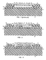
- a multi-chip tile comprising IC chips 11 and 12, and substrate 13.
- the IC 11 in this arrangement is an RF chip.
- Chip 12 is not an RF chip, e.g. a logic or memory chip. This choice is for illustration.
- the interconnection of any combination of IC chips that includes at least one RF chip, or an RF chip alone in the MCM tile, can be implemented following the teachings of the invention.
- the MCM tile may also contain passive components, e.g. capacitors, inductors, and resistors.
- a typical arrangement is an RF circuit chip and a capacitor mounted on the substrate 13.
- the substrate can be laminate, ceramic, silicon, or other appropriate material.
- the chips 11 and 12 are flip chip bonded to substrate 13 by interconnections 14 such as solder or conductive epoxy.
- interconnections 14 such as solder or conductive epoxy.
- the technique used for the flip chip bond is not part of the invention and may e.g. be solder bump, ball bonding, or conductive epoxy etc.
- the MCM tile 13 is in turn flip bonded to intermediate printed wiring board (IPWB) 15 with solder or conductive epoxy I/O interconnections 16.
- IPWB 15 is shown as an multilevel board, but may be single level.
- the IPWB is in turn interconnected to a system board (SPWB) 18 by solder or conductive epoxy interconnections 17.
- SPWB may also be single or multi-level, and is shown here with a separate level 19.
- a cutway portion of the SPWB is shown to illustrate that the system board may be considerably larger than the IPWB to accommodate several IPWBs.
- the interconnect elements 13 and 15 are quad packages with a large array of I/O bonding sites arranged in a square or rectangular configuration.
- a single interconnection for the ground connection is shown to illustrate the invention.
- the ground connection is designated 22 on the chip 11 and 12, and connects to the SPWB via the interconnect substrate runners 23, the solder interconnections 16, through the IPWB and the interconnections 17, to the common ground plane 21 of the SPWB.
- the ground connection for all chips is made in essentially the same way.
- the remaining I/O connections are not shown but are also conventional.
- the elements common to both figures have the same reference numbers.
- the change is evident in the manner in which the ground connection is made between the RF chip 11 and the common ground plane 21 of the SPWB.
- the backside of the RF chip is metallized with metallization layer 32.
- Metallizing the backside of the RF chip is made possible by the flip chip bonding arrangement.
- the metallization should be applied directly to the semiconductor and any oxide that has been grown or deposited, or native oxide formed during processing, should be removed prior to metallization. It is preferred to apply the metallization to the chip at the wafer stage, where it can be applied at any convenient point in the wafer fabrication sequence.
- the material used for the metallization can be any appropriate conductive material, e.g. Au, Cr/CrCu/Cu, TiPdAu, Al.
- a solder wettable metal or metal such as TiPdAu is preferred as it can facilitate direct soldering to the ground pad 34.
- the metallized RF chip is then bonded by conductive material 33 directly to a ground plane pad 34 on the SPWB.
- the ground plane pad 34 is part of the common ground 21 of the SPWB. It is preferable to locate the common ground plane 21 on the same level as the bond pad 34, but alternative arrangements, like those shown in these figures, are also effective.
- the bond 33 between the RF chip and the SPWB is made at the same time the IPWB is interconnected to the SPWB.
- the bonding material and the bonding technique there are various appropriate alternatives for the bonding material and the bonding technique.
- the preferred approach is to effect bonds 33 in the same way as bonds 17 using a standard surface mount approach.
- solder paste is used for interconnecting the IPWB with the SPWB, solder paste interconnection is made between RF chip 11 and SPWB 18 in the same step.
- conductive epoxy is another choice.
- Solder bumps or balls could also be used.
- the other chip 12 shown in Fig. 2 which in this example is not an RF chip, may be grounded to SPWB in the conventional way as shown here, or it may be grounded in the same manner as RF chip 11.
- Fig. 3 An embodiment alternative to that of Fig.2 is shown in Fig. 3.
- bond 33 is preferably a conductive epoxy bond.
- it is conventional to fill the gap between the chips and the SPWB with epoxy underfill, mainly for mechanical reasons, i.e. the physical integrity of the package.
- the epoxy filling material is shown at 41.
- Chip 12 is shown grounded in the same manner as chip 11.
- the epoxy filling material is applied only between the IC chips 11 and 12 and the MCM tile 13, or only between the chips, the tile and the IPWB 15.
- anisotropic conductive polymer functions both as an underfill material, and also provides an effective low impedance ground connection for the RF chip 11. In this embodiment, it is most expedient to ground all the chips in the MCM tile by the same technique.
- the invention is applicable to PWB interconnection arrangements wherein the intermediate PWB has an opening that extends completely through the thickness of the board and the MCM is mounted so as to recess significantly below the surface of the board, thus reducing the package profile.
- This PWB structure is described and claimed in U. S. Patent No. 5,608,262, issued Mar. 4, 1997.
- Such structures are quadrangular in shape, and frequently square in shape.
- the interior opening in these structures is typically congruent with the outer geometry and has, for the purpose of defining the invention, a picture frame structure.
- the dimensions, in particular the thickness, of the elements in the MCM should be such that the metallized surface of the RF chip is nearly in contact with said SPWB. Accordingly, to achieve that result, the thickness separating the interconnections between the interconnect substrate and the IPWB and the interconnections between the IPWB and the SPWB should be approximately the thickness of the RF chip, as in the MCM configuration shown in Figs. 2 and 3. In more complex MCM configurations , the RF chip may be flip chip bonded to another chip in the MCM (which configuration should be regarded as within the scope of the invention).
- the combined thickness of the chips should approximate the thickness separating the interconnections between the substrate and the IPWB and the interconnections between the IPWB and the SPWB.
- a more direct way to specify this relationship is that with the IPWB installed on the SPWB, the metallized surface of the RF chip, and the array of interconnection sites interconnecting the IPWB with the SPWB, are essentially coplanar.
- the IPWB has two arrays of interconnection sites, one array on one side of the picture frame structure, and adapted to interconnect with a corresponding array of interconnection sites on the SPWB, and a second array of interconnection sites on the other side of said IPWB adapted to be interconnected to a corresponding interconnection array on the interconnect substrate of the MCM.
- the interconnect substrate of the MCM also has two array of interconnection sites, but both arrays are on the same side of the interconnect substrate.
- One array the outer array typically around the periphery of the interconnect substrate, is adapted to interconnect with the IPWB, as just described, and the other array, an inner array, is adapted to be interconnected to a corresponding array on the RF IC chip.
- the RF chip has a circuit side where the IC is fabricated, and an underside which according to a feature of the invention is metallalized.
- the circuit side is bonded to the interconnect substrate, and the metallalized surface is exposed.
- the MCM tile is also bonded "upside down" to the IPWB so that when the IPWB is attached to the SPWB the exposed metallized surface of the RF chip is adjacent the SPWB to allow direct bonding between them.
Landscapes
- Wire Bonding (AREA)
- Structures For Mounting Electric Components On Printed Circuit Boards (AREA)
- Combinations Of Printed Boards (AREA)
Applications Claiming Priority (2)
| Application Number | Priority Date | Filing Date | Title |
|---|---|---|---|
| US896917 | 1997-07-18 | ||
| US08/896,917 US5869894A (en) | 1997-07-18 | 1997-07-18 | RF IC package |
Publications (3)
| Publication Number | Publication Date |
|---|---|
| EP0892434A2 true EP0892434A2 (de) | 1999-01-20 |
| EP0892434A3 EP0892434A3 (de) | 1999-09-01 |
| EP0892434B1 EP0892434B1 (de) | 2008-10-15 |
Family
ID=25407058
Family Applications (1)
| Application Number | Title | Priority Date | Filing Date |
|---|---|---|---|
| EP98305388A Expired - Lifetime EP0892434B1 (de) | 1997-07-18 | 1998-07-07 | RF IC Gehäuse |
Country Status (4)
| Country | Link |
|---|---|
| US (1) | US5869894A (de) |
| EP (1) | EP0892434B1 (de) |
| JP (1) | JP3215374B2 (de) |
| DE (1) | DE69840118D1 (de) |
Cited By (7)
| Publication number | Priority date | Publication date | Assignee | Title |
|---|---|---|---|---|
| US6469395B1 (en) | 1999-11-25 | 2002-10-22 | Mitsubishi Denki Kabushiki Kaisha | Semiconductor device |
| WO2003046989A3 (en) * | 2001-11-27 | 2003-10-09 | Koninkl Philips Electronics Nv | Multi-chip module semiconductor devices |
| DE10229038A1 (de) * | 2002-06-28 | 2004-01-29 | Robert Bosch Gmbh | Mikrostrukturbauelement, insbesondere mikrostrukturiertes Hochfrequenzbauelement |
| WO2003085725A3 (en) * | 2002-04-01 | 2004-09-10 | Intel Corp | In package power supplies for integrated circuits |
| EP0959500A3 (de) * | 1998-05-19 | 2004-09-29 | Lucent Technologies Inc. | Siliziumverpackung auf Silizium Multichipmodulen |
| EP1189280A4 (de) * | 2000-03-29 | 2005-03-02 | Rohm Co Ltd | Halbleiter |
| US7262680B2 (en) | 2004-02-27 | 2007-08-28 | Illinois Institute Of Technology | Compact inductor with stacked via magnetic cores for integrated circuits |
Families Citing this family (87)
| Publication number | Priority date | Publication date | Assignee | Title |
|---|---|---|---|---|
| US6018463A (en) * | 1997-08-22 | 2000-01-25 | Raytheon Company | Large non-hermetic multichip module package |
| US6154370A (en) * | 1998-07-21 | 2000-11-28 | Lucent Technologies Inc. | Recessed flip-chip package |
| US6329713B1 (en) * | 1998-10-21 | 2001-12-11 | International Business Machines Corporation | Integrated circuit chip carrier assembly comprising a stiffener attached to a dielectric substrate |
| KR100470386B1 (ko) * | 1998-12-26 | 2005-05-19 | 주식회사 하이닉스반도체 | 멀티-칩패키지 |
| US6201302B1 (en) * | 1998-12-31 | 2001-03-13 | Sampo Semiconductor Corporation | Semiconductor package having multi-dies |
| JP2000223645A (ja) * | 1999-02-01 | 2000-08-11 | Mitsubishi Electric Corp | 半導体装置 |
| US6204562B1 (en) * | 1999-02-11 | 2001-03-20 | United Microelectronics Corp. | Wafer-level chip scale package |
| JP2000252414A (ja) * | 1999-03-04 | 2000-09-14 | Mitsubishi Electric Corp | 半導体装置 |
| US6268660B1 (en) * | 1999-03-05 | 2001-07-31 | International Business Machines Corporation | Silicon packaging with through wafer interconnects |
| JP2000260912A (ja) * | 1999-03-05 | 2000-09-22 | Fujitsu Ltd | 半導体装置の実装構造及び半導体装置の実装方法 |
| US6034425A (en) * | 1999-03-17 | 2000-03-07 | Chipmos Technologies Inc. | Flat multiple-chip module micro ball grid array packaging |
| US6215193B1 (en) * | 1999-04-21 | 2001-04-10 | Advanced Semiconductor Engineering, Inc. | Multichip modules and manufacturing method therefor |
| US6127726A (en) * | 1999-05-27 | 2000-10-03 | Lsi Logic Corporation | Cavity down plastic ball grid array multi-chip module |
| US6335566B1 (en) * | 1999-06-17 | 2002-01-01 | Hitachi, Ltd. | Semiconductor device and an electronic device |
| SE514426C2 (sv) * | 1999-06-17 | 2001-02-19 | Ericsson Telefon Ab L M | Anordning för chipmontering i kavitet i flerlagers mönsterkort |
| JP2001077293A (ja) * | 1999-09-02 | 2001-03-23 | Nec Corp | 半導体装置 |
| US6297551B1 (en) * | 1999-09-22 | 2001-10-02 | Agere Systems Guardian Corp. | Integrated circuit packages with improved EMI characteristics |
| US6369448B1 (en) | 2000-01-21 | 2002-04-09 | Lsi Logic Corporation | Vertically integrated flip chip semiconductor package |
| JP3996315B2 (ja) * | 2000-02-21 | 2007-10-24 | 松下電器産業株式会社 | 半導体装置およびその製造方法 |
| US7247932B1 (en) * | 2000-05-19 | 2007-07-24 | Megica Corporation | Chip package with capacitor |
| US6569754B2 (en) * | 2000-08-24 | 2003-05-27 | The Regents Of The University Of Michigan | Method for making a module including a microplatform |
| TW569403B (en) * | 2001-04-12 | 2004-01-01 | Siliconware Precision Industries Co Ltd | Multi-chip module and its manufacturing method |
| CN1184684C (zh) * | 2000-10-05 | 2005-01-12 | 三洋电机株式会社 | 半导体装置和半导体模块 |
| JP3520039B2 (ja) * | 2000-10-05 | 2004-04-19 | 三洋電機株式会社 | 半導体装置および半導体モジュール |
| TW472372B (en) * | 2001-01-17 | 2002-01-11 | Siliconware Precision Industries Co Ltd | Memory module with direct chip attach and the manufacturing process thereof |
| JP3929250B2 (ja) * | 2001-03-08 | 2007-06-13 | 株式会社ルネサステクノロジ | 半導体装置 |
| SG108245A1 (en) * | 2001-03-30 | 2005-01-28 | Micron Technology Inc | Ball grid array interposer, packages and methods |
| US6856007B2 (en) * | 2001-08-28 | 2005-02-15 | Tessera, Inc. | High-frequency chip packages |
| US7176506B2 (en) * | 2001-08-28 | 2007-02-13 | Tessera, Inc. | High frequency chip packages with connecting elements |
| US6979894B1 (en) | 2001-09-27 | 2005-12-27 | Marvell International Ltd. | Integrated chip package having intermediate substrate |
| US6942018B2 (en) | 2001-09-28 | 2005-09-13 | The Board Of Trustees Of The Leland Stanford Junior University | Electroosmotic microchannel cooling system |
| US7134486B2 (en) * | 2001-09-28 | 2006-11-14 | The Board Of Trustees Of The Leeland Stanford Junior University | Control of electrolysis gases in electroosmotic pump systems |
| TW523887B (en) | 2001-11-15 | 2003-03-11 | Siliconware Precision Industries Co Ltd | Semiconductor packaged device and its manufacturing method |
| US6998292B2 (en) * | 2001-11-30 | 2006-02-14 | Vitesse Semiconductor Corporation | Apparatus and method for inter-chip or chip-to-substrate connection with a sub-carrier |
| US6606251B1 (en) | 2002-02-07 | 2003-08-12 | Cooligy Inc. | Power conditioning module |
| US7573136B2 (en) * | 2002-06-27 | 2009-08-11 | Micron Technology, Inc. | Semiconductor device assemblies and packages including multiple semiconductor device components |
| US6906415B2 (en) * | 2002-06-27 | 2005-06-14 | Micron Technology, Inc. | Semiconductor device assemblies and packages including multiple semiconductor devices and methods |
| US6661100B1 (en) * | 2002-07-30 | 2003-12-09 | International Business Machines Corporation | Low impedance power distribution structure for a semiconductor chip package |
| US20040068867A1 (en) * | 2002-10-15 | 2004-04-15 | Burton Edward Allyn | Land-side mounting of components to an integrated circuit package |
| TW578292B (en) * | 2002-11-22 | 2004-03-01 | Via Tech Inc | Chip to eliminate noise and manufacturing method thereof |
| US6906598B2 (en) | 2002-12-31 | 2005-06-14 | Mcnc | Three dimensional multimode and optical coupling devices |
| US7388294B2 (en) * | 2003-01-27 | 2008-06-17 | Micron Technology, Inc. | Semiconductor components having stacked dice |
| US7754537B2 (en) * | 2003-02-25 | 2010-07-13 | Tessera, Inc. | Manufacture of mountable capped chips |
| JP2004271312A (ja) * | 2003-03-07 | 2004-09-30 | Denso Corp | 容量型半導体センサ装置 |
| US6770159B1 (en) * | 2003-03-26 | 2004-08-03 | Harris Corporation | Method of fabricating an RF substrate with selected electrical properties |
| US7414505B2 (en) * | 2003-05-13 | 2008-08-19 | Samsung Electronics Co., Ltd. | High frequency inductor having low inductance and low inductance variation and method of manufacturing the same |
| US6972480B2 (en) | 2003-06-16 | 2005-12-06 | Shellcase Ltd. | Methods and apparatus for packaging integrated circuit devices |
| WO2005004195A2 (en) | 2003-07-03 | 2005-01-13 | Shellcase Ltd. | Method and apparatus for packaging integrated circuit devices |
| US6825567B1 (en) * | 2003-08-19 | 2004-11-30 | Advanced Semiconductor Engineering, Inc. | Face-to-face multi-chip flip-chip package |
| US7224056B2 (en) * | 2003-09-26 | 2007-05-29 | Tessera, Inc. | Back-face and edge interconnects for lidded package |
| US20050067681A1 (en) * | 2003-09-26 | 2005-03-31 | Tessera, Inc. | Package having integral lens and wafer-scale fabrication method therefor |
| US7181834B2 (en) * | 2003-10-27 | 2007-02-27 | Harris Corporation | Method of fabricating an RF substrate with selected electrical properties |
| US7253517B2 (en) * | 2003-10-28 | 2007-08-07 | Raytheon Company | Method and apparatus for combining multiple integrated circuits |
| US20050139984A1 (en) * | 2003-12-19 | 2005-06-30 | Tessera, Inc. | Package element and packaged chip having severable electrically conductive ties |
| US7521785B2 (en) * | 2003-12-23 | 2009-04-21 | Tessera, Inc. | Packaged systems with MRAM |
| WO2005086532A2 (en) * | 2004-03-01 | 2005-09-15 | Tessera, Inc. | Packaged acoustic and electromagnetic transducer chips |
| US8143095B2 (en) * | 2005-03-22 | 2012-03-27 | Tessera, Inc. | Sequential fabrication of vertical conductive interconnects in capped chips |
| KR100643935B1 (ko) * | 2005-06-30 | 2006-11-10 | 삼성전기주식회사 | 병렬 칩 내장 인쇄회로기판 및 그 제조방법 |
| US20070014095A1 (en) * | 2005-07-12 | 2007-01-18 | Weiss Roger E | High-performance separable electrical device/printed circuit board interconnection |
| US7936062B2 (en) * | 2006-01-23 | 2011-05-03 | Tessera Technologies Ireland Limited | Wafer level chip packaging |
| US20070190747A1 (en) * | 2006-01-23 | 2007-08-16 | Tessera Technologies Hungary Kft. | Wafer level packaging to lidded chips |
| US20080002460A1 (en) * | 2006-03-01 | 2008-01-03 | Tessera, Inc. | Structure and method of making lidded chips |
| US7638867B2 (en) * | 2006-06-02 | 2009-12-29 | Intel Corporation | Microelectronic package having solder-filled through-vias |
| US7999383B2 (en) * | 2006-07-21 | 2011-08-16 | Bae Systems Information And Electronic Systems Integration Inc. | High speed, high density, low power die interconnect system |
| JP2008166527A (ja) * | 2006-12-28 | 2008-07-17 | Spansion Llc | 半導体装置およびその製造方法 |
| US7863189B2 (en) * | 2007-01-05 | 2011-01-04 | International Business Machines Corporation | Methods for fabricating silicon carriers with conductive through-vias with low stress and low defect density |
| US8604605B2 (en) | 2007-01-05 | 2013-12-10 | Invensas Corp. | Microelectronic assembly with multi-layer support structure |
| DE102007009521B4 (de) * | 2007-02-27 | 2011-12-15 | Infineon Technologies Ag | Bauteil und Verfahren zu dessen Herstellung |
| US20080284037A1 (en) | 2007-05-15 | 2008-11-20 | Andry Paul S | Apparatus and Methods for Constructing Semiconductor Chip Packages with Silicon Space Transformer Carriers |
| US20090184416A1 (en) | 2008-01-22 | 2009-07-23 | Yinon Degani | MCM packages |
| US8259454B2 (en) * | 2008-04-14 | 2012-09-04 | General Electric Company | Interconnect structure including hybrid frame panel |
| JP2010074072A (ja) * | 2008-09-22 | 2010-04-02 | Nec Corp | 半導体装置および半導体装置の製造方法 |
| JP2012114241A (ja) * | 2010-11-25 | 2012-06-14 | Renesas Electronics Corp | 半導体チップおよび半導体装置 |
| US8737080B2 (en) * | 2011-01-14 | 2014-05-27 | Qualcomm Incorporated | Modular surface mount package for a system on a chip |
| US9693492B2 (en) | 2011-04-14 | 2017-06-27 | Mitsubishi Electric Corporation | High-frequency package |
| US8704384B2 (en) | 2012-02-17 | 2014-04-22 | Xilinx, Inc. | Stacked die assembly |
| US8704364B2 (en) * | 2012-02-08 | 2014-04-22 | Xilinx, Inc. | Reducing stress in multi-die integrated circuit structures |
| US8957512B2 (en) | 2012-06-19 | 2015-02-17 | Xilinx, Inc. | Oversized interposer |
| US8869088B1 (en) | 2012-06-27 | 2014-10-21 | Xilinx, Inc. | Oversized interposer formed from a multi-pattern region mask |
| US9026872B2 (en) | 2012-08-16 | 2015-05-05 | Xilinx, Inc. | Flexible sized die for use in multi-die integrated circuit |
| US9196575B1 (en) * | 2013-02-04 | 2015-11-24 | Altera Corporation | Integrated circuit package with cavity in substrate |
| CN103165769B (zh) * | 2013-02-28 | 2015-05-13 | 溧阳市宏达电机有限公司 | 一种发光二极管的制造方法 |
| US9547034B2 (en) | 2013-07-03 | 2017-01-17 | Xilinx, Inc. | Monolithic integrated circuit die having modular die regions stitched together |
| CN106464218B (zh) * | 2014-02-25 | 2019-05-10 | 天工方案公司 | 关于改进的射频模块的系统、设备和方法 |
| US9915869B1 (en) | 2014-07-01 | 2018-03-13 | Xilinx, Inc. | Single mask set used for interposer fabrication of multiple products |
| TWI653919B (zh) * | 2017-08-10 | 2019-03-11 | 晶巧股份有限公司 | 高散熱等線距堆疊晶片封裝結構和方法 |
| CN116601757B (zh) * | 2020-12-11 | 2025-07-22 | 株式会社村田制作所 | 高频模块和通信装置 |
Family Cites Families (6)
| Publication number | Priority date | Publication date | Assignee | Title |
|---|---|---|---|---|
| US5138436A (en) * | 1990-11-16 | 1992-08-11 | Ball Corporation | Interconnect package having means for waveguide transmission of rf signals |
| US5198963A (en) * | 1991-11-21 | 1993-03-30 | Motorola, Inc. | Multiple integrated circuit module which simplifies handling and testing |
| DE19506759C2 (de) * | 1994-02-28 | 2000-08-17 | Mitsubishi Electric Corp | Halbleitervorrichtung und Verfahren für deren Herstellung |
| TW373308B (en) * | 1995-02-24 | 1999-11-01 | Agere Systems Inc | Thin packaging of multi-chip modules with enhanced thermal/power management |
| US5608262A (en) * | 1995-02-24 | 1997-03-04 | Lucent Technologies Inc. | Packaging multi-chip modules without wire-bond interconnection |
| WO1998015979A1 (en) * | 1996-10-10 | 1998-04-16 | Samsung Electronics Co., Ltd. | Ehf and microwave-frequency multilayered hybrid and integrated circuit |
-
1997
- 1997-07-18 US US08/896,917 patent/US5869894A/en not_active Expired - Lifetime
-
1998
- 1998-07-07 EP EP98305388A patent/EP0892434B1/de not_active Expired - Lifetime
- 1998-07-07 DE DE69840118T patent/DE69840118D1/de not_active Expired - Lifetime
- 1998-07-17 JP JP20241898A patent/JP3215374B2/ja not_active Expired - Fee Related
Cited By (10)
| Publication number | Priority date | Publication date | Assignee | Title |
|---|---|---|---|---|
| EP0959500A3 (de) * | 1998-05-19 | 2004-09-29 | Lucent Technologies Inc. | Siliziumverpackung auf Silizium Multichipmodulen |
| US6469395B1 (en) | 1999-11-25 | 2002-10-22 | Mitsubishi Denki Kabushiki Kaisha | Semiconductor device |
| EP1189280A4 (de) * | 2000-03-29 | 2005-03-02 | Rohm Co Ltd | Halbleiter |
| WO2003046989A3 (en) * | 2001-11-27 | 2003-10-09 | Koninkl Philips Electronics Nv | Multi-chip module semiconductor devices |
| CN100442504C (zh) * | 2001-11-27 | 2008-12-10 | Nxp股份有限公司 | 多芯片模块半导体器件 |
| WO2003085725A3 (en) * | 2002-04-01 | 2004-09-10 | Intel Corp | In package power supplies for integrated circuits |
| US7823279B2 (en) | 2002-04-01 | 2010-11-02 | Intel Corporation | Method for using an in package power supply to supply power to an integrated circuit and to a component |
| DE10229038A1 (de) * | 2002-06-28 | 2004-01-29 | Robert Bosch Gmbh | Mikrostrukturbauelement, insbesondere mikrostrukturiertes Hochfrequenzbauelement |
| DE10229038B4 (de) * | 2002-06-28 | 2013-08-14 | Robert Bosch Gmbh | Verkapptes Mikrostrukturbauelement mit Hochfrequenzdurchführung |
| US7262680B2 (en) | 2004-02-27 | 2007-08-28 | Illinois Institute Of Technology | Compact inductor with stacked via magnetic cores for integrated circuits |
Also Published As
| Publication number | Publication date |
|---|---|
| EP0892434A3 (de) | 1999-09-01 |
| DE69840118D1 (de) | 2008-11-27 |
| EP0892434B1 (de) | 2008-10-15 |
| JPH1187549A (ja) | 1999-03-30 |
| JP3215374B2 (ja) | 2001-10-02 |
| US5869894A (en) | 1999-02-09 |
Similar Documents
| Publication | Publication Date | Title |
|---|---|---|
| US5869894A (en) | RF IC package | |
| US6154370A (en) | Recessed flip-chip package | |
| US8236608B2 (en) | Stacking package structure with chip embedded inside and die having through silicon via and method of the same | |
| US5311059A (en) | Backplane grounding for flip-chip integrated circuit | |
| US20020074637A1 (en) | Stacked flip chip assemblies | |
| US6437990B1 (en) | Multi-chip ball grid array IC packages | |
| US8129221B2 (en) | Semiconductor package and method of forming the same | |
| US6734539B2 (en) | Stacked module package | |
| JP6789219B2 (ja) | 画像センサデバイス | |
| US6558978B1 (en) | Chip-over-chip integrated circuit package | |
| US6833628B2 (en) | Mutli-chip module | |
| US6274930B1 (en) | Multi-chip module with stacked dice | |
| US6344401B1 (en) | Method of forming a stacked-die integrated circuit chip package on a water level | |
| KR100269528B1 (ko) | 고성능 멀티 칩 모듈 패키지 | |
| US20090166873A1 (en) | Inter-connecting structure for semiconductor device package and method of the same | |
| KR20020055603A (ko) | 이중 다이 집적 회로 패키지 | |
| US20090057867A1 (en) | Integrated Circuit Package with Passive Component | |
| US20090008777A1 (en) | Inter-connecting structure for semiconductor device package and method of the same | |
| US6107121A (en) | Method of making interconnections between a multi-layer chip stack to a printed circuit board in a ceramic package | |
| US6558981B2 (en) | Method for making an encapsulated semiconductor chip module | |
| EP0908951A3 (de) | Verbesserte luftisolierte Kreuzungsstruktur | |
| US20230378072A1 (en) | Electronic package and manufacturing method thereof | |
| WO1998048449A2 (en) | Flip chip and chip scale package | |
| JPH05259374A (ja) | 高密度実装配線基板およびその高密度実装方法 | |
| WO2002003465A2 (en) | Semiconductor package with stacked flip chip and wire bonded upper die |
Legal Events
| Date | Code | Title | Description |
|---|---|---|---|
| PUAI | Public reference made under article 153(3) epc to a published international application that has entered the european phase |
Free format text: ORIGINAL CODE: 0009012 |
|
| AK | Designated contracting states |
Kind code of ref document: A2 Designated state(s): DE FR GB |
|
| AX | Request for extension of the european patent |
Free format text: AL;LT;LV;MK;RO;SI |
|
| PUAL | Search report despatched |
Free format text: ORIGINAL CODE: 0009013 |
|
| AK | Designated contracting states |
Kind code of ref document: A3 Designated state(s): AT BE CH CY DE DK ES FI FR GB GR IE IT LI LU MC NL PT SE |
|
| AX | Request for extension of the european patent |
Free format text: AL;LT;LV;MK;RO;SI |
|
| 17P | Request for examination filed |
Effective date: 20000218 |
|
| AKX | Designation fees paid |
Free format text: DE FR GB |
|
| GRAP | Despatch of communication of intention to grant a patent |
Free format text: ORIGINAL CODE: EPIDOSNIGR1 |
|
| GRAS | Grant fee paid |
Free format text: ORIGINAL CODE: EPIDOSNIGR3 |
|
| GRAA | (expected) grant |
Free format text: ORIGINAL CODE: 0009210 |
|
| AK | Designated contracting states |
Kind code of ref document: B1 Designated state(s): DE FR GB |
|
| REG | Reference to a national code |
Ref country code: GB Ref legal event code: FG4D |
|
| REF | Corresponds to: |
Ref document number: 69840118 Country of ref document: DE Date of ref document: 20081127 Kind code of ref document: P |
|
| PLBE | No opposition filed within time limit |
Free format text: ORIGINAL CODE: 0009261 |
|
| STAA | Information on the status of an ep patent application or granted ep patent |
Free format text: STATUS: NO OPPOSITION FILED WITHIN TIME LIMIT |
|
| RAP4 | Party data changed (patent owner data changed or rights of a patent transferred) |
Owner name: LUCENT TECHNOLOGIES INC. |
|
| 26N | No opposition filed |
Effective date: 20090716 |
|
| PGFP | Annual fee paid to national office [announced via postgrant information from national office to epo] |
Ref country code: FR Payment date: 20140708 Year of fee payment: 17 |
|
| REG | Reference to a national code |
Ref country code: DE Ref legal event code: R082 Ref document number: 69840118 Country of ref document: DE Representative=s name: DILG HAEUSLER SCHINDELMANN PATENTANWALTSGESELL, DE |
|
| PGFP | Annual fee paid to national office [announced via postgrant information from national office to epo] |
Ref country code: GB Payment date: 20150626 Year of fee payment: 18 |
|
| REG | Reference to a national code |
Ref country code: FR Ref legal event code: ST Effective date: 20160331 |
|
| PG25 | Lapsed in a contracting state [announced via postgrant information from national office to epo] |
Ref country code: FR Free format text: LAPSE BECAUSE OF NON-PAYMENT OF DUE FEES Effective date: 20150731 |
|
| GBPC | Gb: european patent ceased through non-payment of renewal fee |
Effective date: 20160707 |
|
| PG25 | Lapsed in a contracting state [announced via postgrant information from national office to epo] |
Ref country code: GB Free format text: LAPSE BECAUSE OF NON-PAYMENT OF DUE FEES Effective date: 20160707 |
|
| PGFP | Annual fee paid to national office [announced via postgrant information from national office to epo] |
Ref country code: DE Payment date: 20170620 Year of fee payment: 20 |
|
| REG | Reference to a national code |
Ref country code: DE Ref legal event code: R071 Ref document number: 69840118 Country of ref document: DE |
|
| REG | Reference to a national code |
Ref country code: DE Ref legal event code: R082 Ref document number: 69840118 Country of ref document: DE Representative=s name: DILG HAEUSLER SCHINDELMANN PATENTANWALTSGESELL, DE Ref country code: DE Ref legal event code: R081 Ref document number: 69840118 Country of ref document: DE Owner name: AVAGO TECHNOLOGIES GENERAL IP (SINGAPORE) PTE., SG Free format text: FORMER OWNER: LUCENT TECHNOLOGIES INC., MURRAY HILL, N.J., US |