EP0892497A1 - Procédé de multiplication de la fréquence d'un signal d'horloge avec contrÔle du rapport cyclique, et dispositif correspondant. - Google Patents
Procédé de multiplication de la fréquence d'un signal d'horloge avec contrÔle du rapport cyclique, et dispositif correspondant. Download PDFInfo
- Publication number
- EP0892497A1 EP0892497A1 EP98401706A EP98401706A EP0892497A1 EP 0892497 A1 EP0892497 A1 EP 0892497A1 EP 98401706 A EP98401706 A EP 98401706A EP 98401706 A EP98401706 A EP 98401706A EP 0892497 A1 EP0892497 A1 EP 0892497A1
- Authority
- EP
- European Patent Office
- Prior art keywords
- signal
- output
- delay
- value
- input
- Prior art date
- Legal status (The legal status is an assumption and is not a legal conclusion. Google has not performed a legal analysis and makes no representation as to the accuracy of the status listed.)
- Granted
Links
Images

Classifications
-
- H—ELECTRICITY
- H03—ELECTRONIC CIRCUITRY
- H03B—GENERATION OF OSCILLATIONS, DIRECTLY OR BY FREQUENCY-CHANGING, BY CIRCUITS EMPLOYING ACTIVE ELEMENTS WHICH OPERATE IN A NON-SWITCHING MANNER; GENERATION OF NOISE BY SUCH CIRCUITS
- H03B19/00—Generation of oscillations by non-regenerative frequency multiplication or division of a signal from a separate source
-
- H—ELECTRICITY
- H03—ELECTRONIC CIRCUITRY
- H03K—PULSE TECHNIQUE
- H03K5/00—Manipulating of pulses not covered by one of the other main groups of this subclass
- H03K5/00006—Changing the frequency
Definitions
- the invention relates to doubling the frequency of a cyclic signal with relatively steep edges, such as a clock signal incident, so as to obtain a double frequency output signal and a controlled duty cycle, and more generally the multiplication of such an incident signal by an integer power of 2.
- a solution to double the frequency of a clock signal consists in using a voltage controlled oscillator associated with a analog phase locked loop.
- the invention aims to propose a solution radically different to double the frequency of an incident clock signal, by avoiding the use of analog components, which allows easily integrate the frequency multiplier according to the invention into a method of manufacturing an integrated circuit or chip.
- An object of the invention is also to be able to control the duty cycle of the output clock signal, of double frequency by relative to the input clock signal, so as to guarantee in particular obtaining sufficient time durations for high states or low of the output signal, which allows in particular an exploitation correct output signal from another component of another circuit integrated for example, even after possible deformation of the fronts of this output signal (resulting, therefore, a reduction in the duration of stable high or low states) when transferred by studs output and input of the different chips.
- the invention therefore provides a method of doubling the frequency of an incident clock signal.
- the incident clock signal is delayed by one first variable delay, we generate from this first signal delayed, incident clock signal and a logic function of the type OR EXCLUSIVE, a frequency output clock signal double of that of the input signal.
- the step of comparing the duty cycle we delays the output signal by a second variable delay identical to first delay, so as to obtain a second delayed signal, and we sample this second delayed signal using the signal incident.
- a second variable delay identical to first delay we delays the output signal by a second variable delay identical to first delay, so as to obtain a second delayed signal, and we sample this second delayed signal using the signal incident.
- Each variable delay is advantageously carried out by a succession of elementary delays, the number of which is variable and modulates the value of said delay by incrementing or decreasing the number of elementary delays in said succession.
- the value of each delay is advantageously modulated variable less frequently than obtaining the result of said comparison of the duty cycle of the output signal.
- the invention also relates to a device for multiplication of the frequency of an incident clock signal.
- this device comprises at minus a frequency doubling block.
- This frequency doubler block has an input terminal to receive the incident signal, a first variable delay cell connected to said input terminal, a EXCLUSIVE OR gate with one input connected to the output of the first delay cell, the other input of which is connected to said input terminal of the frequency doubling block and the output of which is capable of delivering a frequency output clock signal doubled compared to that of the incident signal.
- the frequency doubler block also includes comparison means for comparing the duty cycle of the signal output at a predetermined reference value (typically the value ideal of 50%) as well as modulation means to modulate the value of the first delay as a function of the result of the comparison.
- the means of comparison include a second variable delay cell, identical to the first variable delay cell, and connected to the output from the gate OR EXCLUSIVE, this second variable delay cell delivering a second delayed signal.
- Means of comparison also include means for sampling the second delayed signal, connected to the output of the second delay cell, and controlled by the incident signal to deliver a sampled signal binary.
- the modulation means include a stage of control having an input receiving the sampled signal binary, and an output delivering a modulation signal to the first and second delay cells so as to increase or decrease the delay value as a function of the value of the sampled signal binary.
- the control stage advantageously comprises means increment / decrement with command input connected to the control stage input (and therefore receiving the sampled signal), an input connected to the output of the control and an output connected to the output of the control stage.
- the incrementing / decrementing means are capable of incrementing or decrement the modulation signal according to the signal value sampled binary.
- Each delay cell has a succession of cascaded delay elements including the respective outputs at least some of them are connected to the inputs of a multiplexer which is controlled by the modulation signal. The exit of the multiplexer is connected to the output of the delay cell.
- sampling means can be consist for example of a single D-type rocker, it is preferable that the sampling means include two scales connected in series and both controlled by the incident signal. This minimizes the risk of a possible metastability of the first flip-flop during sampling.
- the stage of control of the modulation means comprises a divider substage frequency receiving the incident signal and delivering a signal auxiliary control and having a frequency equal to a submultiple predetermined frequency of the incident signal. It is also planned an output rocker, the input of which is connected to the output of the means increment / decrement, the output of which is linked to the output of the control stage of the modulation means, and the input of which command receives the auxiliary command signal.
- Such a device validates the modulation signal for taking it into account level of delay cells at a frequency lower than that of incident signal which minimizes the amplitude of the oscillation the duty cycle compared to the typically ideal value of 50%.
- the device according to the invention advantageously comprises several frequency doubling blocks connected in series.
- Figure 1 illustrates a frequency doubler block having BEE input terminal to receive an incident clock signal CLK.
- a first variable delay cell CEL1 has an input BE1 connected to the BEE input terminal and an BS1 output terminal connected to a first input of a logic gate OR EXCLUSIVE PL.
- This first delay cell CEL1 consists of a succession of delay elements formed here of amplifying elements (buffers) non-inverters, connected in series.
- a first series delay elements ERi contributes to obtaining a minimum value for the value of the time delay provided by the cell CEL1
- a second series of elements ERj contribute, as we will see it in more detail below, to modulate the value of the overall delay supplied by cell CEL1.
- This MX1 multiplexer has a control input receiving a SEL modulation signal which will be discussed in more detail on the meaning below, as well as an output connected to the BS1 output CL1 output.
- the other input of the logic gate PL is connected to the terminal BEE input of the frequency doubler block.
- the logic gate PL receives on the one hand the CLK incident clock signal and secondly a first signal CLK1 clock, delivered by the first delay cell CEL1, and delayed with respect to the incident signal CLK of a first delay Td of which the value depends on the number of delay elements ERi, ERj actually connected between the BE1 input and the selected input of the multiplexer MX1.
- the output of the logic gate PL which is in here also does the BSS output terminal of the doubling block of frequency, delivers a CLK2 output clock signal whose frequency is automatically doubled compared to that of the signal CLK incident clock.
- the duty cycle of this CLK2 output signal i.e. the ratio between the duration of the high state (or low state) of this output signal, and the total cycle time, may be subject to variations due to possible variations in the value of the delay Td induced by the first delay cell and caused in particular by variations in temperature, supply voltage or variations during the manufacturing process.
- the doubling block according to the invention includes means of evaluation and comparison the duty cycle of the CLK2 output signal to the ideal value of 50%, as well as modulation means allowing to modulate in particular the value of the first delay Td induced by the first CEL1 delay cell.
- the comparison means firstly include a second variable delay cell CEL2 having an input BE2 connected to the output of the logic gate PL as well as an output BS2.
- This second variable delay cell is identical to the first cell variable delay CEL1 and its associated multiplexer MX1 is also controlled by the modulation signal SEL.
- these two cells are in theory and in practice identical so that induce first and second identical delays Td, it is strongly recommended, to further minimize the risk of difference between these two delays, that the placement schemes of their components are identical, and that these cells are arranged one next to each other on the integrated circuit or, better yet, nested one inside the other.
- the second cell CEL2 therefore delivers a second signal CLK3 delayed with respect to signal CLK2 of delay Td.
- This second delayed signal CLK3 is delivered to the input BE3 ECH sampling means composed here of two scales of type D, connected in series, and respectively referenced FF1 and FF2. These two flip-flops are controlled by the incident clock signal CLK, in practice on the rising edges of the CLK signal.
- Sampling of the second delayed signal CLK3 allows determine whether the duty cycle of the output clock signal CLK2 is too low or too large, depending on the value of the sampled signal SCH delivered to the output BS3 of the means ECH sampling.
- This SCH signal is actually a binary signal taking either the value "0” or the value "1” and representing here the value of signal CLK3 during rising edges of the incident signal CLK.
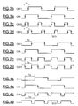
- Figures 2a to 2d respectively illustrate the four CLK, CLK1, CLK2 and CLK3 signals timing diagrams for a value of the delay Td making it possible ideally to obtain a 50% duty cycle for the CLK2 output clock signal.
- the value of the delay Td can vary one way or the other.
- FIGS. 3a - 3d show the time diagrams of these four clock signals in the case where the delay Td is less than the ideal value. So we see in this case that the duty cycle of the CLK2 output signal is less than 50%. It is therefore necessary to increase the value of the delay Td.
- the value too late of this delay and therefore, the too low value of the ratio cyclic translates, when sampling the second signal CLK3 delayed on the rising edges of the CLK incident signal by a null value of this CLK3 signal, null value which is stored in the second flip-flop FF2 and which constitutes one of the signal values sampled SCH.
- this zero value of the signal SCH means that the falling edge of the CLK3 signal has already occurred (which confirms the too low value of the delay Td), therefore too early by compared to the ideal case.
- Figures 4a - 4d illustrate the case where the value of the delay Td is too high which leads to too high a duty cycle for CLK2 output signal.
- the value "1" of signal CLK3 (which represents the other value of signal SCH) is present in the flip-flop FF2. This means that, compared to the ideal case, the falling edge of the CLK3 signal does not has not yet occurred which is a sign of too great a Td delay which should therefore be reduced.
- the sampled signal SCH will then be delivered to the means modulation so that these process the signal SEL modulation controlling the MX1 multiplexers of the two cells CEL1 and CEL 2.
- the signal of modulation SEL will act on the multiplexer MX1 to increase the number of delay elements ERj of each delay cell, and thus increasing the value of the delay Td.
- the signal SEL will control the multiplexer MX1 of each cell so as to reduce the number delay elements ERj connected between the input and the output of each delay cell, thereby decreasing the overall value Td of the delay.
- the modulation means comprise a control stage ETC having a control input EC1 receiving the signal SCH and an output BS5 delivering the modulation signal SEL.
- This floor of ETC command actually includes here incrementing means / MID decrement with a BE4 input looped back to the output BS5 of the control stage.
- the EC1 input is then the input of control of these MID means.
- These also include a BS4 output connected to one of the inputs of a DX duplexer whose output is connected to the input of a BCS type D output rocker. This BCS flip-flop forms the BS5 output of the control stage.
- the other DX duplexer input is also looped back to the BS5 output.
- SCN saturation means receive on the one hand the sampled signal SCH and, on the other hand, the output signal SAX delivered by the MID increment / decrement means. The output of these saturation means controls the DX duplexer.
- MDF frequency division means classic structure, and of which an embodiment based on two type D flip-flops and two inverters is illustrated in FIG. 1, are connected between the BEE input terminal of the doubling block of frequency (so as to receive the incident signal CLK), and the input of control of the additional BCS scale.
- the incrementation means / MID decrementation carried out conventionally from doors logic, increment or decrement the current value of the signal of modulation SEL which is present, by loopback, on input BE4 of these MID means.
- the SCN saturation means also produced so classic by means of logic gates, allow, in combination with the DX duplexer, to avoid an overflow. Indeed, if the value of the modulation signal SEL at input BE4 of the MID means, has already reaches its maximum value and the SCH signal requests a increment, the SAX output signal delivered by the MID means does not must not be valid because there would then be an overflow. In this case, the SCN saturation means control the DX duplexer on its input "1" so as to deliver at input of the BCS flip-flop, the old value of the SEL modulation signal. It is of course the same if the current value of the modulation signal SEL has already reached its value minimum and that the SCH signal requires decrementation.
- the control of the MX1 multiplexers of the two cells delay is synchronized at the output of the ETC control stage so to perfectly master the moment when adding or removing of a delay element ERj will actually take place in each delay cell.
- the ECH sampling means introduce a delay of two CLK clocks in the loop due to the presence of the two flip-flops FF1 and FF2. If we validated the update of the delay value in each delay cell at the frequency of the incident clock signal CLK, on would then obtain maximum oscillation on either side of the ideal position (50%) equivalent to two steps of elementary delay, i.e. twice the propagation time through an element ERi delay.
- the presence of MDF frequency division means and the BCS output toggle validates the update of the SEL modulation signal at a quarter of the frequency of the incident signal CLK, which allows the oscillation to be limited to one delay step.
- the length of the signal propagation path of SEL modulation up to multiplexers MX1 is such that the MX1 multiplexers are positioned before the signal edge incident had time to spread to the first element of delay ERj. This is generally the case with the techniques of realization and the components conventionally used in circuits integrated.
- the value sampled by the first flip-flop FF1 is advantageously recovery by a second flip-flop FF2 also controlled by the CLK incident signal.
- the number of delay elements ERi and ERj of each delay cell will determine the minimum delays and maximum that can be achieved. They are therefore chosen so as to suitable for the extreme cases expected, that is to say so that generate the correct pulse width on the output signal to have a duty cycle close to 50% in all conditions of operation.
- SCN saturation means by appropriately adjusting the number delay elements in each cell, (if necessary by providing a voluntarily too many delay elements connectable and disconnectable) so as to avoid the risks of saturation.
Landscapes
- Physics & Mathematics (AREA)
- Nonlinear Science (AREA)
- Pulse Circuits (AREA)
- Stabilization Of Oscillater, Synchronisation, Frequency Synthesizers (AREA)
- Manipulation Of Pulses (AREA)
Abstract
Description
- la figure 1 illustre de façon schématique un mode de réalisation d'un dispositif doubleur de fréquence selon l'invention et permettant une mise en oeuvre du procédé selon l'invention, et
- les figures 2a - 2d, 3a - 3d et 4a - 4d représentent des chronogrammes temporels permettant d'illustrer différents cas de fonctionnement du dispositif de la figure 1.
Claims (10)
- Procédé de doublement de la fréquence d'un signal d'horloge incident, caractérisé par le fait qu'on retarde le signal d'horloge incident (CLK) d'un premier retard variable (Td), on génère à partir de ce premier signal retardé (CLK1), du signal d'horloge incident (CLK)et d'une fonction logique du type OU EXCLUSIF (PL), un signal d'horloge de sortie (CLK2) de fréquence double de celle du signal d'entrée, on compare le rapport cyclique du signal de sortie à une valeur de référence prédéterminée et on module la valeur du premier retard (Td) en fonction du résultat de la comparaison, de façon à obtenir un signal d'horloge de sortie de fréquence double et à rapport cyclique contrôlé.
- Procédé selon la revendication 1, caractérisé par le fait que dans l'étape de comparaison du rapport cyclique, on retarde le signal de sortie (CLK2) d'un deuxième retard variable (Td) identique au premier retard de façon à obtenir un deuxième signal retardé et on échantillonne ce deuxième signal retardé en utilisant le signal incident (CLK), et par le fait qu'on module la valeur du premier et du deuxième retards en fonction de la valeur du signal échantillonné (SCH).
- Procédé selon la revendication 1 ou 2, caractérisé par le fait qu'on réalise chaque retard variable par une succession de retards élémentaires (ERi, ERj) dont le nombre est variable, et par le fait qu'on module la valeur dudit retard en incrémentant ou en décrémentant le nombre de retards élémentaires dans ladite succession.
- Procédé selon l'une des revendications précédentes, caractérisé par le fait qu'on module la valeur de chaque retard (Td) moins fréquemment que l'obtention du résultat de ladite comparaison du rapport cyclique du signal de sortie (CLK2).
- Dispositif de multiplication de la fréquence d'un signal d'horloge incident, caractérisé par le fait qu'il comprend au moins un bloc doubleur de fréquence comportant une borne d'entrée (BEE) pour le signal incident (CLK), une première cellule de retard variable (CEL1) reliée à ladite entrée, une porte OU EXCLUSIF (PL) dont une entrée est reliée à la sortie de la première cellule de retard (CEL1), dont l'autre entrée est reliée à ladite borne d'entrée (BEE), et dont la sortie est apte à délivrer un signal d'horloge de sortie (CLK2) de fréquence doublée par rapport à celle du signal incident, des moyens de comparaison (CEL2, ECH) pour comparer le rapport cyclique du signal de sortie à une valeur de référence prédéterminée et des moyens de modulation (ETC) pour moduler la valeur du premier retard en fonction du résultat de la comparaison.
- Dispositif selon la revendication 5, caractérisé par le fait que les moyens de comparaison comprennent une deuxième cellule de retard variable (CEL2), identique à la première cellule de retard variable (CEL1), reliée à la sortie de la porte OU EXCLUSIF, et délivrant un deuxième signal retardé (CLK3), des moyens d'échantillonnage (ECH) du deuxième signal retardé, reliés à la sortie de la deuxième cellule de retard, commandés par le signal incident et délivrant un signal échantillonné binaire(SCH), et par le fait que les moyens de modulation comprennent un étage de commande (ETC) possédant une entrée (EC1) recevant le signal échantillonné binaire, une sortie (BSS) délivrant un signal de modulation (SEL) à la première et à la deuxième cellules de retard de façon à augmenter ou à diminuer la valeur du retard (Td) en fonction de la valeur du signal échantillonné binaire.
- Dispositif selon la revendication 6, caractérisé par le fait que l'étage de commande (ETC) comprend des moyens d'incrémentation/décrémentation (MID) possédant une entrée de commande (EC1) reliée à l'entrée (EC1) de l'étage de commande, une entrée (BE4) reliée à la sortie de l'étage de commande et une sortie reliée à la sortie de l'étage de commande, les moyens d'incrémentation/décréinentation (MID) étant aptes à incrémenter ou à décrémenter le signal de modulation (CEL) en fonction de la valeur du signal échantillonné binaire, et par le fait que chaque cellule de retard comporte une succession d'élements de retard cascadés (ERi, ERj) dont les sorties respectives de certains au moins d'entre eux (ERj) sont reliées aux entreés d'un multiplexeur (MX1) commandé par le signal de modulation, la sortie du multplexeur étant reliée à la sortie de ladite cellule de retard.
- Dispositif selon la revendication 6 ou 7, caractérisé par le fait que les moyens d'échantillonnage comprennent deux bascules (FF1, FF2) connectées en série et commandées toutes deux par le signal incident.
- Dispositif selon la revendication 7 ou 8, caractérisé par le fait que l'étage de commande des moyens de modulation comprend un sous-étage diviseur de fréquence (MDF) recevant le signal incident (CLK1) et délivrant un signal de commande auxiliaire ayant une fréquence égale à un sous-multiple prédéterminé de la fréquence du signal incident, et une bascule de sortie (BCS) dont l'entrée est reliée à la sortie des moyens d'incrémentation/décrémentation, dont la sortie est reliée à la sortie de l'étage de commande des moyens de modulation, et dont l'entrée de commande reçoit le signal de commande auxiliaire.
- Dispositif selon l'une des revendications 5 à 9, caractérisé par le fait qu'il comprend plusieurs blocs doubleurs de fréquence connectés en série.
Applications Claiming Priority (2)
| Application Number | Priority Date | Filing Date | Title |
|---|---|---|---|
| FR9709022 | 1997-07-16 | ||
| FR9709022A FR2766305B1 (fr) | 1997-07-16 | 1997-07-16 | Procede de multiplication de la frequence d'un signal d'horloge avec controle du rapport cyclique, et dispositif correspondant |
Publications (2)
| Publication Number | Publication Date |
|---|---|
| EP0892497A1 true EP0892497A1 (fr) | 1999-01-20 |
| EP0892497B1 EP0892497B1 (fr) | 2004-11-03 |
Family
ID=9509277
Family Applications (1)
| Application Number | Title | Priority Date | Filing Date |
|---|---|---|---|
| EP98401706A Expired - Lifetime EP0892497B1 (fr) | 1997-07-16 | 1998-07-06 | Procédé de multiplication de la fréquence d'un signal d'horloge avec contrôle du rapport cyclique, et dispositif correspondant. |
Country Status (4)
| Country | Link |
|---|---|
| US (1) | US6091270A (fr) |
| EP (1) | EP0892497B1 (fr) |
| DE (1) | DE69827325T2 (fr) |
| FR (1) | FR2766305B1 (fr) |
Families Citing this family (4)
| Publication number | Priority date | Publication date | Assignee | Title |
|---|---|---|---|---|
| US6664833B1 (en) | 2000-11-20 | 2003-12-16 | Intersil Americas, Inc. | Dual-edge function clock generator and method of deriving clocking signals for executing reduced instruction sequences in a re-programmable I/O interface |
| US6456126B1 (en) * | 2001-05-25 | 2002-09-24 | Xilinx, Inc. | Frequency doubler with polarity control |
| US6597213B1 (en) * | 2002-04-03 | 2003-07-22 | Applied Micro Circuits Corporation | Cascadable frequency doubler having stable operation over varied manufacturing processes and environmental operating conditions |
| US7123063B2 (en) * | 2004-04-28 | 2006-10-17 | Broadcom Corporation | Supply tracking clock multiplier |
Citations (3)
| Publication number | Priority date | Publication date | Assignee | Title |
|---|---|---|---|---|
| US4799022A (en) * | 1986-11-07 | 1989-01-17 | Mitel Corporation | Frequency doubler with duty cycle monitor means |
| EP0441684A1 (fr) * | 1990-02-06 | 1991-08-14 | Bull S.A. | Circuit verrouillé en phase et multiplieur de fréquence en résultant |
| US5514990A (en) * | 1993-12-27 | 1996-05-07 | Kabushiki Kaisha Toshiba | Frequency multiplier circuit |
Family Cites Families (3)
| Publication number | Priority date | Publication date | Assignee | Title |
|---|---|---|---|---|
| US4710653A (en) * | 1986-07-03 | 1987-12-01 | Grumman Aerospace Corporation | Edge detector circuit and oscillator using same |
| JPH04329710A (ja) * | 1991-04-30 | 1992-11-18 | Nec Corp | 2逓倍回路 |
| JP3688392B2 (ja) * | 1996-05-31 | 2005-08-24 | 三菱電機株式会社 | 波形整形装置およびクロック供給装置 |
-
1997
- 1997-07-16 FR FR9709022A patent/FR2766305B1/fr not_active Expired - Fee Related
-
1998
- 1998-05-22 US US09/083,549 patent/US6091270A/en not_active Expired - Fee Related
- 1998-07-06 DE DE69827325T patent/DE69827325T2/de not_active Expired - Fee Related
- 1998-07-06 EP EP98401706A patent/EP0892497B1/fr not_active Expired - Lifetime
Patent Citations (3)
| Publication number | Priority date | Publication date | Assignee | Title |
|---|---|---|---|---|
| US4799022A (en) * | 1986-11-07 | 1989-01-17 | Mitel Corporation | Frequency doubler with duty cycle monitor means |
| EP0441684A1 (fr) * | 1990-02-06 | 1991-08-14 | Bull S.A. | Circuit verrouillé en phase et multiplieur de fréquence en résultant |
| US5514990A (en) * | 1993-12-27 | 1996-05-07 | Kabushiki Kaisha Toshiba | Frequency multiplier circuit |
Non-Patent Citations (1)
| Title |
|---|
| "DOUBLE FREQUENCY CLOCK GENERATOR", IBM TECHNICAL DISCLOSURE BULLETIN, vol. 34, no. 3, 1 August 1991 (1991-08-01), pages 55 - 57, XP000210447 * |
Also Published As
| Publication number | Publication date |
|---|---|
| DE69827325D1 (de) | 2004-12-09 |
| US6091270A (en) | 2000-07-18 |
| EP0892497B1 (fr) | 2004-11-03 |
| FR2766305A1 (fr) | 1999-01-22 |
| DE69827325T2 (de) | 2005-05-04 |
| FR2766305B1 (fr) | 2004-01-02 |
Similar Documents
| Publication | Publication Date | Title |
|---|---|---|
| EP0645888B1 (fr) | Ligne à retard numérique | |
| EP0441684B1 (fr) | Circuit verrouillé en phase et multiplieur de fréquence en résultant | |
| FR2709624A1 (fr) | Synthétiseur de fréquence. | |
| FR2752312A1 (fr) | Procede et circuit permettant d'ajuster dynamiquement la tension d'alimentation et, ou bien, la frequence du signal d'horloge dans un circuit numerique | |
| FR2668669A1 (fr) | Circuit et procede de generation de signaux de temps. | |
| FR2787651A1 (fr) | Detecteur numerique de frequence de phase | |
| EP0190730A1 (fr) | Dispositif de distribution d'horloge tripliquée, chaque signal d'horloge comportant un signal de synchronisation | |
| WO2003032495A1 (fr) | Circuit compteur diviseur double mode a phase commutee pour un synthetiseur de frequence | |
| FR2728118A1 (fr) | Comparateur de phase entre un signal numerique et un signal d'horloge, et boucle a verrouillage de phase correspondante | |
| EP0892497B1 (fr) | Procédé de multiplication de la fréquence d'un signal d'horloge avec contrôle du rapport cyclique, et dispositif correspondant. | |
| FR2939985A1 (fr) | Circuit integrateur a multifenetrage temporel | |
| FR2781942A1 (fr) | Procede d'integration et circuit d'integration offrant un rapport signal-bruit ameliore, ainsi qu'oscillateur commande par tension et convertisseur frequence-tension employant ce circuit d'integration | |
| EP0670629A1 (fr) | Dispositif oscillateur verrouillé en phase | |
| FR2851095A1 (fr) | Boucle a verrouillage de phase integree de taille reduite | |
| EP4038476B1 (fr) | Dispositif de generation d'une tension d'alimentation / polarisation et d'un signal d'horloge pour un circuit numerique synchrone | |
| FR2773925A1 (fr) | Synthetiseur de frequence a boucle d'asservissement en phase avec circuit de detection d'asservissement | |
| EP3048730B1 (fr) | Dispositif de synthèse de fréquence à boucle de rétroaction | |
| EP1606880B1 (fr) | Diviseur de frequence a taux de division variable | |
| EP0246135B1 (fr) | Détécteur de phase et de fréquence, et son utilisation dans une boucle à verrouillage de phase | |
| FR2770704A1 (fr) | Circuit verrouille en phase | |
| EP3764546B1 (fr) | Dispositif de synthèse de fréquence à boucle de rétroaction | |
| EP1133060A1 (fr) | Boucle à verrouillage de phase permettant de générer un signal de référence ayant une grande pureté spectrale | |
| EP0218508A1 (fr) | Générateur de fréquences à variation rapide | |
| EP1113579A1 (fr) | Procédé pour diviser la fréquence d'un signal | |
| EP3953770B1 (fr) | Micro-horloge atomique du type fonctionnant dans un regime impulsionnel |
Legal Events
| Date | Code | Title | Description |
|---|---|---|---|
| PUAI | Public reference made under article 153(3) epc to a published international application that has entered the european phase |
Free format text: ORIGINAL CODE: 0009012 |
|
| AK | Designated contracting states |
Kind code of ref document: A1 Designated state(s): DE FR GB IT |
|
| AX | Request for extension of the european patent |
Free format text: AL;LT;LV;MK;RO;SI |
|
| 17P | Request for examination filed |
Effective date: 19990201 |
|
| AKX | Designation fees paid |
Free format text: DE FR GB IT |
|
| RAP1 | Party data changed (applicant data changed or rights of an application transferred) |
Owner name: STMICROELECTRONICS S.A. |
|
| 17Q | First examination report despatched |
Effective date: 20030410 |
|
| GRAP | Despatch of communication of intention to grant a patent |
Free format text: ORIGINAL CODE: EPIDOSNIGR1 |
|
| GRAS | Grant fee paid |
Free format text: ORIGINAL CODE: EPIDOSNIGR3 |
|
| GRAA | (expected) grant |
Free format text: ORIGINAL CODE: 0009210 |
|
| AK | Designated contracting states |
Kind code of ref document: B1 Designated state(s): DE FR GB IT |
|
| REG | Reference to a national code |
Ref country code: GB Ref legal event code: FG4D Free format text: NOT ENGLISH |
|
| GBT | Gb: translation of ep patent filed (gb section 77(6)(a)/1977) | ||
| REF | Corresponds to: |
Ref document number: 69827325 Country of ref document: DE Date of ref document: 20041209 Kind code of ref document: P |
|
| PGFP | Annual fee paid to national office [announced via postgrant information from national office to epo] |
Ref country code: FR Payment date: 20050708 Year of fee payment: 8 |
|
| PLBE | No opposition filed within time limit |
Free format text: ORIGINAL CODE: 0009261 |
|
| STAA | Information on the status of an ep patent application or granted ep patent |
Free format text: STATUS: NO OPPOSITION FILED WITHIN TIME LIMIT |
|
| 26N | No opposition filed |
Effective date: 20050804 |
|
| PGFP | Annual fee paid to national office [announced via postgrant information from national office to epo] |
Ref country code: DE Payment date: 20060629 Year of fee payment: 9 |
|
| PGFP | Annual fee paid to national office [announced via postgrant information from national office to epo] |
Ref country code: IT Payment date: 20060731 Year of fee payment: 9 |
|
| REG | Reference to a national code |
Ref country code: FR Ref legal event code: ST Effective date: 20070330 |
|
| PGFP | Annual fee paid to national office [announced via postgrant information from national office to epo] |
Ref country code: GB Payment date: 20070627 Year of fee payment: 10 |
|
| PG25 | Lapsed in a contracting state [announced via postgrant information from national office to epo] |
Ref country code: FR Free format text: LAPSE BECAUSE OF NON-PAYMENT OF DUE FEES Effective date: 20060731 Ref country code: DE Free format text: LAPSE BECAUSE OF NON-PAYMENT OF DUE FEES Effective date: 20080201 |
|
| GBPC | Gb: european patent ceased through non-payment of renewal fee |
Effective date: 20080706 |
|
| PG25 | Lapsed in a contracting state [announced via postgrant information from national office to epo] |
Ref country code: GB Free format text: LAPSE BECAUSE OF NON-PAYMENT OF DUE FEES Effective date: 20080706 |
|
| PG25 | Lapsed in a contracting state [announced via postgrant information from national office to epo] |
Ref country code: IT Free format text: LAPSE BECAUSE OF NON-PAYMENT OF DUE FEES Effective date: 20070706 |