EP0892592A2 - Konstruktion zur Montage eines elektronischen Bauelementes auf einem flexiblen Substrat - Google Patents
Konstruktion zur Montage eines elektronischen Bauelementes auf einem flexiblen Substrat Download PDFInfo
- Publication number
- EP0892592A2 EP0892592A2 EP98305617A EP98305617A EP0892592A2 EP 0892592 A2 EP0892592 A2 EP 0892592A2 EP 98305617 A EP98305617 A EP 98305617A EP 98305617 A EP98305617 A EP 98305617A EP 0892592 A2 EP0892592 A2 EP 0892592A2
- Authority
- EP
- European Patent Office
- Prior art keywords
- electronic component
- flexible substrate
- clamping member
- clamping
- electrode
- Prior art date
- Legal status (The legal status is an assumption and is not a legal conclusion. Google has not performed a legal analysis and makes no representation as to the accuracy of the status listed.)
- Granted
Links
Images









Classifications
-
- H—ELECTRICITY
- H05—ELECTRIC TECHNIQUES NOT OTHERWISE PROVIDED FOR
- H05K—PRINTED CIRCUITS; CASINGS OR CONSTRUCTIONAL DETAILS OF ELECTRIC APPARATUS; MANUFACTURE OF ASSEMBLAGES OF ELECTRICAL COMPONENTS
- H05K3/00—Apparatus or processes for manufacturing printed circuits
- H05K3/30—Assembling printed circuits with electric components, e.g. with resistors
- H05K3/32—Assembling printed circuits with electric components, e.g. with resistors electrically connecting electric components or wires to printed circuits
- H05K3/325—Assembling printed circuits with electric components, e.g. with resistors electrically connecting electric components or wires to printed circuits by abutting or pinching; Mechanical auxiliary parts therefor
- H05K3/326—Assembling printed circuits with electric components, e.g. with resistors electrically connecting electric components or wires to printed circuits by abutting or pinching; Mechanical auxiliary parts therefor the printed circuit having integral resilient or deformable parts, e.g. tabs or parts of flexible circuits
-
- H—ELECTRICITY
- H05—ELECTRIC TECHNIQUES NOT OTHERWISE PROVIDED FOR
- H05K—PRINTED CIRCUITS; CASINGS OR CONSTRUCTIONAL DETAILS OF ELECTRIC APPARATUS; MANUFACTURE OF ASSEMBLAGES OF ELECTRICAL COMPONENTS
- H05K3/00—Apparatus or processes for manufacturing printed circuits
- H05K3/30—Assembling printed circuits with electric components, e.g. with resistors
-
- H—ELECTRICITY
- H05—ELECTRIC TECHNIQUES NOT OTHERWISE PROVIDED FOR
- H05K—PRINTED CIRCUITS; CASINGS OR CONSTRUCTIONAL DETAILS OF ELECTRIC APPARATUS; MANUFACTURE OF ASSEMBLAGES OF ELECTRICAL COMPONENTS
- H05K7/00—Constructional details common to different types of electric apparatus
- H05K7/02—Arrangements of circuit components or wiring on supporting structure
- H05K7/12—Resilient or clamping means for holding component to structure
-
- H—ELECTRICITY
- H05—ELECTRIC TECHNIQUES NOT OTHERWISE PROVIDED FOR
- H05K—PRINTED CIRCUITS; CASINGS OR CONSTRUCTIONAL DETAILS OF ELECTRIC APPARATUS; MANUFACTURE OF ASSEMBLAGES OF ELECTRICAL COMPONENTS
- H05K1/00—Printed circuits
- H05K1/18—Printed circuits structurally associated with non-printed electric components
- H05K1/189—Printed circuits structurally associated with non-printed electric components characterised by the use of flexible or folded printed circuits
-
- H—ELECTRICITY
- H05—ELECTRIC TECHNIQUES NOT OTHERWISE PROVIDED FOR
- H05K—PRINTED CIRCUITS; CASINGS OR CONSTRUCTIONAL DETAILS OF ELECTRIC APPARATUS; MANUFACTURE OF ASSEMBLAGES OF ELECTRICAL COMPONENTS
- H05K2201/00—Indexing scheme relating to printed circuits covered by H05K1/00
- H05K2201/09—Shape and layout
- H05K2201/09009—Substrate related
- H05K2201/09081—Tongue or tail integrated in planar structure, e.g. obtained by cutting from the planar structure
-
- H—ELECTRICITY
- H05—ELECTRIC TECHNIQUES NOT OTHERWISE PROVIDED FOR
- H05K—PRINTED CIRCUITS; CASINGS OR CONSTRUCTIONAL DETAILS OF ELECTRIC APPARATUS; MANUFACTURE OF ASSEMBLAGES OF ELECTRICAL COMPONENTS
- H05K2201/00—Indexing scheme relating to printed circuits covered by H05K1/00
- H05K2201/10—Details of components or other objects attached to or integrated in a printed circuit board
- H05K2201/10227—Other objects, e.g. metallic pieces
- H05K2201/10393—Clamping a component by an element or a set of elements
-
- H—ELECTRICITY
- H05—ELECTRIC TECHNIQUES NOT OTHERWISE PROVIDED FOR
- H05K—PRINTED CIRCUITS; CASINGS OR CONSTRUCTIONAL DETAILS OF ELECTRIC APPARATUS; MANUFACTURE OF ASSEMBLAGES OF ELECTRICAL COMPONENTS
- H05K2201/00—Indexing scheme relating to printed circuits covered by H05K1/00
- H05K2201/10—Details of components or other objects attached to or integrated in a printed circuit board
- H05K2201/10613—Details of electrical connections of non-printed components, e.g. special leads
- H05K2201/10621—Components characterised by their electrical contacts
- H05K2201/10636—Leadless chip, e.g. chip capacitor or resistor
-
- H—ELECTRICITY
- H05—ELECTRIC TECHNIQUES NOT OTHERWISE PROVIDED FOR
- H05K—PRINTED CIRCUITS; CASINGS OR CONSTRUCTIONAL DETAILS OF ELECTRIC APPARATUS; MANUFACTURE OF ASSEMBLAGES OF ELECTRICAL COMPONENTS
- H05K2201/00—Indexing scheme relating to printed circuits covered by H05K1/00
- H05K2201/10—Details of components or other objects attached to or integrated in a printed circuit board
- H05K2201/10613—Details of electrical connections of non-printed components, e.g. special leads
- H05K2201/10621—Components characterised by their electrical contacts
- H05K2201/10651—Component having two leads, e.g. resistor, capacitor
-
- Y—GENERAL TAGGING OF NEW TECHNOLOGICAL DEVELOPMENTS; GENERAL TAGGING OF CROSS-SECTIONAL TECHNOLOGIES SPANNING OVER SEVERAL SECTIONS OF THE IPC; TECHNICAL SUBJECTS COVERED BY FORMER USPC CROSS-REFERENCE ART COLLECTIONS [XRACs] AND DIGESTS
- Y02—TECHNOLOGIES OR APPLICATIONS FOR MITIGATION OR ADAPTATION AGAINST CLIMATE CHANGE
- Y02P—CLIMATE CHANGE MITIGATION TECHNOLOGIES IN THE PRODUCTION OR PROCESSING OF GOODS
- Y02P70/00—Climate change mitigation technologies in the production process for final industrial or consumer products
- Y02P70/50—Manufacturing or production processes characterised by the final manufactured product
Definitions
- This invention relates to a construction for mounting an electronic component on a flexible substrate.
- soldering or cold soldering technique has been used, for allowing electrode portions of an electronic component of a chip type to be connected to a circuit pattern which has been formed by etching a copper foil disposed on a flexible substrate.
- soldering cream is printed on a flexible substrate.
- an electronic component of a chip type is placed on the soldering cream by means of an automatic mounting machine.
- the flexible substrate is directed into a heating furnace so as to cause the electronic component to be soldered on the flexible substrate.
- a U. V. curable adhesive is applied on the electronic component so as to encapsulate the electronic component.
- the thus encapsulated electronic component is directed into a U. V. irradiation furnace so as to be cured therein for the purpose of reinforcement.
- a problem regarding adhesive property is caused, in contrast to the circuit pattern formed by etching a copper foil.
- a conductive adhesive of a hot melt type is conventionally used in place of a solder. It is also necessary to use a conductive adhesive, when a film having a low heat-resistive temperature (for example, polyethylene terephthalate (PET) film) is used as a flexible substrate.
- PET polyethylene terephthalate
- a conductive adhesive is printed on the flexible substrate and then dried.
- An electronic component is placed on the conductive adhesive by means of an automatic mounting machine. Thereafter, the flexible substrate and the electronic component are heated and compressed together, so as to cause the conductive adhesive to be melt, whereby the flexible substrate and the electronic component are connected together.
- the flexible substrate mounted thereon the electronic components may directed into a heating furnace or U. V. irradiation furnace, so as to cause the electronic components to be efficiently connected at one time.
- the mounting construction comprises a flexible substrate including a flexible sheet, bendable electrode pattern forming portions formed on the flexible sheet, and electrode patterns formed on the electrode pattern forming portions, an electronic component having electrode portions, and a clamping member having clamping pieces for clamping the electronic component therebetween.
- the electrode pattern forming portions are deflected, so as to cause the electrode patterns to be contacted with the electrode portions of the electronic component placed on the flexible substrate. By this, the electronic component is clamped by the clamping pieces of the clamping member through the deflected electrode pattern forming portions.
- the electronic component may be mounted on the flexible substrate by means of a mechanical clamping means.
- This facilitate easy mounting of the electronic component on the flexible substrate, and eliminates the use of a heating furnace or U. V. irradiation furnace during mounting of the electronic component on the flexible substrate.
- Production efficiency may be improved, even when a smaller number of electronic components are mounted on a flexible substrate.
- Production equipment such as a heating furnace may also be eliminated, thus reducing production cost.
- the electronic component and the electrode pattern forming portions of the flexible substrate are clamped by a clamping member, the electronic component may be reliably secured on the flexible substrate, without using additional adhesives for the purpose of reinforcement.
- the clamping member is formed from a resilient metal plate.
- the metal plate is bent, at its opposite sides, into a predetermined configuration, so that the bent opposite sides serve as the clamping pieces.
- the clamping member is formed with guide rugs.
- the guide rugs are adapted to be upstandingly extended through the flexible substrate.
- the clamping member may be properly positioned relative to the flexible substrate. It is also noted that the electronic component or the portions of the clamping member, by which the electronic component is clamped, is prevented from directly contacted by another member, so that the electronic component may be mounted more stably.
- the clamping member is formed with presser portions which tend to urge the clamping pieces to their open positions.
- the flexible substrate is formed, at its portion which is not clamped by the clamping member, with an insulating layer having a predetermined thickness.
- the electronic component with the lower surface thereof facing upwardly, may be mounted on the flexible substrate and clamped by the clamping pieces of the clamping member, when the electrode portions of the electronic component is formed from a metal plate, which extends from a casing of the electronic component along the outer surface of the casing and is bent toward the lower surface of the casing.
- the electronic component may be easily and reliably mounted on the flexible substrate, without causing the clamping pieces to be opened to a substantial degree.
- the clamping pieces of the clamping member are formed by bending a resilient metal plate, at its opposite ends, into a predetermined configuration, while providing a positioning hole in the resilient metal plate at its center.
- the clamping member may be appropriately positioned relative to a push-up member, on which the clamping member is placed, when the clamping pieces of the clamping member are to be opened.
- the clamping pieces may be reliably opened.
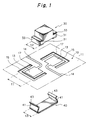
- Fig. 1 is an exploded perspective view showing the main portion of a construction in which an electronic component is mounted on a flexible substrate in accordance with a first embodiment of the invention.
- a flexible substrate 10 and an electronic component 30 are mechanically and electrically connected and secured relative to one another by means of a clamping member 40, as shown in Fig. 1.
- a clamping member 40 as shown in Fig. 1.
- the flexible substrate 10 is comprised of a synthetic resin film (for example, a flexible sheet made of PET) 11, and electrode patterns 13, 13 formed on the surface of the synthetic resin film 11.
- a notch 15 is formed which circumscribes the three sides of a respective electrode pattern 13, whereby an electrode pattern forming portion 17 of a tongue-like configuration is provided.
- the width t1 of each of the electrode pattern forming portions 17 and 17 is selected to be slightly larger than the width t2 of the electronic component 30.
- Each electrode pattern 13 is formed, together with a respective circuit pattern 14 leading out from a respective electrode pattern 13, by providing silver paste on the substrate by means of screen printing.
- the electronic component 30 is a light emitting diode.
- An electrode portion 33 is formed on the lower surface, the side surface and the upper surface of a protrusion 31 extending outwardly from each side of the electronic component.
- the electrode portions 33 and 33 may be formed by applying metal foil on the above-mentioned surfaces of the protrusion, or by means of metal plating.
- the clamping member 40 is formed by bending a resilient metal plate of a rectangular configuration at its opposite sides, so as to form clamping pieces 41 and 41.
- the clamping pieces 41 and 41 are bent into a position slightly inward of the vertical plane. Specifically, the clamping pieces 41 and 41 are bent to an angle more than 90 degrees.
- the top edge 43 of each of the clamping pieces 41 and 41 is bent in the opposite direction so as to be opened outwardly.
- the width t3 of the clamping member 40 is slightly smaller than the width t2 of the electronic component 30.
- the electronic component 30 When the electronic component 30 is to be mounted on the flexible substrate 10, the electronic component 30 is first placed on the flexible substrate 10 so that the electrode patterns 13 and 13 are connected respectively with the lower surfaces of the electrode portions 33 and 33. No material such as an adhesives or a solder is placed between the electrode patterns 13 and 13 and the lower surfaces of the electrode portions 33 and 33.
- the clamping member 40 is pushed upwardly from the rear-side surface of the flexible substrate 10.
- the electrode pattern forming portions 17 and 17 are deflected upwardly by means of the clamping pieces 41 and 41 of the clamping member 40, so as to be wound around a respective protrusion 31 of the electronic component 30, whereby the electronic component 30 is resiliently clamped.
- the electrode portions 33 and 33 of the electronic component 30 and the corresponding electrode pattern forming portions 17 and 17 are pressed and connected together, whereby mounting of the electronic component 30 is completed.
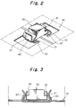
- Fig. 2 is a schematic perspective view showing the electronic component 30 having been mounted on the flexible substrate 10 in the above-mentioned manner.
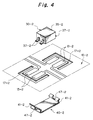
- Fig. 3 is a side sectional view of Fig. 2.
- the electrode pattern 13 and 13 formed on the flexible substrate 10 are urged against the corresponding electrode portions 33 and 33 of the electronic component 30 by means of the clamping pieces 41 and 41 of the clamping member 40.
- the flexible substrate 10 and the electronic component 30 are electrically and mechanically secured together in a positive manner.
- the width t1 (refer to Fig. 1) of each of the electrode forming portions 17 is selected to be greater than the width t3 of the clamping member 40, in order to securely prevent the clamping member 40, which is made of a conductive metal, from contacting directly with the electrode portions 33 of the electronic component 30, so as to eliminate any occurrence of short circuit by means of the clamping member 40.
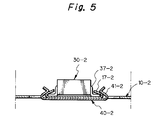
- Fig. 4 is a schematic exploded perspective view showing a second embodiment of the invention.
- Fig. 5 is a side sectional view showing an electronic component 30-2 mounted on a flexible substrate 10-2. This embodiment is different from the first embodiment by the construction of the electronic component 30-2, and the configuration of the flexible substrate 10-2 and the clamping member 40-2 having been modified in accordance with the construction of the electronic component 30-2.
- the electronic component 30-2 of this embodiment is a chip type diode array.
- the electronic component 30-2 includes a resin-encapsulated casing 35-2, and two electrode portions 37-2 of a metal plate protruding from each side surface of the casing 35-2.
- Clamping pieces 41-2 and 41-2 of a clamping member 40-2 are each divided into two sections by means of a respective slit 47-2.
- the electronic component 30-2 is placed on the flexible substrate 10-2. Then, the clamping member 40-2 is pushed upwardly from the rear-side surface of the flexible substrate 10-2. By this, the opposite electrode pattern forming portions 17-2 and 17-2 are deflected in the upward direction by means of the clamping pieces 41-2 and 41-2 of the clamping member 40-2, and wound around a respective electrode portion 37-2 of the electronic component 30-2. By this, the electronic component is resiliently clamped.
- Each clamping piece 41-2 is divided into two sections by means of a respective slit 47-2, so as to cause the electrode portions 37-2 to be separately and securely clamped, whereby the electrode portions may be securely clamped regardless of any variation in thickness and length of the electrode portions 37-2, thus providing reliable connection therebetween.
- the electronic component 30 may be easily mounted on the flexible substrate 10, while at the same time eliminating the use of a heating furnace or U. V. irradiation furnace during mounting of the electronic component 30 on the flexible substrate 10.
- a heating furnace or U. V. irradiation furnace during mounting of the electronic component 30 on the flexible substrate 10.
- the electronic component 30 may be positively secured on the flexible substrate, thus obviating any additional reinforcing means such as adhesives.
- the clamping pieces 41 and 41 of the clamping member 40 are forcibly opened by means of the electrode portions 33 and 33 of the electronic component 30 when the clamping member 40 is attached to the electronic component 30.
- an increased load is undesirably applied to the electrode portions 33 and 33. This may cause the electrode portions 33 and 33 to be damaged.
- Embodiments to be explained below are intended to eliminate such a problem.
- Fig. 6 is a schematic exploded perspective view showing a mounting construction in which an electronic component is mounted on a flexible substrate according to a third embodiment of the invention.
- a flexible substrate 10-3 and an electronic component 30-3 are mechanically and electrically connected and secured together by means of a clamping member 40-3.
- a clamping member 40-3 Each component part will be explained below.
- the flexible substrate 10-3 includes a synthetic resin film (for example, a flexible sheet of PET) 11-3, and two electrode patterns 13-3 and 13-3 formed on the surface of the synthetic resin film 11-3.
- a notch 15-3 is formed in the synthetic resin film 11-3 so as to circumscribe the three peripheral sides of a respective electrode pattern 13-3.
- electrode pattern forming portions 17-3 and 17-3 of a tongue-like configuration are provided.
- electrode patterns 13-3 and 13-3 together with circuit patterns 14-3 and 14-3 leading out from the respective electrode patterns 13-3 and 13-3, have been formed by applying silver paste on the synthetic resin film using a screen printing.
- Insulation layers 21-3 and 21-3 are formed in the connection portions 19-3 and 19-3 at the proximal portions of the notches 15-3 and 15-3.
- the insulation layers 21-3 and 21-3 are formed by applying insulating paint on the connection portions 19-3 and 19-3 for several times using screen printing.
- the thickness of the insulating layers 21-3 and 21-3 is selected to be approximately 100 micrometers.
- the electronic component 30-3 is a light emitting diode and has an outer configuration of a convex shape. Electrode portions 33-3 and 33-3 are formed on the lower surface, the side surface and the upper surface of protrusions 31-3 and 31-3 extending outwardly from the opposite sides of the electronic component.
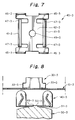
- the clamping member 40-3 includes a base portion 42-3 and a clamping pieces 41-3 at each side of the base portion, as shown in Figs. 6 and 7.
- the clamping pieces 41-3 and 41-3 are formed by bending the opposite sides of the resilient metal plate in the upward direction.
- the clamping member 40-3 also includes a connection portion 43-3 of a T-shaped configuration extending from each side different from the sides on which the clamping pieces 41-3 and 41-3 are formed.
- the outer edge of each of the connection portions 43-3 and 43-3 is bent at its opposite ends in the upward direction, so as to form, in total, four guide rugs 45-3 of a tongue-like configuration.
- each of the clamping pieces 41-3 and 41-3 is configured to have a width at its forward end which is greater than that at its proximal end.
- the width of the forward end of the clamping piece is selected to be greater than that of the electrode pattern forming portions 17-3 and 17-3 of the flexible substrate 10-3.
- the opposite end portions of the forward end serve as a presser portion 47-3.
- Each of the guide rugs 45-3 has a width t2 which is slightly smaller than the outer width t1 of the notches 15-3 and 15-3 formed in the flexible substrate 10-3.
- Each of the guide rugs 45-3 has a height which is slightly greater than the height of the clamping pieces 41-3 and the height of the electronic component 30-3.
- a positioning hole 49-3 is formed in the base portion 42-3 in its central portion.
- the electronic component 30-3 When the electronic component 30-3 is to be mounted on the flexible substrate 10-3, the electronic component 30-3 is first placed on the flexible substrate 30-3, as shown in Fig. 8, so that the electrode patterns 13-3 and 13-3 (see Fig. 6) and the lower surfaces of the electrode portions 33-3 and 33-3 are bonded together (no adhesive or solder is placed therebetween). At the same time, the clamping member 40-3 placed on a push-up member 50-3 is disposed directly blow the flexible substrate 10-3 mounted with the electronic component 30-3, as shown in Fig. 8. It is noted that a circular protrusion 53-3 at the central portion of the push-up member 50-3 has been inserted in the positioning hole 49-3 of the clamping member 40-3.
- the upper surface 51-3 of the push-up member 50-3 is curved into an arcuate configuration having a predetermined curvature.
- the four presser protrusions 55-3 (only two rearward presser protrusions are shown in Fig. 9) are moved from the upper side of the flexible substrate 10-3 through the notches 15-3, as shown in Fig. 9.
- the four presser portions 47-3 (refer to Figs. 6 and 7) of the clamping pieces 41-3 and 41-3 of the clamping member 40-3 are depressed, so that the clamping pieces 41-3 and 41-3 are opened outwardly.
- the base portion 42-3 of the clamping member 40-3 is deflected into a configuration the same as that of the upper surface 51-3 of the push-up member 50-3.
- the push-up member 50 is gradually pushed upwardly, as shown in Fig. 10. Since the head portion of the electronic component 30-3 is urged in the downward direction by means of a jig 60-3, the electrode pattern forming portions 17-3 and 17-3 are pushed upwardly by means of the clamping pieces 41-3 and 41-3, so as to be deflected to a position adjacent to a corresponding protrusion 31-3.
- the electronic component 30-3 is firmly and resiliently clamped by the clamping pieces 41-3 and 41-3 of the clamping member 40-3.
- the electrode portions 33-3 and 33-3 of the electronic component 30-3 and the electrode pattern forming portions 17-3 and 17-3 of the flexible substrate 10-3 are firmly compressed and connected together, whereby mounting of the electronic component 30-3 is completed.
- the electrode patterns 13-3 and 13-3 (refer to Fig. 6) are urged against the electrodes 33-3 and 33-3 respectively, so that the flexible substrate 10-3 and the electronic component 30-3 are electrically and mechanically secured together in firm and stable manner.
- the electronic component 30-3 may be slid in a direction (lateral direction) A shown by the arrow mark in Fig. 6, when an excessive force is applied to the electronic component in the direction A.
- the insulating layers 21-3 and 21-3 having a predetermined thickness are provided by printing at the locations where the electronic component 30-3 is to be slid.
- the electronic component 30-3, which is strongly urged against the flexible substrate 10-3 by means of the clamping member 40-3, is unable to get over the predetermined thickness of the insulating layers 21-3 and 21-3, so that lateral slidable movement of the electronic component 30-3 is securely prevented.
- the guide rugs 45-3 are provided for the two reasons mentioned below. First, the guide rugs 45-3 are contacted, on their outer surfaces, with the outer four edges 15a-3 (refer to Fig. 6) of the notches 15-3, so that the clamping member 40-3 may be maintained at an appropriate position at all time.
- the electronic component 30-3 or the clamping pieces 41-3 is only contacted with guide member 45-3, since the guide rugs 45-3 having a height greater than that of the electronic component 30-3 or the clamping pieces 41-3.
- the electronic component 30-3 or the clamping pieces 41-3 are not contacted by another member, whereby the electronic component 30-3 may be securely maintained in its mounted state.
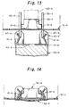
- Figs. 12 through 14 illustrate how an electronic component 30-4 is mounted on a flexible substrate 10-4 using a clamping member 40-4 according to a fourth embodiment of the invention.
- the clamping member 40-4 according to this embodiment is only different from the third embodiment by the fact that the base portion 42-4 is preliminarily bent into a configuration so that its opposite ends are raised toward the upward direction, as shown in Fig. 12. Thus, the clamping pieces 41-4 and 41-4 are inclined more inwardly as compared with the third embodiment.
- the clamping member 40-4 placed on a push-up member 50-4 is first disposed just below the flexible substrate 10-4 on which the electronic component 30-4 is mounted.
- the upper surface 51-4 of the push-up member 50-4 is formed in a flattened shaped.
- the clamping pieces 41-4 and 41-4 in an opened state are located at positions opposite to the protrusions 31-4 and 31-4 of the electronic component 30-4. Then, the push-up member 50-4 and the presser rugs 55-4 as well as the jig 60-4 are removed. By this, the electronic component 30-4 is firmly and securely held on the flexible substrate 10-4 by means of the clamping pieces 41-4 and 41-4, as shown in Fig. 14.
- a clamping member 40-5 may be provided, which includes, for example as shown in Fig. 15, presser portions 47-5 and a positioning hole 49-5, with the omission, for example, of the guide rugs 45-3 shown in Fig. 6.
- the position of the presser portions on the clamping member is not restricted to those shown in the above embodiments.
- the presser portions may be positioned desirably, provided that they are able to urge the clamping pieces into an opened configuration.
- presser portions 47-6 may be provided at four corners of the base portion 42-6, in place of the presser portions provided on the clamping pieces 41-6 and 41-6. In this case, the clamping pieces 41-6 and 41-6 may be opened by depressing the presser portions 47-6.
- a notch 70-6 is formed at a position inward of each presser portion 47-6, so that the clamping pieces 41-6 and 41-6 may be easily opened.
- Fig. 17 is a schematic exploded perspective view showing a mounting construction in which an electronic component is mounted on a flexible substrate according to a seventh embodiment of the invention.
- a flexible substrate 10-7 and an electronic component 30-7 are mechanically and electrically connected and secured together by means of a clamping member 40-76, as shown in Fig. 17.
- a clamping member 40-76 As shown in Fig. 17.
- the flexible substrate 10-7 includes a flexible sheet 11-7 made of a synthetic resin film (for example, PET film), and three electrode patterns 13-7 formed on the surface of the flexible sheet.
- a pair of notches 15-7 and 15-7 are formed, which circumscribe the periphery of the three electrode pattern 13-7, so as to form electrode pattern forming portions 17-7 and 17-7 of a tongue-like configuration.
- electrode patterns 13-7 are formed, together with circuit patterns 14-7 leading out from the respective electrode patterns 13-7, by providing silver paste on the flexible sheet by screen printing.
- Insulating layers 21-7 and 21-7 are formed on the connection portions 19-7 and 19-7 at the proximal portion of the notches 15-7 and 15-7 by means of a plurality of screen printing of insulating paint.
- the thickness of the insulating layers 21-7 and 21-7 is selected to be, for example, 100 micrometers.
- the electronic component 30-7 is a diode.
- the electrode component is shown in an up-side-down or inverted position.
- the electronic component 30-7 includes a casing 31-7 of a substantially rectangular parallelopiped configuration, and three electrode portions 33-7 made of a metal plate. One electrode portion is protruded from one outer surface of the casing, and the remaining two electrode portions are protruded from the other outer surface of the casing.
- each electrode portion 33-7 is formed by bending the metal plate, which protrudes from the outer surface 35-7 of the casing 31-7, along the outer surface 35-7 of the casing 31-7 toward the lower surface 37-7 of the casing 31-7, and then bending it into a substantially normal angle, so that the forward end of the metal plate extends outwardly along a plane substantially the same as that of the lower surface 37-7 of the casing 31-7.
- the clamping member 40-7 is formed from a resilient metal plate. Specifically, the opposite sides of the metal plate are bent into the upward direction, so as to form two clamping pieces 41-7 and 41-7 at opposite sides of the base portion 42-7. Presser portions 47-7 of a tongue-like configuration are formed at opposite ends of the upper side edge of each of the clamping pieces 41-7 and 41-7.
- Each presser portion 47-7 is bent so that its forward end is directed outwardly.
- a positioning hole 49-7 is formed in the base portion 42-7 at its center.
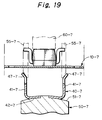
- the electronic component 30-7 When the electronic component 30-7 is to be mounted on the flexible substrate 10-7, the electronic component 30-7 in its inverted position (i. e., the lower surface 37-7 is faced upwardly) is first placed on the flexible substrate 10-7, as shown in Fig. 18. At the same time, the clamping member 40-7 mounted on a push-up member 50-7 is disposed immediately below the portion of the flexible substrate 10-7 on which the electronic component 30-7 is mounted. It is noted that a circular protrusion 53-7 at the center of the push-up member 50-7 is preliminarily inserted into the positioning hole 49-7 of the clamping member 40-7.
- the upper surface 51-7 of the push-up member 50-7 is curved into an arcuate configuration having a predetermined curvature.
- the push-up member 50-7 is gradually pushed upwardly, as shown in Fig. 20. Since the inverted electronic component 30-7 is depressed on its lower surface 37-7 by a jig 60-7, the electrode pattern forming portions 17-7 and 17-7 are displaced upwardly and deflected by the clamping pieces 41-7 and 41-7, so as to be located at positions outward of the electrode portions 33-7 and 33-7 of the electronic component 30-7.
- the clamping pieces 41-7 and 41-7 are opened, no excessive force is applied to the electrode portions 33-7 and 33-7, so that there is no risk of the electrode portions to be damaged. It is also noted that, since the lower surface 37-7 of the electronic component 30-7 is not strongly depressed by the jig 60-7, there is no risk of elements or devices within the electronic component 30-7 to be damaged. Specifically in the illustrated embodiment, the electronic component 30-7 is mounted in its inverted position. Thus, it is unnecessary for the protruding forward ends of the electrode portions 33-7 and 33-7 to get over the clamping pieces 41-7 and 41-7, so that the clamping pieces 41-7 and 41-7 need not to be significantly opened. Thus, mounting of the electronic component may be performed easily.
- the electronic component 30-7 is firmly and resiliently clamped by the clamping pieces 41-7 and 41-7 of the clamping member 40-7, as shown in Figs. 21 and 22.
- the electrode portions 33-7 and 33-7 of the electronic component 30-7 and the electrode pattern forming portions 17-7 and 17-7 of the flexible substrate 10-7 are strongly compressed and connected together, whereby mounting of the electronic component 30-7 is completed.
- the three electrode patterns 13-7 are urged in surface-to-surface contact against the outer surface of the respective electrode portions 33-7.
- the flexible substrate 10-7 and the electronic component 30-7 are electrically and mechanically secured together in a firm and secure manner.
- Figs. 23 through 25 illustrate how an electronic component 30-8 is mounted on a flexible substrate 10-7 using a clamping member 40-8 according to a eighth embodiment of the invention.
- the clamping member 40-8 according to the illustrated embodiment is only different from the above-mentioned seventh embodiment by the fact that the base portion 42-8 is preliminarily bent into a curved configuration so that its opposite ends are raised upwardly, as shown in Fig. 23.
- the clamping member 40-8 placed on a push-up member 50-8 is disposed immediately below the flexible substrate 10-8 on which the inverted electronic component 30-7 is mounted. It is noted that the upper surface 51-8 of the push-up member 50-8 is configured into a flattened form.
- FIG. 24 As in the case of the seventh embodiment, four presser portions 47-8 of the clamping member 40-8 are displaced by four presser rugs 55-8 (in Fig. 24, only rearward two are shown), as shown in Fig. 24.
- the clamping pieces 41-8 and 41-8 are opened outwardly, so that the base portion 42-8 of the clamping member 40-8 is urged against the upper surface 51-8 of the push-up member 50-8 into a flattened form.
- the push-up member 50-8 is gradually pushed upwardly, with the electrode component 30-8 being positioned by the jig 60-8, so that the opened clamping pieces 41-8 and 41-8 are located at positions outward of the corresponding electrode portions 33-8 and 33-8 of the electronic component 30-8.
- the electronic component 30-8 is firmly and positively secured to the flexible substrate 10-8 by means of the clamping pieces 41-8 and 41-8, as shown in Fig. 25.
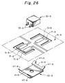
- Figs. 26 and 27 illustrate a ninth embodiment of the invention, wherein Fig. 26 is a schematic perspective view in an exploded fashion and Fig. 27 is a side sectional view in an assembled fashion.
- an electronic component 30-9 is mounted on a flexible substrate 10-9 in its normal posture, not an inverted posture.
- clamping pieces 41-9 and 41-9 of a clamping member 40-9 are sized and configured so as to cause electrode pattern forming portions 17-9 and 17-9 of the flexible substrate 10-9, as well as the forward ends of three electrode portions 33-9 (only two are shown in the figure) made of a metal plate of the electronic component 30-9, to be clamped therebetween.
- presser portions 47-9 and 47-9 extending in a tongue like configuration are formed at opposite ends of the upper side of each of the clamping pieces.
- the clamping member 40-9 placed on a push-up member (not shown) is first disposed immediately below the flexible substrate 10-9 on which the electronic component 30-9 is mounted. Then, the presser portions 47-9 are displaced by four presser rugs (not shown), so as to cause the clamping pieces 41-9 and 41-9 to be opened outwardly.
- the electrode pattern forming portions 17-9 and 17-9 are deflected by the clamping pieces 41-9 and 41-9, so that they are located at positions outward of the respective electrode portions 33-9 and 33-9.
- the electrode patterns 13-9 and the electrode portions 33-9 are electrically connected together.
- position of the presser portions on the clamping member is not restricted to those shown in relation to the above-mentioned embodiments.
- a presser portion 47-10 may be provided at each corner of the base portion 42-10, in place of the presser portions provided on the clamping pieces 41-10 and 41-10.
- the clamping pieces 41-10 and 41-10 may be opened when the presser portions 47-10 are depressed.
- Fig. 29 is a schematic exploded perspective view showing a mounting construction according to an eleventh embodiment of the invention in which an electronic component is mounted on a flexible substrate.
- Figs. 30 and 31 are a schematic perspective view and a schematic side sectional view respectively showing the mounting construction according to the eleventh embodiment of the invention in which an electronic component is mounted on a flexible substrate.
- a flexible substrate 10-11 and an electronic component 30-11 are mechanically and electrically connected and fixed with each other by means of a clamping member 40-11, as shown in Fig. 29.
- left-hand side three electrode portions 33-11 and right-hand side three electrode portions 33-11, each made of a metal plate, of the electronic component 30-11 are respectively placed on six electrode patterns 13-11 formed on the flexible substrate 10-11 by printing. Then, the flexible substrate 10-11 is placed on the clamping member 40. At this stage, bendable surfaces 27-11 and 27-11 formed by notches 15-11 and 15-11 in the flexible substrate 10-11 are bent in the upward direction by means of clamping pieces 41-11 and 41-11 on opposite ends of the clamping member 40-11. Since two slits 29-11 and 29-11 are formed in the flexible substrate 10-11, the bendable surfaces 27-11 and 27-11 may be easily bent.
- the clamping pieces 41-11 and 41-11 are bent so as to be urged against the electrode portions 33-11, as shown in Figs. 30 and 31.
- the electrode portions 33-11 are clamped between the flexible substrate 10-11 and the bendable surfaces 27-11, so as to be mechanically secured.
- the electrode portions 33-1 are urged against the electrode patterns 13-11, so as to be electrically connected therewith.
- two small holes 28-11 are in the flexible substrate loll, such that two small protrusions 48-11 on the clamping member 40-11 may be forcibly inserted therein.
- the two small protrusions 48-11 are provided, in order to prevent the electronic component 30-11 from slidably moving in a direction in which it is not clamped or restricted by the clamping member 40-11.
- the electronic component may be, for example, an electronic component having a function other than that shown in connection with the above-mentioned embodiment. It is also noted that various modifications may of course be made, for example, to the configuration of the electronic component, the number or configuration of the electrode portions, the configuration of the clamping member, and the configuration of the electrode patterns or the electrode pattern forming portions formed on the flexible substrate.
- silver paste printed on the substrate is used as electrode patterns. It is noted, however, that copper foils formed on the substrate by etching or the like may be used as the electrode patterns.
- solder or adhesives may be combiningly used for the reinforcing purpose.
Landscapes
- Engineering & Computer Science (AREA)
- Microelectronics & Electronic Packaging (AREA)
- Manufacturing & Machinery (AREA)
- Metallurgy (AREA)
- Structures For Mounting Electric Components On Printed Circuit Boards (AREA)
- Electric Connection Of Electric Components To Printed Circuits (AREA)
- Structure Of Printed Boards (AREA)
Applications Claiming Priority (9)
| Application Number | Priority Date | Filing Date | Title |
|---|---|---|---|
| JP9208572A JP3052071B2 (ja) | 1997-07-16 | 1997-07-16 | 電子部品のフレキシブル基板取付構造 |
| JP208572/97 | 1997-07-16 | ||
| JP20857297 | 1997-07-16 | ||
| JP33797997 | 1997-11-20 | ||
| JP337979/97 | 1997-11-20 | ||
| JP09337979A JP3108746B2 (ja) | 1997-11-20 | 1997-11-20 | 電子部品のフレキシブル基板への取付構造及び取付方法 |
| JP36902797 | 1997-12-26 | ||
| JP369027/97 | 1997-12-26 | ||
| JP09369027A JP3108747B2 (ja) | 1997-12-26 | 1997-12-26 | 電子部品のフレキシブル基板への取付構造及び取付方法 |
Publications (3)
| Publication Number | Publication Date |
|---|---|
| EP0892592A2 true EP0892592A2 (de) | 1999-01-20 |
| EP0892592A3 EP0892592A3 (de) | 2000-05-17 |
| EP0892592B1 EP0892592B1 (de) | 2006-01-18 |
Family
ID=27328898
Family Applications (1)
| Application Number | Title | Priority Date | Filing Date |
|---|---|---|---|
| EP98305617A Expired - Lifetime EP0892592B1 (de) | 1997-07-16 | 1998-07-15 | Konstruktion zur Montage eines elektronischen Bauelementes auf einem flexiblen Substrat |
Country Status (5)
| Country | Link |
|---|---|
| US (1) | US6142791A (de) |
| EP (1) | EP0892592B1 (de) |
| KR (1) | KR100379817B1 (de) |
| DE (1) | DE69833242T2 (de) |
| TW (1) | TW486928B (de) |
Cited By (4)
| Publication number | Priority date | Publication date | Assignee | Title |
|---|---|---|---|---|
| GB2377828A (en) * | 2001-07-19 | 2003-01-22 | Visteon Global Tech Inc | Twist lock connection system |
| WO2002057659A3 (en) * | 2000-12-15 | 2003-07-10 | Siemens Automotive Corp Lp | Mechatronics sensor |
| CN106363077A (zh) * | 2016-09-30 | 2017-02-01 | 绵阳伟成科技有限公司 | 一种电感切断折弯成型一体机 |
| CN109786309A (zh) * | 2018-12-29 | 2019-05-21 | 深圳莱宝高科技股份有限公司 | 一种可挠性基板加工处理方法 |
Families Citing this family (6)
| Publication number | Priority date | Publication date | Assignee | Title |
|---|---|---|---|---|
| US7035521B2 (en) * | 2003-08-13 | 2006-04-25 | Lockheed Martin Corporation | Method and apparatus for the integration of a VCSEL flex with a parallel optical transceiver package |
| JP4403516B2 (ja) * | 2007-01-12 | 2010-01-27 | ソニー株式会社 | 検出素子の取付構造及び撮像装置 |
| TWI402014B (zh) * | 2010-09-02 | 2013-07-11 | Au Optronics Corp | 壓合裝置及其操作方法 |
| US9674412B2 (en) | 2014-08-01 | 2017-06-06 | Flir Commercial Systems, Inc. | Multi-sensor camera with apertured circuit-carrying substrate |
| KR102562442B1 (ko) * | 2018-02-09 | 2023-08-03 | 주성엔지니어링(주) | 전극 접속 소자, 이를 포함하는 발광 장치 및 발광 장치의 제조 방법 |
| TW202218491A (zh) * | 2020-10-27 | 2022-05-01 | 日商友華股份有限公司 | 可撓性基板、檢查治具 |
Family Cites Families (12)
| Publication number | Priority date | Publication date | Assignee | Title |
|---|---|---|---|---|
| US3843951A (en) * | 1973-01-26 | 1974-10-22 | Bell Northern Research Ltd | Connection of an electrical component to a flexible circuit |
| US5130888A (en) * | 1984-05-31 | 1992-07-14 | Thermalloy Incorporated | Spring clip fastener for surface mounting of printed circuit board components |
| US4575038A (en) * | 1984-07-02 | 1986-03-11 | Thermalloy Incorporated | Spring clip fastener for mounting of printed circuit board components |
| DE8529689U1 (de) * | 1985-10-19 | 1985-12-12 | Triumph-Adler Aktiengesellschaft für Büro- und Informationstechnik, 8500 Nürnberg | Vorrichtung zum Befestigen elektrischer oder elektronischer Bauteile |
| NL8800839A (nl) * | 1988-03-31 | 1989-10-16 | Du Pont Nederland | Flexibele schakeling en connector. |
| US5042971A (en) * | 1990-04-16 | 1991-08-27 | Ambrose Stephen D | Method of manufacturing an electrical circuit system and electrical circuit system |
| US5057023A (en) * | 1990-06-01 | 1991-10-15 | Intel Corporation | High density connector system |
| USH921H (en) * | 1990-10-18 | 1991-05-07 | The United States Of America As Represented By The Secretary Of The Army | Stress controlling mounting structures for printed circuit boards |
| US5112249A (en) * | 1991-10-18 | 1992-05-12 | Amp Incorporated | Connector locking clip |
| JP3238803B2 (ja) * | 1993-08-24 | 2001-12-17 | ローム株式会社 | 面実装型有極性電子部品の基板実装構造 |
| US5492266A (en) * | 1994-08-31 | 1996-02-20 | International Business Machines Corporation | Fine pitch solder deposits on printed circuit board process and product |
| JP3220841B2 (ja) * | 1995-08-28 | 2001-10-22 | 帝国通信工業株式会社 | リード線付き電子部品の基板取付構造 |
-
1998
- 1998-07-15 KR KR10-1998-0028604A patent/KR100379817B1/ko not_active Expired - Fee Related
- 1998-07-15 DE DE69833242T patent/DE69833242T2/de not_active Expired - Lifetime
- 1998-07-15 EP EP98305617A patent/EP0892592B1/de not_active Expired - Lifetime
- 1998-07-15 US US09/115,647 patent/US6142791A/en not_active Expired - Lifetime
- 1998-07-16 TW TW087111597A patent/TW486928B/zh not_active IP Right Cessation
Cited By (8)
| Publication number | Priority date | Publication date | Assignee | Title |
|---|---|---|---|---|
| WO2002057659A3 (en) * | 2000-12-15 | 2003-07-10 | Siemens Automotive Corp Lp | Mechatronics sensor |
| US6612202B2 (en) | 2000-12-15 | 2003-09-02 | Siemens Vdo Automotive Corporation | Mechatronics sensor |
| WO2002055904A3 (en) * | 2000-12-15 | 2003-09-04 | Siemens Vdo Automotive Corp | Method for assembling mechatronics sensor |
| US6739042B2 (en) | 2000-12-15 | 2004-05-25 | Siemens Vdo Automotive Corporation | Method for assembling a mechatronics sensor |
| GB2377828A (en) * | 2001-07-19 | 2003-01-22 | Visteon Global Tech Inc | Twist lock connection system |
| GB2377828B (en) * | 2001-07-19 | 2003-11-12 | Visteon Global Tech Inc | Twist lock connector system |
| CN106363077A (zh) * | 2016-09-30 | 2017-02-01 | 绵阳伟成科技有限公司 | 一种电感切断折弯成型一体机 |
| CN109786309A (zh) * | 2018-12-29 | 2019-05-21 | 深圳莱宝高科技股份有限公司 | 一种可挠性基板加工处理方法 |
Also Published As
| Publication number | Publication date |
|---|---|
| TW486928B (en) | 2002-05-11 |
| KR100379817B1 (ko) | 2003-08-06 |
| KR19990013888A (ko) | 1999-02-25 |
| DE69833242T2 (de) | 2006-09-21 |
| DE69833242D1 (de) | 2006-04-06 |
| EP0892592A3 (de) | 2000-05-17 |
| US6142791A (en) | 2000-11-07 |
| EP0892592B1 (de) | 2006-01-18 |
Similar Documents
| Publication | Publication Date | Title |
|---|---|---|
| US6362965B2 (en) | Clamping heat sinks to circuit boards over processors | |
| KR910004797B1 (ko) | 소형 전자기기 및 그 제조방법 | |
| US6398559B2 (en) | Connecting terminal and a connecting terminal assembly | |
| EP0272707A2 (de) | Anordnung von End-Verbindern an flexiblen gedruckten Schaltungen | |
| US6142791A (en) | Construction for mounting electronic component on flexible substrate | |
| CN110012599B (zh) | 一种线路板和电子设备 | |
| JPS61294778A (ja) | 自己溶融性のフレキシブルコネクタ | |
| EP0714226B1 (de) | Verfahren zur Montage eines Anschlussstiftes in einer flexiblen Leiterplatte | |
| US6093894A (en) | Multiconductor bonded connection assembly with direct thermal compression bonding through a base layer | |
| US6084782A (en) | Electronic device having self-aligning solder pad design | |
| US6271480B1 (en) | Electronic device | |
| US20010029118A1 (en) | Structure for connecting terminals on wiring board | |
| US6508664B2 (en) | Connectors for circuit boards configured with foil on both sides | |
| JPH07122713B2 (ja) | フレキシブル配線基板及びその製造方法及び電子部品 | |
| US6326554B1 (en) | Surface mount flexible interconnect and component carrier | |
| JP4494558B2 (ja) | Icカードの製造方法 | |
| KR100524479B1 (ko) | 연성기판 | |
| JP3052077B2 (ja) | 電子部品の基板への取付方法及び取付用挟持部材 | |
| JPH09274446A (ja) | フレキシブル配線基板の製造方法 | |
| JP3108746B2 (ja) | 電子部品のフレキシブル基板への取付構造及び取付方法 | |
| JP3021605B2 (ja) | 堅固な基板と可撓性基板とのはんだ付け方法及びはんだ付け構造 | |
| CN100592484C (zh) | Ic标签的安装结构及安装用ic芯片 | |
| JPH0344431B2 (de) | ||
| JP3108747B2 (ja) | 電子部品のフレキシブル基板への取付構造及び取付方法 | |
| JPS5827395A (ja) | 印刷配線基板の接続装置 |
Legal Events
| Date | Code | Title | Description |
|---|---|---|---|
| PUAI | Public reference made under article 153(3) epc to a published international application that has entered the european phase |
Free format text: ORIGINAL CODE: 0009012 |
|
| AK | Designated contracting states |
Kind code of ref document: A2 Designated state(s): DE GB |
|
| AX | Request for extension of the european patent |
Free format text: AL;LT;LV;MK;RO;SI |
|
| PUAL | Search report despatched |
Free format text: ORIGINAL CODE: 0009013 |
|
| AK | Designated contracting states |
Kind code of ref document: A3 Designated state(s): AT BE CH CY DE DK ES FI FR GB GR IE IT LI LU MC NL PT SE |
|
| AX | Request for extension of the european patent |
Free format text: AL;LT;LV;MK;RO;SI |
|
| 17P | Request for examination filed |
Effective date: 20000606 |
|
| AKX | Designation fees paid |
Free format text: DE GB |
|
| 17Q | First examination report despatched |
Effective date: 20031030 |
|
| GRAP | Despatch of communication of intention to grant a patent |
Free format text: ORIGINAL CODE: EPIDOSNIGR1 |
|
| RTI1 | Title (correction) |
Free format text: CONSTRUCTION FOR MOUNTING AN ELECTRONIC COMPONENT ON A FLEXIBLE SUBSTRATE |
|
| GRAS | Grant fee paid |
Free format text: ORIGINAL CODE: EPIDOSNIGR3 |
|
| GRAA | (expected) grant |
Free format text: ORIGINAL CODE: 0009210 |
|
| AK | Designated contracting states |
Kind code of ref document: B1 Designated state(s): DE GB |
|
| REG | Reference to a national code |
Ref country code: GB Ref legal event code: FG4D |
|
| REF | Corresponds to: |
Ref document number: 69833242 Country of ref document: DE Date of ref document: 20060406 Kind code of ref document: P |
|
| PLBE | No opposition filed within time limit |
Free format text: ORIGINAL CODE: 0009261 |
|
| STAA | Information on the status of an ep patent application or granted ep patent |
Free format text: STATUS: NO OPPOSITION FILED WITHIN TIME LIMIT |
|
| 26N | No opposition filed |
Effective date: 20061019 |
|
| PGFP | Annual fee paid to national office [announced via postgrant information from national office to epo] |
Ref country code: DE Payment date: 20100730 Year of fee payment: 13 |
|
| PG25 | Lapsed in a contracting state [announced via postgrant information from national office to epo] |
Ref country code: DE Free format text: LAPSE BECAUSE OF NON-PAYMENT OF DUE FEES Effective date: 20120201 |
|
| REG | Reference to a national code |
Ref country code: DE Ref legal event code: R119 Ref document number: 69833242 Country of ref document: DE Effective date: 20120201 |
|
| PGFP | Annual fee paid to national office [announced via postgrant information from national office to epo] |
Ref country code: GB Payment date: 20120726 Year of fee payment: 15 |
|
| GBPC | Gb: european patent ceased through non-payment of renewal fee |
Effective date: 20130715 |
|
| PG25 | Lapsed in a contracting state [announced via postgrant information from national office to epo] |
Ref country code: GB Free format text: LAPSE BECAUSE OF NON-PAYMENT OF DUE FEES Effective date: 20130715 |