EP0893823B9 - Struktur zum Bonden und Abdichten eines Halbleiters - Google Patents
Struktur zum Bonden und Abdichten eines Halbleiters Download PDFInfo
- Publication number
- EP0893823B9 EP0893823B9 EP98113868A EP98113868A EP0893823B9 EP 0893823 B9 EP0893823 B9 EP 0893823B9 EP 98113868 A EP98113868 A EP 98113868A EP 98113868 A EP98113868 A EP 98113868A EP 0893823 B9 EP0893823 B9 EP 0893823B9
- Authority
- EP
- European Patent Office
- Prior art keywords
- sealant
- filling agent
- adhesive
- semiconductor chip
- semiconductor device
- Prior art date
- Legal status (The legal status is an assumption and is not a legal conclusion. Google has not performed a legal analysis and makes no representation as to the accuracy of the status listed.)
- Expired - Lifetime
Links
Images
Classifications
-
- H—ELECTRICITY
- H10—SEMICONDUCTOR DEVICES; ELECTRIC SOLID-STATE DEVICES NOT OTHERWISE PROVIDED FOR
- H10W—GENERIC PACKAGES, INTERCONNECTIONS, CONNECTORS OR OTHER CONSTRUCTIONAL DETAILS OF DEVICES COVERED BY CLASS H10
- H10W90/00—Package configurations
- H10W90/701—Package configurations characterised by the relative positions of pads or connectors relative to package parts
-
- H—ELECTRICITY
- H10—SEMICONDUCTOR DEVICES; ELECTRIC SOLID-STATE DEVICES NOT OTHERWISE PROVIDED FOR
- H10W—GENERIC PACKAGES, INTERCONNECTIONS, CONNECTORS OR OTHER CONSTRUCTIONAL DETAILS OF DEVICES COVERED BY CLASS H10
- H10W72/00—Interconnections or connectors in packages
- H10W72/071—Connecting or disconnecting
- H10W72/072—Connecting or disconnecting of bump connectors
- H10W72/07231—Techniques
- H10W72/07236—Soldering or alloying
-
- H—ELECTRICITY
- H10—SEMICONDUCTOR DEVICES; ELECTRIC SOLID-STATE DEVICES NOT OTHERWISE PROVIDED FOR
- H10W—GENERIC PACKAGES, INTERCONNECTIONS, CONNECTORS OR OTHER CONSTRUCTIONAL DETAILS OF DEVICES COVERED BY CLASS H10
- H10W72/00—Interconnections or connectors in packages
- H10W72/071—Connecting or disconnecting
- H10W72/072—Connecting or disconnecting of bump connectors
- H10W72/07251—Connecting or disconnecting of bump connectors characterised by changes in properties of the bump connectors during connecting
-
- H—ELECTRICITY
- H10—SEMICONDUCTOR DEVICES; ELECTRIC SOLID-STATE DEVICES NOT OTHERWISE PROVIDED FOR
- H10W—GENERIC PACKAGES, INTERCONNECTIONS, CONNECTORS OR OTHER CONSTRUCTIONAL DETAILS OF DEVICES COVERED BY CLASS H10
- H10W72/00—Interconnections or connectors in packages
- H10W72/071—Connecting or disconnecting
- H10W72/073—Connecting or disconnecting of die-attach connectors
-
- H—ELECTRICITY
- H10—SEMICONDUCTOR DEVICES; ELECTRIC SOLID-STATE DEVICES NOT OTHERWISE PROVIDED FOR
- H10W—GENERIC PACKAGES, INTERCONNECTIONS, CONNECTORS OR OTHER CONSTRUCTIONAL DETAILS OF DEVICES COVERED BY CLASS H10
- H10W72/00—Interconnections or connectors in packages
- H10W72/071—Connecting or disconnecting
- H10W72/073—Connecting or disconnecting of die-attach connectors
- H10W72/07331—Connecting techniques
- H10W72/07337—Connecting techniques using a polymer adhesive, e.g. an adhesive based on silicone or epoxy
-
- H—ELECTRICITY
- H10—SEMICONDUCTOR DEVICES; ELECTRIC SOLID-STATE DEVICES NOT OTHERWISE PROVIDED FOR
- H10W—GENERIC PACKAGES, INTERCONNECTIONS, CONNECTORS OR OTHER CONSTRUCTIONAL DETAILS OF DEVICES COVERED BY CLASS H10
- H10W72/00—Interconnections or connectors in packages
- H10W72/20—Bump connectors, e.g. solder bumps or copper pillars; Dummy bumps; Thermal bumps
-
- H—ELECTRICITY
- H10—SEMICONDUCTOR DEVICES; ELECTRIC SOLID-STATE DEVICES NOT OTHERWISE PROVIDED FOR
- H10W—GENERIC PACKAGES, INTERCONNECTIONS, CONNECTORS OR OTHER CONSTRUCTIONAL DETAILS OF DEVICES COVERED BY CLASS H10
- H10W72/00—Interconnections or connectors in packages
- H10W72/30—Die-attach connectors
- H10W72/351—Materials of die-attach connectors
- H10W72/353—Materials of die-attach connectors not comprising solid metals or solid metalloids, e.g. ceramics
- H10W72/354—Materials of die-attach connectors not comprising solid metals or solid metalloids, e.g. ceramics comprising polymers
Definitions
- This invention relates to semiconductor devices. More particularly, this invention relates to semiconductor devices in which the semiconductor chip is bonded by adhesive to a chip attachment element and at least a portion of the member that electrically connects said chip with the interconnects on said chip attachment element is sealed or embedded with a sealant/filling agent.
- the inventors achieved the present invention as a result of extensive investigations into the problems discussed above.
- the object of the present invention is to provide a semiconductor device that has an excellent resistance to thermal shock.
- the semiconductor device With respect to a semiconductor device in which the semiconductor chip is bonded by an adhesive to a chip attachment element and at least a portion of the member that electrically connects said chip with the interconnects on said chip attachment element is sealed or embedded with a sealant/filling agent, the adhesive and the sealant/filling agent both being a cured silicone rubber.
- the semiconductor device according to the present invention is characterized in that the complex modulus of either or both of the said adhesive and said sealant/filling agent is no greater than 1 ⁇ 10 8 Pa at -65 °C and a shear frequency of 10 Hz.
- the semiconductor device according to the invention comprises a semiconductor device in which the semiconductor chip is bonded by an adhesive to a chip attachment element and at least a portion of the member that electrically connects said chip with the interconnects on said chip attachment element is sealed or embedded with a sealant/filling agent.
- the semiconductor device according to the present invention can be exemplified by integrated circuits (ICs), large-scale integrated circuits (LSIs), and very large-scale integrated circuits (VLSIs).
- ICs integrated circuits
- LSIs large-scale integrated circuits
- VLSIs very large-scale integrated circuits
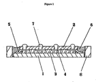
- a semiconductor chip 1 faces a semiconductor chip attachment element 2 (a chip carrier in Figure 1 ) and is bonded thereto by adhesive 3 .
- Interconnects 4 are formed on the surface of the semiconductor chip attachment element 2 that faces the semiconductor chip 1 , and these interconnects 4 and the semiconductor chip 1 are electrically connected by leads 5 .
- a portion or all of the lead 5 is sealed or embedded with a sealant/filling agent 6 .
- the semiconductor attachment element 2 is provided with solder balls 7 .
- an outer frame 8 is provided in order to protect the semiconductor chip 1 from external mechanical stresses, but the nature of this outer frame 8 in semiconductor devices according to the present invention is not critical.
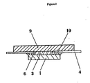
- a semiconductor chip 1 faces a semiconductor chip attachment element 9 (a circuit substrate in Figure 2 ) and is bonded thereto by adhesive 3 .
- Interconnects 4 are formed on the surface of the semiconductor chip attachment element 9 that faces the semiconductor chip 1 , and these interconnects 4 and the semiconductor chip 1 are electrically connected by bumps 10 .
- a portion or all of the bump 10 is sealed or embedded with a sealant/filling agent 6 .
- leads are provided that electrically connect to the interconnects 4 .
- the semiconductor chip 1 may be sealed with a resin sealant.
- the subject semiconductor chip attachment element can be made of for example, a ceramic such as alumina, glass, and the like; an organic resin such as epoxy resin, glass fiber-reinforced epoxy resin, polyimide resin, bismaleimide triazine resin, and the like; and metals such as stainless steel, copper, and the like.
- This element can be, for example, a rigid circuit substrate or chip carrier or a flexible circuit substrate or chip carrier.
- the interconnects can be formed on the surface of or within the semiconductor chip attachment element by such means as printing, vapor deposition, gluing, lamination, plating, and the like.
- connection terminals such as a ball grid of solder balls or a pin grid, and other electrical elements and components may also be mounted or provided.
- Bonding wires, leads, and bumps are examples of the member that electrically connects the semiconductor chip with the interconnects on its semiconductor chip attachment element. In order to relax the stresses acting in this member when the semiconductor device is subjected to thermal stresses, the use is preferred for this member of curved, bent, or flexed bonding wires or leads, or of bumps made of material with a low Young's modulus.
- Either or both of the adhesive bonding the semiconductor chip to its chip attachment element and the sealant/filling agent that seals or embeds the member that electrically connects the semiconductor chip with the interconnects on its chip attachment element must have a complex modulus, measured at -65 °C and a shear frequency of 10 Hz, no greater than 1 ⁇ 10 8 Pa in the semiconductor device according to the present invention.
- the value of this complex modulus is preferably in the range from 1 ⁇ 10 8 Pa to 1 ⁇ 10 2 Pa and more preferably is in the range from 1 ⁇ 10 7 Pa to 1 ⁇ 10 2 Pa.
- the complex modulus of the adhesive and sealant/filling agent at -65 °C and a shear frequency of 10 Hz can be determined by measurement on a strip or disk of the adhesive or sealant/filling agent using a dynamic viscoelastic test instrument.
- the adhesive composition that forms the adhesive under consideration is a silicone adhesive composition.
- the adhesive composition preferably takes the form of a liquid of suitably high viscosity, a grease, or a paste, or a sheet or film made of a B-stage adhesive or a hot-melt adhesive.
- the semiconductor chip can be bonded to its chip attachment element using the subject adhesive composition by, for example, heating the adhesive composition with a hot air current or thermal radiation, bringing the adhesive composition into contact with moist air, or irradiating the adhesive composition with UV radiation or an electron beam.
- the semiconductor chip in the semiconductor device according to the present invention is preferably bonded to the chip attachment element by the adhesive composition through the thermal cure of a thermosetting adhesive composition. Heating the subject adhesive composition forms a cured silicone that is a rubber at ambient temperature.
- the sealant/filling agent composition that forms the sealant/filling agent under discussion is a silicone sealant/filling agent composition.
- the sealant/filling agent composition is preferably a paste or liquid and more preferably is a liquid.
- the member that electrically connects the semiconductor chip with the interconnects on the chip attachment element can be sealed or embedded using the subject sealant/filling agent composition by, for example, heating the sealant/filling agent composition with a hot air current or thermal radiation, bringing the composition into contact with moist air, or irradiating the composition with UV radiation or an electron beam.
- Sealing or embedding with an elastic sealant/filling agent composition is preferably effected in the semiconductor device according to the present invention through the thermal cure of a thermosetting sealant/filling agent composition. Heating the subject sealant/filling agent composition forms a cured silicone that is a rubber at ambient temperature.
- the method for fabricating the semiconductor device according to the present invention is not critical.
- the semiconductor device shown in Figure 1 can be fabricated, for example, by setting up the opposing surfaces of the semiconductor chip 1 and the chip attachment element 2 next to each other with the adhesive composition (high-viscosity liquid, grease, paste, film, or sheet) sandwiched in between; curing the adhesive composition; then electrically connecting the semiconductor chip 1 and the interconnects 4 on the chip attachment element 2 with leads 5 (this connection step may also be carried out prior to curing the adhesive composition); sealing or embedding all or part of the lead 5 with a liquid sealant/filling agent composition; and subsequently curing the sealant/filling agent composition.
- the adhesive composition high-viscosity liquid, grease, paste, film, or sheet
- the semiconductor device shown in Figure 2 can be fabricated by setting up the opposing surfaces of the semiconductor chip 1 and the chip attachment element 9 next to each other with the adhesive composition (high-viscosity liquid, grease, paste, film, or sheet) sandwiched in between; curing the adhesive composition; then electrically connecting the semiconductor chip 1 and the interconnects 4 on the chip attachment element 9 with bumps 10 (this connection step may also be carried out prior to curing the adhesive composition); sealing or embedding all or part of the bump 10 with a liquid sealant/filling agent composition; and subsequently curing the sealant/filling agent composition.
- the adhesive composition high-viscosity liquid, grease, paste, film, or sheet
- the nature of the contact between the subject adhesive and sealant/filling agent in the semiconductor device according to the present invention preferably ranges from bonding per se to acceptably intimate contact.
- the nature of the contact between the sealant/filling agent and the member that electrically connects the semiconductor chip and the interconnects on the chip attachment element preferably also ranges from bonding per se to acceptably intimate contact.
- the adhesive and sealant/filling agent in the semiconductor device according to the present invention can be electrically conductive, semiconductive, or nonconductive, although they are preferably semiconductive or nonconductive, for example, preferably with a volume resistivity at 25 °C of at least 1 ⁇ 10 8 ⁇ cm, when the surface of the semiconductor chip is used facing the chip attachment element.
- thermosetting silicone adhesive composition or thermosetting silicone sealant/filling agent composition at 150 °C for 30 minutes.
- the complex modulus was determined by measurement on this strip using a viscoelastic measurement instrument (a dynamic analyzer from Rheometrics, Inc.).
- each lead 5 was sealed or embedded in its entirety with the thermosetting silicone sealant/filling agent composition, and the sealant/filling agent composition was thereafter cured by heating for 30 minutes at 150 °C.
- each bump 10 was sealed or embedded in its entirety with the thermosetting silicone sealant/filling agent composition, and the sealant/filling agent composition was thereafter cured by heating for 30 minutes at 150 °C.
- the thermal shock resistance of the semiconductor devices fabricated as described above was evaluated as follows.
- thermal shock resistance of the semiconductor devices Twenty semiconductor devices were submitted to thermal shock testing in which 1 cycle consisted of standing for 30 minutes at -65 °C and standing for 30 minutes at +150 °C. The percentage of defective semiconductor devices was determined after 1,000 cycles and 3,000 cycles by continuity testing, using the solder balls 7 on the semiconductor chip attachment element 2 (chip carrier) in the case of semiconductor devices according to Figure 1 and using the interconnects 4 in the case of the semiconductor devices according to Figure 2 .
- the adherence between the adhesive and sealant/filling agent in the semiconductor devices was evaluated as follows.
- the adhesive composition used in this example was a thermosetting silicone adhesive composition grease that formed an adherent silicone rubber upon heating.
- This composition provided a silicone rubber that had a volume resistivity at 25°C of 1.0 ⁇ 10 15 ⁇ cm and a complex modulus of 2.0 ⁇ 10 6 Pa at -65 °C and a shear frequency of 10 Hz.
- the sealant/filling agent composition used to form the sealant/filling agent was a liquid thermosetting silicone sealant/filling agent composition that formed an adherent silicone rubber upon heating.
- This composition provided a silicone rubber that had a volume resistivity at 25 °C of 1.0 ⁇ 10 15 ⁇ cm and a complex modulus of 2.0 ⁇ 10 6 Pa at -65 °C and a shear frequency of 10 Hz.
- This adhesive composition and sealant/filling agent composition were used to fabricate 20 semiconductor devices as shown in Figure 1 . The resulting semiconductor devices were evaluated for thermal shock resistance and for adherence between the adhesive and sealant/filling agent. The results of
- the adhesive composition used in this example was a thermosetting silicone adhesive composition grease that formed an adherent silicone rubber upon heating.
- This composition provided a silicone rubber that had a volume resistivity at 25 °C of 1.0 ⁇ 10 15 ⁇ cm and a complex modulus of 1.5 ⁇ 10 8 Pa at -65 °C and a shear frequency of 10 Hz.
- the sealant/filling agent composition used to form the sealant/filling agent was a liquid thermosetting silicone sealant/filling agent composition that formed an adherent silicone rubber upon heating.
- This composition provided a silicone rubber that had a volume resistivity at 25 °C of 1.0 ⁇ 10 15 ⁇ cm and a complex modulus of 2.0 ⁇ 10 6 Pa at -65 °C and a shear frequency of 10 Hz.
- This adhesive composition and sealant/filling agent composition were used to fabricate 20 semiconductor devices as shown in Figure 1 . The resulting semiconductor devices were evaluated for thermal shock resistance and for adherence between the adhesive and sealant/filling agent. The results
- a sheet of semicured thermosetting silicone adhesive that formed an adherent silicone rubber upon heating was used to form the adhesive in this example.
- the resulting silicone rubber had a volume resistivity at 25 °C of 1.0 ⁇ 10 15 ⁇ cm and a complex modulus of 2.0 ⁇ 10 6 Pa at -65 °C and a shear frequency of 10 Hz.
- the sealant/filling agent composition used to form the sealant/filling agent was a liquid thermosetting silicone sealant/filling agent composition that formed an adherent silicone rubber upon heating.
- This composition provided a silicone rubber that had a volume resistivity at 25 °C of 1.0 ⁇ 10 15 ⁇ cm and a complex modulus of 2.0 ⁇ 10 6 Pa at -65 °C and a shear frequency of 10 Hz.
- This adhesive sheet and sealant/filling agent composition were used to fabricate 20 semiconductor devices as shown in Figure 1 . The resulting semiconductor devices were evaluated for thermal shock resistance and for adherence between the adhesive and sealant/filling agent. The results of
- a sheet of semicured thermosetting silicone adhesive that formed an adherent silicone rubber upon heating was used to form the adhesive in this example.
- the resulting silicone rubber had a volume resistivity at 25 °C of 1.0 ⁇ 10 15 ⁇ cm and a complex modulus of 1.5 ⁇ 10 8 Pa at -65 °C and a shear frequency of 10 Hz.
- the sealant/filling agent composition used to form the sealant/filling agent was a liquid thermosetting silicone sealant/filling agent composition that formed an adherent silicone rubber upon heating.
- This composition provided a silicone rubber that had a volume resistivity at 25 °C of 1.0 ⁇ 10 15 ⁇ cm and a complex modulus of 2.0 ⁇ 10 6 Pa at -65 °C and a shear frequency of 10 Hz.
- This adhesive sheet and sealant/filling agent composition were used to fabricate 20 semiconductor devices as shown in Figure 1 . The resulting semiconductor devices were evaluated for thermal shock resistance and for adherence between the adhesive and sealant/filling agent. The results of
- the adhesive composition used in this example was a thermosetting silicone adhesive composition grease that formed an adherent silicone rubber upon heating.
- This composition provided a silicone rubber that had a volume resistivity at 25 °C of 1.0 ⁇ 10 15 ⁇ cm and a complex modulus of 2.0 ⁇ 10 6 Pa at 65°C and a shear frequency of 10 Hz.
- the sealant/filling agent composition used to form the sealant/filling agent was a liquid thermosetting silicone sealant/filling agent composition that formed an adherent silicone rubber upon heating.
- This composition provided a silicone rubber that had a volume resistivity at 25 °C of 1.0 ⁇ 10 15 ⁇ cm and a complex modulus of 2.0 ⁇ 10 6 Pa at -65 °C and a shear frequency of 10 Hz.
- This adhesive composition and sealant/filling agent composition were used to fabricate 20 semiconductor devices as shown in Figure 2 . The resulting semiconductor devices were evaluated for thermal shock resistance and for adherence between the adhesive and sealant/filling agent. The results of these evaluation
- the adhesive composition used in this example was a thermosetting silicone adhesive composition grease that formed an adherent silicone rubber upon heating.
- This composition provided a silicone rubber that had a volume resistivity at 25°C of 1.0 ⁇ 10 15 ⁇ cm and a complex modulus of 1.5 ⁇ 10 8 Pa at -65 °C and a shear frequency of 10 Hz.
- the sealant/filling agent composition used to form the sealant/filling agent was a liquid thermosetting silicone sealant/filling agent composition that formed an adherent silicone rubber upon heating.
- This composition provided a silicone rubber that had a volume resistivity at 25°C of 1.0 ⁇ 10 15 ⁇ cm and a complex modulus of 2.0 ⁇ 10 6 Pa at -65 °C and a shear frequency of 10 Hz.
- This adhesive composition and sealant/filling agent composition were used to fabricate 20 semiconductor devices as shown in Figure 2 . The resulting semiconductor devices were evaluated for thermal shock resistance and for adherence between the adhesive and sealant/filling agent. The results of these
- a sheet of semicured thermosetting silicone adhesive that formed an adherent silicone rubber upon heating was used to form the adhesive in this example.
- the resulting silicone rubber had a volume resistivity at 25 °C of 1.0 ⁇ 10 15 ⁇ cm and a complex modulus of 2.0 ⁇ 10 6 Pa at -65 °C and a shear frequency of 10 Hz.
- the sealant/filling agent composition used to form the sealant/filling agent was a liquid thermosetting silicone sealant/filling agent composition that formed an adherent silicone rubber upon heating.
- This composition provided a silicone rubber that had a volume resistivity at 25 °C of 1.0 ⁇ 10 15 ⁇ cm and a complex modulus of 2.0 ⁇ 10 6 Pa at -65 °C and a shear frequency of 10 Hz.
- This adhesive sheet and sealant/filling agent composition were used to fabricate 20 semiconductor devices as shown in Figure 2 . The resulting semiconductor devices were evaluated for thermal shock resistance and for adherence between the adhesive and sealant/filling agent. The results of
- a sheet of semicured thermosetting silicone adhesive that formed an adherent silicone rubber upon heating was used to form the adhesive in this example.
- the resulting silicone rubber had a volume resistivity at 25 °C of 1.0 ⁇ 10 15 ⁇ cm and a complex modulus of 1.5 ⁇ 10 8 Pa at -65 °C and a shear frequency of 10 Hz.
- the sealant/filling agent composition used to form the sealant/filling agent was a liquid thermosetting silicone sealant/filling agent composition that formed an adherent silicone rubber upon heating.
- This composition provided a silicone rubber that had a volume resistivity at 25 °C of 1.0 ⁇ 10 15 ⁇ cm and a complex modulus of 2.0 ⁇ 10 6 Pa at -65 °C and a shear frequency of 10 Hz.
- This adhesive sheet and sealant/filling agent composition were used to fabricate 20 semiconductor devices as shown in Figure 2 . The resulting semiconductor devices were evaluated for thermal shock resistance and for adherence between the adhesive and sealant/filling agent. The results of
- a sheet of semicured thermosetting silicone adhesive that formed an adherent silicone rubber upon heating was used to form the adhesive in this comparative example.
- the resulting silicone rubber had a volume resistivity at 25 °C of 1.0 ⁇ 10 15 ⁇ cm and a complex modulus of 1.5 ⁇ 10 8 Pa at -65 °C and a shear frequency of 10 Hz.
- the sealant/filling agent composition used to form the sealant/filling agent was a liquid thermosetting silicone sealant/filling agent composition that formed an adherent silicone rubber upon heating.
- This composition provided a silicone rubber that had a volume resistivity at 25 °C of 1.0 ⁇ 10 15 ⁇ cm and a complex modulus of 1.5 ⁇ 10 8 Pa at -65° C and a shear frequency of 10 Hz.
- This adhesive sheet and sealant/filling agent composition were used to fabricate 20 semiconductor devices as shown in Figure 1 . The resulting semiconductor devices were evaluated for thermal shock resistance and for adherence between the adhesive and sealant/filling agent. The results
- the adhesive composition used in this comparative example was a thermosetting silicone adhesive composition grease that formed an adherent silicone rubber upon heating.
- This composition provided a silicone rubber that had a volume resistivity at 25 °C of 1.0 ⁇ 10 15 ⁇ cm and a complex modulus of 1.5 ⁇ 10 8 Pa at -65 °C and a shear frequency of 10 Hz.
- the sealant/filling agent composition used to form the sealant/filling agent was a liquid thermosetting silicone sealant/filling agent composition that cured upon heating with the formation of a silicone rubber.
- This composition provided a silicone rubber that had a volume resistivity at 25 °C of 1.0 ⁇ 10 15 ⁇ cm and a complex modulus of 1.5 ⁇ 10 8 Pa at -65 °C and a shear frequency of 10 Hz.
- This adhesive composition and sealant/filling agent composition were used to fabricate 20 semiconductor devices as shown in Figure 1 . The resulting semiconductor devices were evaluated for thermal shock resistance and for adherence between the adhesive and sealant/filling agent. The results of these evaluations are reported in Table 1.
- a sheet of semicured thermosetting silicone adhesive that formed an adherent silicone rubber upon heating was used to form the adhesive in this comparative example.
- the resulting silicone rubber had a volume resistivity at 25 °C of 1.0 ⁇ 10 15 ⁇ cm and a complex modulus of 1.5 ⁇ 10 8 Pa at -65 °C and a shear frequency of 10 Hz.
- the sealant/filling agent composition used to form the sealant/filling agent was a liquid thermosetting silicone sealant/filling agent composition that formed an adherent silicone rubber upon heating.
- This composition provided a silicone rubber that had a volume resistivity at 25 °C of 1.0 ⁇ 10 15 ⁇ cm and a complex modulus of 1.5 ⁇ 10 8 Pa at -65 °C and a shear frequency of 10 Hz.
- This adhesive sheet and sealant/filling agent composition were used to fabricate 20 semiconductor devices as shown in Figure 2 . The resulting semiconductor devices were evaluated for thermal shock resistance and for adherence between the adhesive and sealant/filling agent. The results of these evaluations are reported in Table 1.
- the adhesive composition used in this comparative example was a thermosetting silicone adhesive composition grease that formed an adherent silicone rubber upon heating.
- This composition provided a silicone rubber that had a volume resistivity at 25 °C of 1.0 ⁇ 10 15 ⁇ cm and a complex modulus of 1.5 ⁇ 10 8 Pa at -65 °C and a shear frequency of 10 Hz.
- the sealant/filling agent composition used to form the sealant/filling agent was a liquid thermosetting silicone sealant/filling agent composition that formed an adherent silicone rubber upon heating.
- This composition provided a silicone rubber that had a volume resistivity at 25 °C of 1.0 ⁇ 10 15 ⁇ cm and a complex modulus of 1.5 ⁇ 10 8 Pa at -65 °C and a shear frequency of 10 Hz.
- This adhesive composition and sealant/filling agent composition were used to fabricate 20 semiconductor devices as shown in Figure 2 . The resulting semiconductor devices were evaluated for thermal shock resistance and for adherence between the adhesive and sealant/filling agent. The results of these evaluations are reported in Table 1.
- the semiconductor device according to the present invention is characterized by an excellent resistance to thermal shock.
Landscapes
- Structures Or Materials For Encapsulating Or Coating Semiconductor Devices Or Solid State Devices (AREA)
- Wire Bonding (AREA)
- Die Bonding (AREA)
- Encapsulation Of And Coatings For Semiconductor Or Solid State Devices (AREA)
Claims (13)
- Halbleitervorrichtung enthaltend:einen Halbleiterchip (1), ein dem Halbleiterchip (1) gegenüberliegendes Halbleiterchipbefestigungselement (2,9), wenigstens eine Verbindung (4) auf der Oberfläche des Halbleiterchipbefestigungselements (2,9) und wenigstens ein Teil, das den Halbleiterchip (1) mit den Verbindungen (4) elektrisch verbindet, wobei der Halbleiterchip (1) mit dem Halbleiterchipbefestigungselement (2,9) durch einen Klebstoff (3) verbunden ist, der unmittelbar die Oberfläche des Halbleiterchipbefestigungselements (2,9) kontaktiert, und wenigstens einen Teil wenigstens eines Teils, das den Halbleiterchip (1) mit der wenigstens einen Verbindung (4) elektrisch verbindet, mit einem Versiegelungsmittel/Füllmittel (6) versiegelt oder darin eingebettet ist und sowohl der Klebstoff (3) als auch das Versiegelungsmittel/Füllmittel (6) ein gehärteter Siliconkautschuk ist, wobei wenigstens einer von dem Klebstoff (3) und dem Versiegelungsmittel/Füllmittel (6) einen komplexen Modul von nicht größer als 1 x 10⁸ Pa bei -65°C und einer Scherfrequenz von 10 Hz aufweist.
- Halbleitervorrichtung gemäß Anspruch 1, wobei die Halbleitervorrichtung ein integrierter Schaltkreis, ein hochintegrierter Schaltkreis oder ein höchstintegrierter Schaltkreis ist.
- Halbleitervorrichtung gemäß Anspruch 1, wobei das Teil, das den Halbleiterchip (1) mit den Verbindungen (4) verbindet, ein Bonddraht, eine Leitung (5) oder ein Kontakthöcker (10) ist.
- Halblsitervorrichtung gemäß Anspruch 1, wobei der komplexe Modul sowohl des Klebstoffs (3) als auch des Versiegelungsmittels/Füllmittels (6) nicht größer als 1 x 10⁸ Pa bei -65°C und einer Scherfrequenz von 10 Hz ist.
- Halbleitervorrichtung gemäß Anspruch 1, wobei der komplexe Modul von 1 x 10⁸ bis 1 x 10² Pa beträgt.
- Halbleitervorrichtung gemäß Anspruch 5, wobei der komplexe Modul von 1 x 10⁷ bis 1 x 10² Pa beträgt.
- Halbleitervorrichtung gemäß Anspruch 1, wobei der Halbleiterchip (1) an das Halbleiterchipbefestigungselement (2,9) durch Härten einer wärmehärtenden Klebstoffzusammensetzung gebunden ist.
- Halbleitervorrichtung gemäß Anspruch 1, wobei das Teil, das den Halbleiterchip (1) elektrisch mit den Verbindungen (4) verbindet, durch Härten einer wärmehärtenden Versiegelungsmittel/Füllmittelzusammensetzung versiegelt oder darin eingebettet ist.
- Halbleitervorrichtung gemäß Anspruch 1, wobei das Versiegelungsmittel/Füllmittel elektrisch leitfähig, halbleitend oder nichtleitend ist.
- Halbleitervorrichtung gemäß Anspruch 9, wobei das Versiegelungsmittel/Füllmittel (6) halbleitend oder nichtleitend ist.
- Halbleitervorrichtung gemäß Anspruch 10, wobei das Versiegelungsmittel/Füllmittel (6) einen Volumenwiderstand von wenigstens 1 x 10⁸ Ω·cm bei 25°C aufweist.
- Halbleitervorrichtung gemäß Anspruch 1, wobei der Klebstoff (3) elektrisch leitfähig, halbleitend oder nichtleitend ist.
- Halbleitervorrichtung gemäß Anspruch 10, wobei der Klebstoff einen Volumenwiderstand von wenigstens 1 x 10⁸ Ω·cm bei 25°C aufweist.
Applications Claiming Priority (2)
| Application Number | Priority Date | Filing Date | Title |
|---|---|---|---|
| JP21576997A JP3223246B2 (ja) | 1997-07-25 | 1997-07-25 | 半導体装置 |
| JP215769/97 | 1997-07-25 |
Publications (3)
| Publication Number | Publication Date |
|---|---|
| EP0893823A1 EP0893823A1 (de) | 1999-01-27 |
| EP0893823B1 EP0893823B1 (de) | 2012-05-02 |
| EP0893823B9 true EP0893823B9 (de) | 2012-08-08 |
Family
ID=16677929
Family Applications (1)
| Application Number | Title | Priority Date | Filing Date |
|---|---|---|---|
| EP98113868A Expired - Lifetime EP0893823B9 (de) | 1997-07-25 | 1998-07-24 | Struktur zum Bonden und Abdichten eines Halbleiters |
Country Status (2)
| Country | Link |
|---|---|
| EP (1) | EP0893823B9 (de) |
| JP (1) | JP3223246B2 (de) |
Families Citing this family (6)
| Publication number | Priority date | Publication date | Assignee | Title |
|---|---|---|---|---|
| US9892606B2 (en) | 2001-11-15 | 2018-02-13 | Avigilon Fortress Corporation | Video surveillance system employing video primitives |
| US8711217B2 (en) | 2000-10-24 | 2014-04-29 | Objectvideo, Inc. | Video surveillance system employing video primitives |
| US7868912B2 (en) | 2000-10-24 | 2011-01-11 | Objectvideo, Inc. | Video surveillance system employing video primitives |
| JP2005347273A (ja) * | 2005-06-06 | 2005-12-15 | Hitachi Chem Co Ltd | 熱架橋型回路接続材料及びそれを用いた回路板の製造方法 |
| GB201805383D0 (en) | 2018-03-30 | 2018-05-16 | Dow Silicones Corp | Condensation curable compositions |
| GB201805382D0 (en) | 2018-03-30 | 2018-05-16 | Dow Silicones Corp | Condensation curable compositions |
Family Cites Families (6)
| Publication number | Priority date | Publication date | Assignee | Title |
|---|---|---|---|---|
| JPS61230344A (ja) * | 1985-04-05 | 1986-10-14 | Toray Silicone Co Ltd | 樹脂封止型半導体装置 |
| JPH07120733B2 (ja) * | 1985-09-27 | 1995-12-20 | 日本電装株式会社 | 車両用半導体素子パッケージ構造とその製造方法 |
| EP0275588B1 (de) * | 1986-12-19 | 1993-11-10 | Koninklijke Philips Electronics N.V. | Verfahren zum Herstellen einer Halbleitervorrichtung mit vermindertem Verpackungsdruck |
| NL8902018A (nl) * | 1989-08-07 | 1991-03-01 | Philips Nv | Halfgeleiderinrichting. |
| JP2843658B2 (ja) * | 1990-08-02 | 1999-01-06 | 東レ・ダウコーニング・シリコーン株式会社 | フリップチップ型半導体装置 |
| JP2927081B2 (ja) * | 1991-10-30 | 1999-07-28 | 株式会社デンソー | 樹脂封止型半導体装置 |
-
1997
- 1997-07-25 JP JP21576997A patent/JP3223246B2/ja not_active Expired - Fee Related
-
1998
- 1998-07-24 EP EP98113868A patent/EP0893823B9/de not_active Expired - Lifetime
Also Published As
| Publication number | Publication date |
|---|---|
| JPH1145975A (ja) | 1999-02-16 |
| JP3223246B2 (ja) | 2001-10-29 |
| EP0893823A1 (de) | 1999-01-27 |
| EP0893823B1 (de) | 2012-05-02 |
Similar Documents
| Publication | Publication Date | Title |
|---|---|---|
| US6103551A (en) | Semiconductor unit and method for manufacturing the same | |
| EP1174920A2 (de) | Halbleitergehäuse | |
| EP1096565B1 (de) | Harzversiegelte Halbleitervorrichtung und dieselbe enthaltender Flüssigkristallanzeigemodul | |
| EP1448745B1 (de) | Anisotrop elektroleitfaehiger klebefilm, verfahren zu seiner herstellung und halbleitervorrichtungen | |
| EP0340492A2 (de) | Konforme Versieglung und interplanare Verkapselung elektronischer Anordnungsstrukturen | |
| KR100555860B1 (ko) | 접착제 및 밀봉제를 공 경화하여 전자 패키지를 제조하는 방법 | |
| US6621173B1 (en) | Semiconductor device having an adhesive and a sealant | |
| JP2000058589A (ja) | 半導体装置及びその製造方法 | |
| JPH09505444A (ja) | 接着シートを用いたマルチチップ電子パッケージモジュール | |
| US6084306A (en) | Bridging method of interconnects for integrated circuit packages | |
| JP2951102B2 (ja) | 混成集積回路 | |
| EP0469614B1 (de) | Flip-Chip-Halbleiteranordnung | |
| EP0893823B9 (de) | Struktur zum Bonden und Abdichten eines Halbleiters | |
| JP2930186B2 (ja) | 半導体装置の実装方法および半導体装置の実装体 | |
| JP3336240B2 (ja) | 半導体素子実装基板 | |
| JP2786734B2 (ja) | 半導体装置 | |
| JPH05218137A (ja) | 半導体装置の製造方法 | |
| KR900007302B1 (ko) | 반도체 장치 | |
| JPH04171970A (ja) | 半導体装置 | |
| KR100884295B1 (ko) | 반도체 장치의 제조 방법 및 반도체 장치 | |
| Nagai et al. | Anisotropic conductive adhesive films for flip-chip interconnection onto organic substrates | |
| JP3155811B2 (ja) | 樹脂封止型半導体装置の製造方法 | |
| EP0670595B1 (de) | Mit Harz eingekapseltes Halbleiterbauelement | |
| JP2633285B2 (ja) | 車載用混成集積回路装置 | |
| Tanigawa et al. | The resin molded chip size package (MCSP) |
Legal Events
| Date | Code | Title | Description |
|---|---|---|---|
| PUAI | Public reference made under article 153(3) epc to a published international application that has entered the european phase |
Free format text: ORIGINAL CODE: 0009012 |
|
| AK | Designated contracting states |
Kind code of ref document: A1 Designated state(s): DE FR GB IT NL |
|
| AX | Request for extension of the european patent |
Free format text: AL;LT;LV;MK;RO;SI |
|
| 17P | Request for examination filed |
Effective date: 19990505 |
|
| AKX | Designation fees paid |
Free format text: DE FR GB IT NL |
|
| RAP1 | Party data changed (applicant data changed or rights of an application transferred) |
Owner name: DOW CORNING TORAY CO., LTD. |
|
| 17Q | First examination report despatched |
Effective date: 20080222 |
|
| GRAP | Despatch of communication of intention to grant a patent |
Free format text: ORIGINAL CODE: EPIDOSNIGR1 |
|
| GRAS | Grant fee paid |
Free format text: ORIGINAL CODE: EPIDOSNIGR3 |
|
| GRAA | (expected) grant |
Free format text: ORIGINAL CODE: 0009210 |
|
| AK | Designated contracting states |
Kind code of ref document: B1 Designated state(s): DE FR GB IT NL |
|
| REG | Reference to a national code |
Ref country code: GB Ref legal event code: FG4D |
|
| REG | Reference to a national code |
Ref country code: DE Ref legal event code: R096 Ref document number: 69842702 Country of ref document: DE Effective date: 20120628 |
|
| REG | Reference to a national code |
Ref country code: NL Ref legal event code: VDEP Effective date: 20120502 |
|
| RAP2 | Party data changed (patent owner data changed or rights of a patent transferred) |
Owner name: DOW CORNING TORAY CO., LTD. |
|
| PG25 | Lapsed in a contracting state [announced via postgrant information from national office to epo] |
Ref country code: NL Free format text: LAPSE BECAUSE OF FAILURE TO SUBMIT A TRANSLATION OF THE DESCRIPTION OR TO PAY THE FEE WITHIN THE PRESCRIBED TIME-LIMIT Effective date: 20120502 |
|
| PG25 | Lapsed in a contracting state [announced via postgrant information from national office to epo] |
Ref country code: IT Free format text: LAPSE BECAUSE OF FAILURE TO SUBMIT A TRANSLATION OF THE DESCRIPTION OR TO PAY THE FEE WITHIN THE PRESCRIBED TIME-LIMIT Effective date: 20120502 |
|
| PLBE | No opposition filed within time limit |
Free format text: ORIGINAL CODE: 0009261 |
|
| STAA | Information on the status of an ep patent application or granted ep patent |
Free format text: STATUS: NO OPPOSITION FILED WITHIN TIME LIMIT |
|
| 26N | No opposition filed |
Effective date: 20130205 |
|
| GBPC | Gb: european patent ceased through non-payment of renewal fee |
Effective date: 20120802 |
|
| REG | Reference to a national code |
Ref country code: FR Ref legal event code: ST Effective date: 20130329 |
|
| PG25 | Lapsed in a contracting state [announced via postgrant information from national office to epo] |
Ref country code: FR Free format text: LAPSE BECAUSE OF NON-PAYMENT OF DUE FEES Effective date: 20120731 |
|
| REG | Reference to a national code |
Ref country code: DE Ref legal event code: R097 Ref document number: 69842702 Country of ref document: DE Effective date: 20130205 |
|
| PG25 | Lapsed in a contracting state [announced via postgrant information from national office to epo] |
Ref country code: GB Free format text: LAPSE BECAUSE OF NON-PAYMENT OF DUE FEES Effective date: 20120802 |
|
| REG | Reference to a national code |
Ref country code: DE Ref legal event code: R082 Ref document number: 69842702 Country of ref document: DE Representative=s name: FLEISCHER, ENGELS & PARTNER MBB, PATENTANWAELT, DE |
|
| PGFP | Annual fee paid to national office [announced via postgrant information from national office to epo] |
Ref country code: DE Payment date: 20140716 Year of fee payment: 17 |
|
| REG | Reference to a national code |
Ref country code: DE Ref legal event code: R119 Ref document number: 69842702 Country of ref document: DE |
|
| PG25 | Lapsed in a contracting state [announced via postgrant information from national office to epo] |
Ref country code: DE Free format text: LAPSE BECAUSE OF NON-PAYMENT OF DUE FEES Effective date: 20160202 |