EP0893881A2 - Diplexer für Vollduplexkommunikation - Google Patents
Diplexer für Vollduplexkommunikation Download PDFInfo
- Publication number
- EP0893881A2 EP0893881A2 EP98305444A EP98305444A EP0893881A2 EP 0893881 A2 EP0893881 A2 EP 0893881A2 EP 98305444 A EP98305444 A EP 98305444A EP 98305444 A EP98305444 A EP 98305444A EP 0893881 A2 EP0893881 A2 EP 0893881A2
- Authority
- EP
- European Patent Office
- Prior art keywords
- port
- diplexer
- reactive
- network
- splitter
- Prior art date
- Legal status (The legal status is an assumption and is not a legal conclusion. Google has not performed a legal analysis and makes no representation as to the accuracy of the status listed.)
- Withdrawn
Links
- 238000004891 communication Methods 0.000 title description 7
- 230000005540 biological transmission Effects 0.000 claims abstract description 15
- 238000012545 processing Methods 0.000 claims abstract description 4
- 239000013078 crystal Substances 0.000 claims description 6
- 239000010453 quartz Substances 0.000 claims description 3
- VYPSYNLAJGMNEJ-UHFFFAOYSA-N silicon dioxide Inorganic materials O=[Si]=O VYPSYNLAJGMNEJ-UHFFFAOYSA-N 0.000 claims description 3
- 238000002955 isolation Methods 0.000 description 14
- 230000009466 transformation Effects 0.000 description 4
- 238000010586 diagram Methods 0.000 description 3
- 230000000694 effects Effects 0.000 description 3
- 239000003990 capacitor Substances 0.000 description 2
- 230000008859 change Effects 0.000 description 2
- 238000013461 design Methods 0.000 description 2
- 238000003780 insertion Methods 0.000 description 2
- 230000037431 insertion Effects 0.000 description 2
- 238000000034 method Methods 0.000 description 2
- 238000009738 saturating Methods 0.000 description 2
- 238000000844 transformation Methods 0.000 description 2
- 230000002238 attenuated effect Effects 0.000 description 1
- 230000000903 blocking effect Effects 0.000 description 1
- 230000001413 cellular effect Effects 0.000 description 1
- 238000000586 desensitisation Methods 0.000 description 1
- 230000008569 process Effects 0.000 description 1
- 230000009467 reduction Effects 0.000 description 1
- 238000000926 separation method Methods 0.000 description 1
- 230000001131 transforming effect Effects 0.000 description 1
Images


Classifications
-
- H—ELECTRICITY
- H03—ELECTRONIC CIRCUITRY
- H03H—IMPEDANCE NETWORKS, e.g. RESONANT CIRCUITS; RESONATORS
- H03H7/00—Multiple-port networks comprising only passive electrical elements as network components
- H03H7/46—Networks for connecting several sources or loads, working on different frequencies or frequency bands, to a common load or source
Definitions
- This invention relates to a diplexer for full duplex communications.
- diplexer circuits to allow the use of separate frequencies for simultaneous transmission and reception (full duplex operation) on a single antenna or cable is well established.
- Classical diplexer designs employ combinations of low, high and bandpass structures.
- the spacing of the frequencies which can be employed is determined by the nature of the filters employed to construct the diplexer. The closer the frequencies employed, in general, the bigger and more expensive the filters required become if losses, which degrade the quality of the communication, are to be minimised.
- compact bandpass structures can be fabricated using dielectric components. These offer a low loss and they are suitable for the wide frequency separation between the transmitted and received frequencies.
- a diplexer comprising two reactive power splitters and a reactive network.
- a door entry system incorporating a diplexer comprising two reactive power splitters and a reactive network.
- the reactive network can be a series LC network.
- Block 1 is a power splitter combiner. Power applied to a port s is divided between ports a and b . Power delivered to port a is delivered to port s , and power delivered to port b is delivered to port s ; in the ideal case none of the power delivered to port a is delivered to port b , and vice versa
- Block 2 is a receiver mixer.
- the signal which is to be received is applied to port s of the splitter of Block 1 and the fraction of this applied signal delivered to port a is converted by a heterodyne process involving the oscillator frequency produced by an oscillator Block 3 to a frequency suitable for further processing.
- Block 3 is the oscillator, which is a circuit which produces the so-called local oscillator signal for the receiver, and which in this application is used as the transmit frequency.
- Block 4 represents modulator and transmitter stages.
- the information applied to port m is used to modulate a signal delivered to the this stage from the oscillator.
- the output of this stage delivered to port b of the splitter and thence to port s .
- an incoming signal at 27.2 MHz is applied to port s .
- the fraction of the power delivered from port s to port b is lost, and in this context is unimportant.
- the fraction of the power applied to port s and delivered to port a is now applied to the mixer circuit and is mixed with a frequency of 27.4 MHz produced by the oscillator.
- the signal at the mixer output is filtered and further processed to reproduce any information contained by the incoming signal.
- the 27.4 MHz signal produced by the oscillator block is modulated and amplified, and the resultant signal applied to port b of the splitter and thence to port s from which it is launched into the transmitting medium.
- any signal leaking from port b to port a mixes with itself in the mixer and produces a DC signal, which is of no importance to the system.
- the leaking signal desensitises the mixer by either saturating its input, saturating its output, or the DC signal produced upsets the mixer bias. In any of these cases the result is the same, the system performance degrades.
- the splitter can be a soldered joint if care is taken to maintain the impedance levels; this however introduces no isolation between ports a and b.
- a more sophisticated splitter employs a resistor network, but the isolation obtained between ports a and b is also reflected as a loss introduced between the sum port s and ports a and b ; this can only reduce the system performance. Such systems cannot therefore be regarded as true diplexer circuits.
- the system performance can be restored to its optimum if the isolation between ports a and b can be increased, without introducing additional loss between port a and port s .
- Suitable frequency selective components can be introduced which will reject the unwanted signals at each port, but which must be large if losses are to be minimised.
- transformer based power splitters can solve the above problems. Such devices are commercially available from Mini-Circuits.
- the equivalent circuit of the transformer based power splitter is shown in Figure 2.
- Minimum insertion loss from port s to ports a and b will occur when port s is terminated in a value of zo/2; R has a value of 2zo and ports a and b are terminated in zo. Under these conditions, power applied to port s will be equally divided between ports a and b (i.e. 1/2 the power to each). However power applied to port a ( b ) will not be delivered to port b ( a ). Interestingly, if ports a and b are not terminated in zo, whilst the insertion loss from port s to port a or b will be detrimentally affected, the isolation between ports a and b is hardly affected.
- Figure 3 shows how the isolation between ports a and b varies with the termination resistance at port s .
- FIG. 4 shows a splitter used as a diplexer with port s terminated in an antenna.
- a relatively broad band impedance extending from 27.2 MHz to 27.4 MHz would be required.
- a perfect diplexer is formed if port s is correctly terminated.
- port s can be terminated in an antenna designed to have a purely resistive component of z0/2 at the transmission frequency, providing a large isolation between ports a and b at the transmission frequency, whilst delivering transmitter power to the sum port s from port a , and received power from the sum port s to port a .
- the isolation obtained between ports a and b by relying on the impedance of the antenna is not reliable, because the impedance presented by the antenna to the sum port s is highly dependant upon the environment into which the antenna is placed.
- the impedance is known and unlikely to vary; however, in a hand held environment the antenna environment can change as the hand held unit is moved relatively to the body of the user and the impedance can change, whereby output can drop dramatically.
- a method of ensuring that the isolation obtained does not fall below an acceptable minimum can be realised by employing the properties of the splitter and series LC circuits (a tuned or resonant circuit).
- the impedance of a series tuned LC network falls to the dynamic resistance of an inductor, the effect of a finite capacitance Q is negligible due to the very high Q of the capacitor.
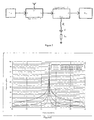
- Figure 5 shows the impedance of a 3 ⁇ H inductor having a Q of 100 and a 12pF capacitor. The impedance falls close to 5 ⁇ as expected from the Q value. Note that the impedance is only purely resistive at the frequency producing this minimum resistance (the resonant frequency). Placing an additional 20 ⁇ in series with this network will give a pure resistance of 25 ⁇ when the circuit comes to resonance.
- Figure 6 shows the isolations obtained with purely resistive and reactive sum port s terminations as functions of frequency.
- An attenuation notch is produced by the use of the series resonant LC circuit.
- the invention envisages the use of two splitters and a reactive network to produce a diplexing circuit with deep notch characteristics which acts as a stable filter of unwanted noise.
- the diplexer can be used in a door entry system such as a door 'phone system. As described above, available systems tend to rely on a simple summing junction, and by using the transmit frequency as the local oscillator produces a DC level at the mixer output, which is considered insignificant.
- the diplexer according to the invention uses two reactive power splitters and a series LC network.
- the antenna can in theory provide the correct impedance to the sum port of a reactive splitter to provide the required isolation in a system as shown in Figure 4.
- changing environments mean that the antenna impedance cannot be relied upon and the isolation of the splitter cannot be guaranteed to be adequate.
- Figure 7 shows how two splitters and a reactive network can be used to produce a diplexer which is independent of the antenna environment.
- Splitter 1 performs the basic splitting/combining function.
- the power from the transmitter at port a is coupled to the antenna at port S1; clearly if the antenna impedance is correct, considerable attenuation of the transmitter power occurs between ports a and b .
- Received power is coupled from the antenna at S1 to port b .
- the required attenuation of the transmitter power coupled to port c on splitter 2 due to the non optimal termination of the port S1 by the antenna, is performed by the notch produced by the reactive network on port S2. By placing the peak attenuation over the transmitted frequency, the transmitter power is attenuated between ports c and d . However, at the receive frequency the termination of port S2 is not ideal and little attenuation of the received signal occurs.
- the reactive network on S2 is constructed in such a manner that it is unaffected by its local environment. Thus, if when ideally terminated at the sum port an isolation of ndB is produced, this will always be the minimum attenuation produced by this new two splitter diplex circuit. Additional attenuation will be obtained as the match on S1 improves; the theoretical maximum attenuation is 2n dB.
- the notch shown in Figure 6 is produced by a network represented on port S2 as a series LC circuit.
- the series LC network can however be realised in a number of ways, in particular a crystal could be employed to produce a highly stable very narrow notch.
- Other reactive networks connected to port S2 produce other transmission characteristics between ports c and d .
- optimum termination impedance of the summing port controls the notch width.
- the narrower the notch the closer the transmitter and receiver frequencies can be.
- the notch shown in Figure 6 is obtained when the ideal termination impedance is zo/2.
- the intrinsic zo/2 impedance at the sum port can be transformed to required value.
- the effect of transforming the sum port impedance to both higher and lower impedance's than zo/2 is shown in Figure 8.
- the required impedance transformation can be achieved in a number of ways.
- the classic Ruthroff and Guanella transmission line transformers provide simple means of achieving impedance transformations of 3:1, 4:1, multiples thereof and some non integer impedance transformations; whilst the so called ROTRA transmission line configuration provides non integer transformation matching networks. These transformers are wideband structures and maintain the intrinsically wide bandwidth of the transformer based diplexer.
- a quartz crystal which can be represented as having an equivalent circuit consisting of a series LCR network, will provide a much narrower notch.
- Figure 9 shows the notch produced for a 27MHz crystal having a Q of 9500.
- Parallel resonant networks can also be employed.
Landscapes
- Transceivers (AREA)
Applications Claiming Priority (2)
| Application Number | Priority Date | Filing Date | Title |
|---|---|---|---|
| GB9715486 | 1997-07-22 | ||
| GB9715486A GB2328346A (en) | 1997-07-22 | 1997-07-22 | Diplexer for full duplex communications |
Publications (2)
| Publication Number | Publication Date |
|---|---|
| EP0893881A2 true EP0893881A2 (de) | 1999-01-27 |
| EP0893881A3 EP0893881A3 (de) | 2002-11-13 |
Family
ID=10816295
Family Applications (1)
| Application Number | Title | Priority Date | Filing Date |
|---|---|---|---|
| EP98305444A Withdrawn EP0893881A3 (de) | 1997-07-22 | 1998-07-08 | Diplexer für Vollduplexkommunikation |
Country Status (2)
| Country | Link |
|---|---|
| EP (1) | EP0893881A3 (de) |
| GB (1) | GB2328346A (de) |
Cited By (1)
| Publication number | Priority date | Publication date | Assignee | Title |
|---|---|---|---|---|
| KR20020093281A (ko) * | 2001-06-07 | 2002-12-16 | 엘지전자 주식회사 | 이중밴드 통신 단말기의 다이플렉서 회로 |
Families Citing this family (1)
| Publication number | Priority date | Publication date | Assignee | Title |
|---|---|---|---|---|
| US7635270B2 (en) | 2006-05-31 | 2009-12-22 | At&T Intellectual Property I, L.P. | Method and apparatus for transferring digital packet-based data |
Family Cites Families (6)
| Publication number | Priority date | Publication date | Assignee | Title |
|---|---|---|---|---|
| US3656162A (en) * | 1969-09-19 | 1972-04-11 | Litton Systems Inc | Diplexer for radio communication |
| US4080601A (en) * | 1976-04-01 | 1978-03-21 | Wacom Products, Incorporated | Radio frequency filter network having bandpass and bandreject characteristics |
| US4240155A (en) * | 1978-06-28 | 1980-12-16 | Micro Communications, Inc. | Diplexer and multiplexer |
| US4210881A (en) * | 1978-11-09 | 1980-07-01 | The United States Of America As Represented By The Secretary Of The Navy | Millimeter wave microstrip triplexer |
| US5180999A (en) * | 1990-09-28 | 1993-01-19 | Rockwell International Corporation | Filter system with controlled amplitude in stopband or passband |
| GB2297459A (en) * | 1995-01-26 | 1996-07-31 | Airtech Ltd | A mast head device |
-
1997
- 1997-07-22 GB GB9715486A patent/GB2328346A/en not_active Withdrawn
-
1998
- 1998-07-08 EP EP98305444A patent/EP0893881A3/de not_active Withdrawn
Cited By (1)
| Publication number | Priority date | Publication date | Assignee | Title |
|---|---|---|---|---|
| KR20020093281A (ko) * | 2001-06-07 | 2002-12-16 | 엘지전자 주식회사 | 이중밴드 통신 단말기의 다이플렉서 회로 |
Also Published As
| Publication number | Publication date |
|---|---|
| GB2328346A (en) | 1999-02-17 |
| GB9715486D0 (en) | 1997-10-01 |
| EP0893881A3 (de) | 2002-11-13 |
Similar Documents
| Publication | Publication Date | Title |
|---|---|---|
| US4910481A (en) | Branching filter | |
| EP0441500B1 (de) | Funksende-Empfänger | |
| KR100437627B1 (ko) | 전력 증폭기용 임피던스 정합 회로 | |
| US5640686A (en) | Radio communication device capable of communication in a plurality of communication systems | |
| US4973940A (en) | Optimum impedance system for coupling transceiver to power line carrier network | |
| US5815804A (en) | Dual-band filter network | |
| US7339445B2 (en) | BAW duplexer without phase shifter | |
| US6603372B1 (en) | Laminated notch filter and cellular phone using the same | |
| US10069479B1 (en) | Tunable filter for RF circuits | |
| JPH07307655A (ja) | 送受信分離装置 | |
| WO1990005388A1 (en) | Ceramic filter having integral phase shifting network | |
| CA1198782A (en) | Miniaturized antenna duplexer using saw filter | |
| US4612571A (en) | Constant Z bandswitched input filter | |
| US6738604B2 (en) | Programmable IF bandwidth using fixed bandwidth filters | |
| US6983129B2 (en) | Radio frequency switch and wireless communication apparatus using the same | |
| US7403082B2 (en) | Dual mode antenna switch module | |
| US5721521A (en) | Notch-enhancement in band-reject filters | |
| US4691379A (en) | Mixer circuit | |
| EP0893881A2 (de) | Diplexer für Vollduplexkommunikation | |
| EP1999855A1 (de) | Empfänger, sender und empfangsverfahren | |
| US20040251958A1 (en) | Active filter | |
| JP2004200853A (ja) | 高周波回路装置 | |
| JPH09232909A (ja) | 分波器 | |
| JP3398243B2 (ja) | アンテナ共用器 | |
| KR100906776B1 (ko) | 스위치 lna가 구비된 iss 필터 모듈 |
Legal Events
| Date | Code | Title | Description |
|---|---|---|---|
| PUAI | Public reference made under article 153(3) epc to a published international application that has entered the european phase |
Free format text: ORIGINAL CODE: 0009012 |
|
| AK | Designated contracting states |
Kind code of ref document: A2 Designated state(s): AT BE CH CY DE DK ES FI FR GB GR IE IT LI LU MC NL PT SE |
|
| AX | Request for extension of the european patent |
Free format text: AL;LT;LV;MK;RO;SI |
|
| PUAL | Search report despatched |
Free format text: ORIGINAL CODE: 0009013 |
|
| AK | Designated contracting states |
Kind code of ref document: A3 Designated state(s): AT BE CH CY DE DK ES FI FR GB GR IE IT LI LU MC NL PT SE |
|
| AX | Request for extension of the european patent |
Free format text: AL;LT;LV;MK;RO;SI |
|
| 17P | Request for examination filed |
Effective date: 20030506 |
|
| AKX | Designation fees paid |
Designated state(s): DE FR GB |
|
| STAA | Information on the status of an ep patent application or granted ep patent |
Free format text: STATUS: THE APPLICATION HAS BEEN WITHDRAWN |
|
| 18W | Application withdrawn |
Effective date: 20040719 |