EP0895371A2 - Interface à multiplexage dans le temps entre un dispositif central et des dispositifs décentraux - Google Patents
Interface à multiplexage dans le temps entre un dispositif central et des dispositifs décentraux Download PDFInfo
- Publication number
- EP0895371A2 EP0895371A2 EP98111347A EP98111347A EP0895371A2 EP 0895371 A2 EP0895371 A2 EP 0895371A2 EP 98111347 A EP98111347 A EP 98111347A EP 98111347 A EP98111347 A EP 98111347A EP 0895371 A2 EP0895371 A2 EP 0895371A2
- Authority
- EP
- European Patent Office
- Prior art keywords
- pbg1
- zbg1
- time
- information
- transmission
- Prior art date
- Legal status (The legal status is an assumption and is not a legal conclusion. Google has not performed a legal analysis and makes no representation as to the accuracy of the status listed.)
- Granted
Links
Images


Classifications
-
- H—ELECTRICITY
- H04—ELECTRIC COMMUNICATION TECHNIQUE
- H04Q—SELECTING
- H04Q11/00—Selecting arrangements for multiplex systems
- H04Q11/04—Selecting arrangements for multiplex systems for time-division multiplexing
- H04Q11/0421—Circuit arrangements therefor
-
- H—ELECTRICITY
- H04—ELECTRIC COMMUNICATION TECHNIQUE
- H04J—MULTIPLEX COMMUNICATION
- H04J3/00—Time-division multiplex systems
- H04J3/02—Details
- H04J3/06—Synchronising arrangements
- H04J3/0602—Systems characterised by the synchronising information used
- H04J3/0605—Special codes used as synchronising signal
- H04J3/0608—Detectors therefor, e.g. correlators, state machines
-
- H—ELECTRICITY
- H04—ELECTRIC COMMUNICATION TECHNIQUE
- H04J—MULTIPLEX COMMUNICATION
- H04J3/00—Time-division multiplex systems
- H04J3/02—Details
- H04J3/12—Arrangements providing for calling or supervisory signals
-
- H—ELECTRICITY
- H04—ELECTRIC COMMUNICATION TECHNIQUE
- H04J—MULTIPLEX COMMUNICATION
- H04J3/00—Time-division multiplex systems
- H04J3/02—Details
- H04J3/14—Monitoring arrangements
-
- H—ELECTRICITY
- H04—ELECTRIC COMMUNICATION TECHNIQUE
- H04Q—SELECTING
- H04Q11/00—Selecting arrangements for multiplex systems
- H04Q11/04—Selecting arrangements for multiplex systems for time-division multiplexing
-
- H—ELECTRICITY
- H04—ELECTRIC COMMUNICATION TECHNIQUE
- H04Q—SELECTING
- H04Q3/00—Selecting arrangements
- H04Q3/58—Arrangements providing connection between main exchange and sub-exchange or satellite
-
- H—ELECTRICITY
- H04—ELECTRIC COMMUNICATION TECHNIQUE
- H04Q—SELECTING
- H04Q2213/00—Indexing scheme relating to selecting arrangements in general and for multiplex systems
- H04Q2213/1302—Relay switches
-
- H—ELECTRICITY
- H04—ELECTRIC COMMUNICATION TECHNIQUE
- H04Q—SELECTING
- H04Q2213/00—Indexing scheme relating to selecting arrangements in general and for multiplex systems
- H04Q2213/13031—Pulse code modulation, PCM
-
- H—ELECTRICITY
- H04—ELECTRIC COMMUNICATION TECHNIQUE
- H04Q—SELECTING
- H04Q2213/00—Indexing scheme relating to selecting arrangements in general and for multiplex systems
- H04Q2213/1304—Coordinate switches, crossbar, 4/2 with relays, coupling field
-
- H—ELECTRICITY
- H04—ELECTRIC COMMUNICATION TECHNIQUE
- H04Q—SELECTING
- H04Q2213/00—Indexing scheme relating to selecting arrangements in general and for multiplex systems
- H04Q2213/1305—Software aspects
-
- H—ELECTRICITY
- H04—ELECTRIC COMMUNICATION TECHNIQUE
- H04Q—SELECTING
- H04Q2213/00—Indexing scheme relating to selecting arrangements in general and for multiplex systems
- H04Q2213/13166—Fault prevention
-
- H—ELECTRICITY
- H04—ELECTRIC COMMUNICATION TECHNIQUE
- H04Q—SELECTING
- H04Q2213/00—Indexing scheme relating to selecting arrangements in general and for multiplex systems
- H04Q2213/13167—Redundant apparatus
-
- H—ELECTRICITY
- H04—ELECTRIC COMMUNICATION TECHNIQUE
- H04Q—SELECTING
- H04Q2213/00—Indexing scheme relating to selecting arrangements in general and for multiplex systems
- H04Q2213/13174—Data transmission, file transfer
-
- H—ELECTRICITY
- H04—ELECTRIC COMMUNICATION TECHNIQUE
- H04Q—SELECTING
- H04Q2213/00—Indexing scheme relating to selecting arrangements in general and for multiplex systems
- H04Q2213/13176—Common channel signaling, CCS7
-
- H—ELECTRICITY
- H04—ELECTRIC COMMUNICATION TECHNIQUE
- H04Q—SELECTING
- H04Q2213/00—Indexing scheme relating to selecting arrangements in general and for multiplex systems
- H04Q2213/13178—Control signals
-
- H—ELECTRICITY
- H04—ELECTRIC COMMUNICATION TECHNIQUE
- H04Q—SELECTING
- H04Q2213/00—Indexing scheme relating to selecting arrangements in general and for multiplex systems
- H04Q2213/13202—Network termination [NT]
-
- H—ELECTRICITY
- H04—ELECTRIC COMMUNICATION TECHNIQUE
- H04Q—SELECTING
- H04Q2213/00—Indexing scheme relating to selecting arrangements in general and for multiplex systems
- H04Q2213/13213—Counting, timing circuits
-
- H—ELECTRICITY
- H04—ELECTRIC COMMUNICATION TECHNIQUE
- H04Q—SELECTING
- H04Q2213/00—Indexing scheme relating to selecting arrangements in general and for multiplex systems
- H04Q2213/13215—Code checking, CRC
-
- H—ELECTRICITY
- H04—ELECTRIC COMMUNICATION TECHNIQUE
- H04Q—SELECTING
- H04Q2213/00—Indexing scheme relating to selecting arrangements in general and for multiplex systems
- H04Q2213/13216—Code signals, frame structure
-
- H—ELECTRICITY
- H04—ELECTRIC COMMUNICATION TECHNIQUE
- H04Q—SELECTING
- H04Q2213/00—Indexing scheme relating to selecting arrangements in general and for multiplex systems
- H04Q2213/1322—PBX
-
- H—ELECTRICITY
- H04—ELECTRIC COMMUNICATION TECHNIQUE
- H04Q—SELECTING
- H04Q2213/00—Indexing scheme relating to selecting arrangements in general and for multiplex systems
- H04Q2213/13292—Time division multiplexing, TDM
-
- H—ELECTRICITY
- H04—ELECTRIC COMMUNICATION TECHNIQUE
- H04Q—SELECTING
- H04Q2213/00—Indexing scheme relating to selecting arrangements in general and for multiplex systems
- H04Q2213/1336—Synchronisation
Definitions
- time division multiplex oriented communication facilities for example in facilities of feeder networks or in Communication systems are between their central and decentralized Components time-multiplex oriented communication interfaces realized.
- a well-known time division multiplex oriented The PCM 30 - Interface that exists between the switching matrix and the peripheral Subscriber connection facilities of a communication system is arranged.
- Another time division oriented Interface represents the from the publication 'ISDN in the office, Hicom', Siemens AG, 1986, p.58 to 66 well-known PCM highway interface through 4 x 32 PCM transmission channels is formed. Signaling channels not via the PCM highway, but separately via the switching technology Establishments in communication systems.
- the object underlying the invention is to be seen in a universal interface between central and decentralized components of communication devices to design.
- the task is characterized by the characteristics of claim 1 solved.
- time-division-oriented Interface The essential aspect of the time-division-oriented Interface can be seen in the fact that several in Time slots arranged for transmission frames for serial Transmission of user information, mediation Information, safety and operational information, Programs in the sense of loading components of the Communication device and frame clock and / or superframe clock information are provided.
- An advantage of the invention time-division-oriented interface to be seen in the fact that no additional connections between the central and decentralized components of communication facilities required for a communication exchange are. This means that development is largely independent of central and decentralized components of communication facilities - For example, central switching networks and peripheral connection assemblies of communication systems - Is possible, the connections between the components are reduced to a minimum.
- Another advantage of the invention time-division-oriented interface to see that the individual information, such as safety, operational and switching technology Information transmitted in separate time slots and thus a simultaneous, undisturbed transmission of information between the components is made possible.
- a time slot through data bits is advantageous, at least a signaling bit and at least one parity bit are formed - Claim 2.
- at least one additional signaling bit can in addition to the actual data bits - for example digitized voice information - additional channel-oriented signaling information - i.e. Signaling information to the respective connection - simultaneously or additionally transmitted.
- the signaling bit is in central signaling concepts for the Transmission channels - for example a central signaling channel with the V.5 interface - not required, i.e. the signaling bit is used if necessary.
- the at least one parity bit increases the security of the data transmission.
- processor-oriented processing advantageously eight data bits, one signaling bit and one Parity bit provided per time slot - claim 3.
- the useful information to be transmitted in the data bits NZR-coded and odd parity bits formed and from the received user information and parity bits becomes the bit clock for the bit-wise processing of the received information derived - claim 4.
- NZR coding and use of an odd parity bit is achieved in each transmitted time slot.
- an edge change of the received Data signal is generated.
- clock signals indicating the bit clock become. These clock signals are called system clock signals to the subsequent units or components of the respective Communication device for bit processing of the information received.
- the time-division-oriented Interface advantageously a time slot for the transmission of switching information, two time slots for the transmission of safety and operational technology Information, four time slots for loading of programs, 154 timeslots for the transmission of time-multiplex-oriented useful information and a time slot for the transmission of frame clock and / or frame clock information on - claim 5.
- the respective transmission capacity i.e. the number of time slots on the required transmission capacities regarding the individual information groups Voted.
- the time-division-oriented interface is physical advantageously bidirectional with symmetrical 2-wire information transmission realized - claim 6.
- Advantageous line drivers and receivers can be used in a known 3.3 V or 5 V technology can be used.
- the interface is the two time slots for the transmission of safety and operational technology Information for redundant components of the communication device provided - claim 7.
- These will be advantageous two time slots for the transmission of security and operational information in a communication arrangement with central and decentral components with each time-division-oriented interfaces.
- Every decentralized component is bidirectional with every central one Component via time-division-oriented interfaces connected, with each decentralized component a time slot for the transmission of safety and operational technology Information is associated.
- the central and decentralized Components are means of recognizing the failure provided, with a failure of central components safety-related information indicating the failure the assigned time slot for the transmission of safety and operational information to the with it connected decentralized components is transmitted.
- the decentralized components are interconnected means to switch to the redundant component in the case a failure of a central or decentralized component provided - claim 8.
- the respective components are in the receiving direction actively operated and one of the two components as active component defined and if one component fails is only by the corresponding switch or switch active participation of the failed component blocked or excluded.
- the redundancy circuit is advantageously implemented the in the direction of transmission to the decentralized Component acting time-division-oriented interfaces by a switch and in the direction of transmission central component acting time-division-oriented Interfaces using a switch - claim 9.
- FIG 1 shows a continuous, time slot-oriented Information flow is that over a time division oriented Interface ISI - in FIG 1 by the parenthesized Designation ISI indicated - between central and decentralized Components of a transmission device transmitted becomes.
- the parenthesized Designation ISI indicated - between central and decentralized Components of a transmission device transmitted becomes.
- bidirectional time-division-oriented interfaces ISI is in either direction such information flow is communicable.
- the continuous flow of information is similar structured transmission frame FR structured.
- Any transmission frame FR are assigned 162 time slots ZS1..ZS162.
- the transmission frames FR at a speed of 8 kHz (125 ⁇ s) be transmitted.
- Such a frequency is particular for the transmission of digitized voice information suitable with a sampling rate of 8 kHz.
- the transmission frame FR are the first 154 time slots ZS1..ZS154 for the Transmission of user information ni - for example digitized Voice information or other data - provided.
- the four other time slots namely the 155th to 158th Time slots ZS155..ZS158 are for loading programs PR intended.
- these time slots ZS155..ZS158 for example from a central component - for example a microprocessor system with program memory - the respective Application programs PR to the decentralized or peripheral Components - such as a line connector assembly of a communication system - during commissioning the peripheral or decentralized components or assemblies loaded.
- This loading of PR programs can also be done during the Operation of the time-multiplex-oriented interface ISI, for example, an updated application program PR in the peripheral or decentralized component too save and put into operation.
- Time slot ZS159 is for the transmission of switching technology Information provided cp, in this Time slot ZS159 in particular as part of the signaling between a communication system and a communication terminal provided signaling information for the time slots ZS1..154 for the transmission of user information not transmitted in packets.
- signaling information or switching technology Information cp for analog or digital communication terminals transmitted.
- safety and operational information sbi transmitted.
- Safety and operational information sbi provide in particular operational instructions for operation that Administration and maintenance of the respective central or decentralized components.
- Component-related error or operating status messages transmitted via the two time slots ZS160, ZS161.
- special bit patterns so-called Frame synchronization bit pattern or synchronous words transfer.
- this synchronization bit pattern in the receiving component of the information stream Frame rate determined in a known manner.
- this Frame clock With the help of this Frame clock becomes the beginning or the end of a transmission frame FR determined and then the individual Time slots ZS1..ZS162 scanned and processed accordingly.
- ZS162 is in the last time slot if necessary, a bit for the display of an overframe clock signal ürt defined. This means that if the bit is set, the frame clock signal specified in this transmission frame FR rt simultaneously represents the superframe clock signal.
- a time slot ZS generally comprises 10 bits, with 8 bits D1..8 for the Transmission of user information ni, a bit for the transmission of additional information cas and a parity bit P are provided.
- the number of 8 bits D1..8 is one Transmission of digitized voice information with one Width of 8 bits, i.e. on PCM transmission of voice information Voted.
- the bit for the transmission of additional Information cas are, for example, the useful bits ni associated signaling information cas transmitted.
- the signaling information cas is the respective voice channel - determined by the 8 useful bits D1..8 - assigned signaling information - in the professional world referred to as chanel associated signaling - transmitted.
- the bit for the transmission of additional information cas can be used as needed, i.e. when using central signaling concepts or signaling channels For example, this bit remains unused or is used for the transmission of further transmission channel-specific Information used.
- FIG. 2 also shows the structure of the 162nd time slot ZS162 shown.
- ZS162 is the first Bit R reserved for the identification of a superframe.
- 8 bits in which the frame sync word is entered - in FIG 2 is an example of a synchronization word 11100110 registered.
- the frame synchronization words SW and the first bit R for the Identification of an overframe is also a 10th bit Parity bit P provided.
- time slots ZS1 shown in FIG. 2. .ZS162 and the structure of a transmission frame shown in FIG 1 FR results in a data transmission speed of 12.96 megabits / sec. about the time division oriented ISI interface.
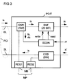
- FIG. 3 shows in a block diagram an implementation of a bidirectional, multiplex-oriented interface ISI in an interface unit PCIT.
- Receive lines EL the multiplex-oriented interface ISI are on a synchronization unit DSR conducted in which received from the serial information stream is the clock signal ts and the frame clock signal rts is derived.
- the frame clock signal rts is done by recognizing and decoding the frame sync word SW recovered in the 162nd time slot ts.
- the recovery of the clock signal is done by the NZR coding and the use of an odd parity bit the user information reached ni, so in each transmitted time slot an edge change of the received Data signal is generated. With at least one edge change can synchronize a phase locked loop at the receiving end in which clock signals ts be generated.
- These clock signals ts are called system clock signals to the subsequent units or components of the respective Communication device for bit processing of the information received.
- the received serial information stream is then in 20 bit wide elastic buffer BUF continuously registered.
- the write-in signal write is in a synchronization unit SCON from the transmitted clock signal ts or frame clock signal rt derived.
- the BUF buffer stores the information stream bit by bit with the help of one formed in the synchronization unit SCON Read signals read out bit by bit and as an information stream is to further components, not shown or units forwarded.
- For system clock-compliant Readout or for forming the readout signal is read the synchronization unit SCON the clock IT supplied.
- An over the multiplex-oriented interface PCI to send out information stream is' is in the interface unit PCIT a coding unit COD supplied in which the synchronization word SW is inserted in the 162nd time slot ZS162.
- the transmission frame FR according to an internal supplied transmission clock transmitted to the transmission line SL.
- the in the synchronization unit DSR and the coding unit COD Synchronization words SW can be used with these Units DSR, COD connected first and second registers REG1, REG2 can be specified.
- the two registers REG1, REG2 are via a microprocessor bus MB, not shown, with a Microprocessor MP connected. From this the respective Synchronization words SW are loaded into the registers REG1, REG2.
- FIG. 4 shows a block diagram of two central components or central assemblies ZBG1, ZBG1 ', to the example two peripheral components or peripheral assemblies PBG1, PBG1 'are connected.
- Several are usually peripheral Assemblies - not shown - on two, for example redundant central modules connected.
- the central ones and peripheral modules (PBG1, PBG1 ', ZBG1, ZBG1') are in one Communication device - by a dashed line Rectangle indicated - for example an optical network unit arranged.
- PBG1, PBG1 ', ZBG1, ZBG1' are in one Communication device - by a dashed line Rectangle indicated - for example an optical network unit arranged.
- these are in the direction of transmission from the respective assembly BG outgoing lines of the respective Interface ISI with A .. and the incoming lines the respective interface ISI with E ..
- a second input E2, E2 'of the peripheral and redundant peripheral assembly PBG1, PBG1 ' is respectively with a third output A3, A3 'of the central or redundant central assembly ZBG1, ZBG1 'connected.
- the first and second output A1 ', A2' of the peripheral redundant module PBG1 ' is on a first input E1' of the redundant central assembly ZBG 'or to a first input E1 of central module ZBG1 switched.
- the third exit A3 ' the redundant central module ZBG1 ' is also open a third input E3 of the peripheral assembly PBG1.
- the third exit A3 is the central one Module ZBG1 additionally on the third input E3 'of redundant peripheral module PBG1 'out.
- time-division-oriented interfaces ISI contained time slots ZS160, 161 can the respective operational or safety information sbi for the respective switching processes or for the Display of the failure of the respective central or decentralized Module PBG1, PBG1 ', ZBG1, ZBG1' are transmitted.
- the time-division-oriented interface according to the invention ISI can be found in any communication device in central and decentralized components or redundant central and decentralized components are structured, usable, where at the receiving and transmitting connection points one time-division-oriented interface each ISI is provided.
Landscapes
- Engineering & Computer Science (AREA)
- Computer Networks & Wireless Communication (AREA)
- Signal Processing (AREA)
- Physics & Mathematics (AREA)
- Astronomy & Astrophysics (AREA)
- General Physics & Mathematics (AREA)
- Time-Division Multiplex Systems (AREA)
- Optical Communication System (AREA)
- Use Of Switch Circuits For Exchanges And Methods Of Control Of Multiplex Exchanges (AREA)
Applications Claiming Priority (2)
| Application Number | Priority Date | Filing Date | Title |
|---|---|---|---|
| DE19733164A DE19733164B4 (de) | 1997-07-31 | 1997-07-31 | Zeitmultiplexorientierte Schnittstelle zwischen zentralen und dezentralen Komponenten von Kommunikationsanordnungen |
| DE19733164 | 1997-07-31 |
Publications (3)
| Publication Number | Publication Date |
|---|---|
| EP0895371A2 true EP0895371A2 (fr) | 1999-02-03 |
| EP0895371A3 EP0895371A3 (fr) | 2005-10-12 |
| EP0895371B1 EP0895371B1 (fr) | 2008-08-13 |
Family
ID=7837595
Family Applications (1)
| Application Number | Title | Priority Date | Filing Date |
|---|---|---|---|
| EP98111347A Expired - Lifetime EP0895371B1 (fr) | 1997-07-31 | 1998-06-19 | Interface à multiplexage dans le temps entre un dispositif central et des dispositifs décentraux |
Country Status (3)
| Country | Link |
|---|---|
| EP (1) | EP0895371B1 (fr) |
| AT (1) | ATE405045T1 (fr) |
| DE (2) | DE19733164B4 (fr) |
Cited By (2)
| Publication number | Priority date | Publication date | Assignee | Title |
|---|---|---|---|---|
| WO2001045453A1 (fr) * | 1999-12-17 | 2001-06-21 | Siemens Aktiengesellschaft | Reseau de couplage non bloquant |
| WO2001045366A3 (fr) * | 1999-12-17 | 2001-12-27 | Siemens Ag | Interface de transmission de donnees pour un reseau de commutation et procede de test correspondant |
Family Cites Families (6)
| Publication number | Priority date | Publication date | Assignee | Title |
|---|---|---|---|---|
| IT1071840B (it) * | 1976-11-12 | 1985-04-10 | Olivetti & Co Spa | Sistema multiprocessore per la commutazione automatica di linee telegrafiche e metodo di trasferimento dei caratteri di informazione |
| GB2151884B (en) * | 1983-12-16 | 1987-05-13 | Standard Telephones Cables Ltd | Timing extraction |
| US5151896A (en) * | 1990-09-21 | 1992-09-29 | Bowman Donald J | Modular digital telephone system with fully distributed local switching and control |
| JP2558012B2 (ja) * | 1990-11-27 | 1996-11-27 | 富士通株式会社 | 通信回線バックアップ方式 |
| JP2722879B2 (ja) * | 1991-08-22 | 1998-03-09 | 日本電気株式会社 | 予備切替方式 |
| US5812951A (en) * | 1994-11-23 | 1998-09-22 | Hughes Electronics Corporation | Wireless personal communication system |
-
1997
- 1997-07-31 DE DE19733164A patent/DE19733164B4/de not_active Expired - Fee Related
-
1998
- 1998-06-19 DE DE59814266T patent/DE59814266D1/de not_active Expired - Fee Related
- 1998-06-19 AT AT98111347T patent/ATE405045T1/de not_active IP Right Cessation
- 1998-06-19 EP EP98111347A patent/EP0895371B1/fr not_active Expired - Lifetime
Cited By (2)
| Publication number | Priority date | Publication date | Assignee | Title |
|---|---|---|---|---|
| WO2001045453A1 (fr) * | 1999-12-17 | 2001-06-21 | Siemens Aktiengesellschaft | Reseau de couplage non bloquant |
| WO2001045366A3 (fr) * | 1999-12-17 | 2001-12-27 | Siemens Ag | Interface de transmission de donnees pour un reseau de commutation et procede de test correspondant |
Also Published As
| Publication number | Publication date |
|---|---|
| EP0895371A3 (fr) | 2005-10-12 |
| EP0895371B1 (fr) | 2008-08-13 |
| ATE405045T1 (de) | 2008-08-15 |
| DE59814266D1 (de) | 2008-09-25 |
| DE19733164A1 (de) | 1999-02-18 |
| DE19733164B4 (de) | 2006-11-02 |
Similar Documents
| Publication | Publication Date | Title |
|---|---|---|
| DE69513643T2 (de) | Fernmeldevermittlungsanlage mit verbesserter redundanz | |
| DE2848255C2 (fr) | ||
| EP0360924B1 (fr) | Procédé de contrôle de centraux de télécommunications à division dans le temps commandés par horloge, en particulier des centraux téléphoniques MIC avec des réseaux de commutation distribués, connectés à un réseau de commutation central | |
| EP0690635B1 (fr) | Procédé de chargement de programmes dans des systèmes de communication avec des équipements décentralisés et non-redundants | |
| EP0765050A2 (fr) | Méthode pour contrÔler la transmission de signaux numériques de communication par un support de transmission à multiplexage temporel | |
| EP0895371B1 (fr) | Interface à multiplexage dans le temps entre un dispositif central et des dispositifs décentraux | |
| DE4207675C1 (fr) | ||
| EP0209946A2 (fr) | Dispositifs de génération d'un marquage de voies de transmission non utilisées d'un système de transmission numérique | |
| DE2718317A1 (de) | Digital koppelnde fernmeldevermittlungseinrichtung | |
| EP0185936B1 (fr) | Montage de circuit d'interface pour la connexion de sources de données avec récepteurs de données et systèmes de commutation avec de tels montages de circuit d'interface | |
| EP0459005B1 (fr) | Méthode et arrangement de transmission d'information de l'état de fonctionnement entre les dispositifs centraux et décentralisés d'un système de communication | |
| EP0530393A1 (fr) | Méthode et dispositif pour la synchronisation d'un générateur d'horloge d'un système de commutation de communication | |
| EP1133197A1 (fr) | Dispositif de commutation | |
| EP0751692B1 (fr) | Procédé pour la connexion de réseaux d'accès avec interfaces V5.2 à des systèmes de communication pourvus de dispositifs périphériques non-redondants | |
| EP0195478B1 (fr) | Méthode et circuit pour la commutation sans sauts de phase de signaux numériques à large bande dans un réseau synchrone de communication à large bande | |
| DE3932700C2 (de) | Verfahren zur Durchschalteprüfung eines Koppelnetzes | |
| EP0475135A1 (fr) | Système de transmission pour réseau de connection dans des reseaux de communication | |
| DE19618953C2 (de) | Synchroner Taktschaltkreis | |
| DE4122276A1 (de) | Digitales kommunikationssystem | |
| EP0974215A2 (fr) | Liaison de communication de donnees dans un reseau de communication hierarchique a bus, fonctionnant selon un protocole demande/reponse, a savoir selon le "protocole d'appel selectif" | |
| DE3212236C1 (de) | Schaltungsanordnung für zentralgesteuerte Fernmeldeanlagen, insbesondere Fernsprechnebenstellenanlagen, mit über Datenübertragungsleitungsbündel steuerbaren zentralen und dezentralen Einrichtungen (zentrale Fehlererkennungseinrichtungen) | |
| DE69025757T2 (de) | Busarchitektur für Kommunikationssystem | |
| EP0263563B1 (fr) | Central à multiplexage temporel | |
| DE3843182C2 (fr) | ||
| DE3037419C2 (de) | Schaltungsanordnung zum Überwachen unzulässiger Verbindungen in einem Koppelfeld für Vermittlungsanlagen, insbesondere Fernsprechvermittlungsanlagen |
Legal Events
| Date | Code | Title | Description |
|---|---|---|---|
| PUAI | Public reference made under article 153(3) epc to a published international application that has entered the european phase |
Free format text: ORIGINAL CODE: 0009012 |
|
| AK | Designated contracting states |
Kind code of ref document: A2 Designated state(s): AT BE CH CY DE DK ES FI FR GB GR IE IT LI LU MC NL PT SE |
|
| AX | Request for extension of the european patent |
Free format text: AL;LT;LV;MK;RO;SI |
|
| PUAL | Search report despatched |
Free format text: ORIGINAL CODE: 0009013 |
|
| AK | Designated contracting states |
Kind code of ref document: A3 Designated state(s): AT BE CH CY DE DK ES FI FR GB GR IE IT LI LU MC NL PT SE |
|
| AX | Request for extension of the european patent |
Extension state: AL LT LV MK RO SI |
|
| 17P | Request for examination filed |
Effective date: 20060411 |
|
| AKX | Designation fees paid |
Designated state(s): AT CH DE FR GB IT LI NL SE |
|
| 17Q | First examination report despatched |
Effective date: 20060821 |
|
| RAP1 | Party data changed (applicant data changed or rights of an application transferred) |
Owner name: NOKIA SIEMENS NETWORKS GMBH & CO. KG |
|
| RAP3 | Party data changed (applicant data changed or rights of an application transferred) |
Owner name: NOKIA SIEMENS NETWORKS S.P.A. |
|
| RAP3 | Party data changed (applicant data changed or rights of an application transferred) |
Owner name: NOKIA SIEMENS NETWORKS GMBH & CO. KG |
|
| GRAP | Despatch of communication of intention to grant a patent |
Free format text: ORIGINAL CODE: EPIDOSNIGR1 |
|
| GRAS | Grant fee paid |
Free format text: ORIGINAL CODE: EPIDOSNIGR3 |
|
| GRAA | (expected) grant |
Free format text: ORIGINAL CODE: 0009210 |
|
| AK | Designated contracting states |
Kind code of ref document: B1 Designated state(s): AT CH DE FR GB IT LI NL SE |
|
| REG | Reference to a national code |
Ref country code: GB Ref legal event code: FG4D Free format text: NOT ENGLISH |
|
| REG | Reference to a national code |
Ref country code: CH Ref legal event code: EP |
|
| REF | Corresponds to: |
Ref document number: 59814266 Country of ref document: DE Date of ref document: 20080925 Kind code of ref document: P |
|
| REG | Reference to a national code |
Ref country code: CH Ref legal event code: NV Representative=s name: SIEMENS SCHWEIZ AG |
|
| REG | Reference to a national code |
Ref country code: SE Ref legal event code: TRGR |
|
| REG | Reference to a national code |
Ref country code: CH Ref legal event code: PCAR Free format text: SIEMENS SCHWEIZ AG;INTELLECTUAL PROPERTY FREILAGERSTRASSE 40;8047 ZUERICH (CH) |
|
| PLBE | No opposition filed within time limit |
Free format text: ORIGINAL CODE: 0009261 |
|
| STAA | Information on the status of an ep patent application or granted ep patent |
Free format text: STATUS: NO OPPOSITION FILED WITHIN TIME LIMIT |
|
| 26N | No opposition filed |
Effective date: 20090514 |
|
| REG | Reference to a national code |
Ref country code: CH Ref legal event code: PL |
|
| GBPC | Gb: european patent ceased through non-payment of renewal fee |
Effective date: 20090619 |
|
| NLV4 | Nl: lapsed or anulled due to non-payment of the annual fee |
Effective date: 20100101 |
|
| REG | Reference to a national code |
Ref country code: FR Ref legal event code: ST Effective date: 20100226 |
|
| PG25 | Lapsed in a contracting state [announced via postgrant information from national office to epo] |
Ref country code: LI Free format text: LAPSE BECAUSE OF NON-PAYMENT OF DUE FEES Effective date: 20090630 Ref country code: FR Free format text: LAPSE BECAUSE OF NON-PAYMENT OF DUE FEES Effective date: 20090630 Ref country code: CH Free format text: LAPSE BECAUSE OF NON-PAYMENT OF DUE FEES Effective date: 20090630 |
|
| PG25 | Lapsed in a contracting state [announced via postgrant information from national office to epo] |
Ref country code: GB Free format text: LAPSE BECAUSE OF NON-PAYMENT OF DUE FEES Effective date: 20090619 |
|
| PG25 | Lapsed in a contracting state [announced via postgrant information from national office to epo] |
Ref country code: DE Free format text: LAPSE BECAUSE OF NON-PAYMENT OF DUE FEES Effective date: 20100101 |
|
| PG25 | Lapsed in a contracting state [announced via postgrant information from national office to epo] |
Ref country code: NL Free format text: LAPSE BECAUSE OF NON-PAYMENT OF DUE FEES Effective date: 20100101 |
|
| PG25 | Lapsed in a contracting state [announced via postgrant information from national office to epo] |
Ref country code: AT Free format text: LAPSE BECAUSE OF NON-PAYMENT OF DUE FEES Effective date: 20090619 |
|
| PG25 | Lapsed in a contracting state [announced via postgrant information from national office to epo] |
Ref country code: IT Free format text: LAPSE BECAUSE OF NON-PAYMENT OF DUE FEES Effective date: 20090619 |
|
| PG25 | Lapsed in a contracting state [announced via postgrant information from national office to epo] |
Ref country code: SE Free format text: LAPSE BECAUSE OF NON-PAYMENT OF DUE FEES Effective date: 20090620 |