EP0896432B1 - Synchrone Verzögerungsschaltung - Google Patents
Synchrone Verzögerungsschaltung Download PDFInfo
- Publication number
- EP0896432B1 EP0896432B1 EP98109781A EP98109781A EP0896432B1 EP 0896432 B1 EP0896432 B1 EP 0896432B1 EP 98109781 A EP98109781 A EP 98109781A EP 98109781 A EP98109781 A EP 98109781A EP 0896432 B1 EP0896432 B1 EP 0896432B1
- Authority
- EP
- European Patent Office
- Prior art keywords
- delay circuit
- clock
- chain
- delay
- output
- Prior art date
- Legal status (The legal status is an assumption and is not a legal conclusion. Google has not performed a legal analysis and makes no representation as to the accuracy of the status listed.)
- Expired - Lifetime
Links
- 230000001360 synchronised effect Effects 0.000 title claims description 59
- 238000005259 measurement Methods 0.000 claims description 31
- 239000004065 semiconductor Substances 0.000 claims description 19
- 230000000295 complement effect Effects 0.000 claims description 12
- 230000015572 biosynthetic process Effects 0.000 claims description 10
- 238000003786 synthesis reaction Methods 0.000 claims description 10
- 230000001902 propagating effect Effects 0.000 claims description 6
- 230000000644 propagated effect Effects 0.000 claims description 5
- 238000012544 monitoring process Methods 0.000 claims description 4
- 230000000630 rising effect Effects 0.000 claims description 4
- 230000002194 synthesizing effect Effects 0.000 claims description 4
- 238000010586 diagram Methods 0.000 description 21
- 238000000034 method Methods 0.000 description 18
- 238000013461 design Methods 0.000 description 13
- 230000004913 activation Effects 0.000 description 5
- 230000001419 dependent effect Effects 0.000 description 5
- 230000008569 process Effects 0.000 description 5
- 230000006870 function Effects 0.000 description 4
- 230000012447 hatching Effects 0.000 description 4
- 238000012546 transfer Methods 0.000 description 4
- 238000010276 construction Methods 0.000 description 3
- 230000001934 delay Effects 0.000 description 2
- 230000008030 elimination Effects 0.000 description 2
- 238000003379 elimination reaction Methods 0.000 description 2
- 238000012986 modification Methods 0.000 description 2
- 230000004048 modification Effects 0.000 description 2
- 241001640034 Heteropterys Species 0.000 description 1
- 102100037224 Noncompact myelin-associated protein Human genes 0.000 description 1
- 101710184695 Noncompact myelin-associated protein Proteins 0.000 description 1
- 230000008859 change Effects 0.000 description 1
- 230000003247 decreasing effect Effects 0.000 description 1
- 238000012938 design process Methods 0.000 description 1
- 238000011161 development Methods 0.000 description 1
- 230000018109 developmental process Effects 0.000 description 1
- 230000000694 effects Effects 0.000 description 1
- 238000012163 sequencing technique Methods 0.000 description 1
- 239000002699 waste material Substances 0.000 description 1
Images












Classifications
-
- H—ELECTRICITY
- H03—ELECTRONIC CIRCUITRY
- H03K—PULSE TECHNIQUE
- H03K5/00—Manipulating of pulses not covered by one of the other main groups of this subclass
- H03K5/13—Arrangements having a single output and transforming input signals into pulses delivered at desired time intervals
- H03K5/133—Arrangements having a single output and transforming input signals into pulses delivered at desired time intervals using a chain of active delay devices
-
- H—ELECTRICITY
- H03—ELECTRONIC CIRCUITRY
- H03K—PULSE TECHNIQUE
- H03K5/00—Manipulating of pulses not covered by one of the other main groups of this subclass
- H03K5/13—Arrangements having a single output and transforming input signals into pulses delivered at desired time intervals
- H03K5/135—Arrangements having a single output and transforming input signals into pulses delivered at desired time intervals by the use of time reference signals, e.g. clock signals
Definitions
- This invention relates to a semiconductor integrated circuit and, more particularly, to a synchronous delay circuit for controlling a clock signal.
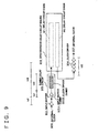
- a synchronous delay circuit basically comprises a delay circuit 901 used to measure a fixed time difference, a delay circuit 902 for reconstructing the measured delay time, and a dummy delay circuit 905 having a delay time corresponding to delay times td1 + td2 obtained by adding delay times td1, td2 of an input buffer 903 and clock driver 904.
- the dummy delay circuit 905 is composed of an input buffer dummy 905A, which uses circuitry exactly the same as that of the input buffer, and a clock driver dummy 905B.
- the delay circuits 901 and 902 are constituted by delay circuit chains having equal delay times and for this reason are also referred to as delay circuit chains.
- the purpose of the delay circuits 901 and 902 is to measure a fixed period of time (this is the function of circuit 901) and reconstruct this period of time (this is the function of circuit 902). This purpose can be attained by causing a signal to advance through the delay circuit 901 and arrange it so that a number of delay elements equal to the number of delay elements through which the signal passed in the delay circuit 901 will be traversed by the signal in the delay circuit 902.
- Methods of arranging it so that a number of delay elements equal to the number of delay elements through which the signal passed in the delay circuit 901 will be traversed by the signal in the delay circuit 902 can be divided into two categories depending upon the propagation directions of the delay circuits 901 and 902 and into two categories depending upon whether the end is selected or the overall path in order to decide the length of the delay circuit 902. There are four types in each of the two categories.
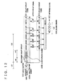
- Figs. 12 and 13 the propagation directions of the delay circuits 901 and 902 are the same and length is decided on the output terminal side of the delay circuit 902 in order to decide the number of elements in the delay circuit 902
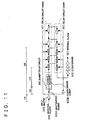
- Figs. 10 and 11 the propagation directions of the delay circuits 901 and 902 are opposite each other and length is decided on the input terminal side of the delay circuit 902 in order to decide the number of elements in the delay circuit 902.
- Fig. 10 corresponds to the scheme described in the above-mentioned Japanese Patent Application Laid-Open No. 8-237091 field by the present inventor which document corresponds to EP-A-0720291 and forms the basis of the preamble of claim 1.
- Fig. 11 corresponds to the scheme described in the above-mentioned literature (4) (IEICE TRANS. ELECTRON., VOL. E79-C, No. 6, June, 1996, pp. 798 ⁇ 807).
- Fig. 12 corresponds to the scheme described in the above-mentioned literature (2) (1996 Symp. on VLSI Circ., pp. 192 ⁇ 193).
- Fig. 13 corresponds to the scheme described in the above-mentioned literature (3) (Proc. of IEEE 1992 CICC 25.2) and in the above-mentioned literature (2) (1996 Symp. on VLSI Circ., pp. 112 ⁇ 113).
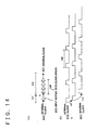
- Fig. 14 illustrates a case in which a synchronous delay circuit is not used.
- an external clock 906 is utilized as an internal clock 907 supplied to the internal circuitry of a semiconductor integrated circuit device through the input buffer 903 and the clock driver 904.
- the delay time between the external clock 906 and the internal clock 907 is decided by the delay time td1 of the input buffer 903 and the delay time td2 of the clock driver 904.
- the sum td1 + td2 is clock skew.
- the timing of the internal clock output by the clock driver becomes equal to the timing of the external clock.
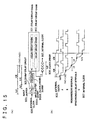
- Fig. 15(b) shows a timing chart for a case in which a synchronous delay circuit is actually used.
- the first period is used to measure the delay time tCK - (td1 + td2) dependent upon the clock period and to decide the delay length of the delay circuit that reconstructs the delay tCK - (td1 + td2).
- the next period is used for the amount of delay of tCK - (td1 + td2).
- the dummy delay circuit 905 of the clock driver 904 and the delay circuit chain 901 are used to measure the delay time tCK - (td1 + td2) dependent upon the clock period.
- the output of input buffer 903 resulting from the first pulse of two consecutive pulses of external clock 906 is caused to advance through dummy delay circuit 905 and delay circuit 901 in one clock period tCK, which extends up to output of the second pulse from the input buffer 903. Since the delay time of the dummy delay circuit 905 is td1 + td2, the time needed for a pulse to advance through the delay circuit 901 is tCK - (td1 + td2).
- the delay time of the delay circuit 902 is set to be equal to the time tCK - (td1 + td2) that was required for the pulse to advance through the delay circuit 901.
- a clock pulse that has been output by the input buffer 903 passes through the delay circuit 902 whose delay is tCK - (td1 + td2) and is output by the clock driver 904 to thereby produce the internal clock 907 whose delay is exactly equal to the clock cycle tCK.
- the process described above provides the internal clock 907, which is free of clock skew, in two clock periods.
- the circuit for doubling the clock frequency ( frequency doubling circuit) and for generating Duty50 is made up of paired delay circuits, namely a delay circuit for measuring a pre-set time difference and a delay circuit for reproducing the delay time, and is configured for doubling the delay time of the delay circuit for reproducing the delay time to a speed twice as high as that of the delay circuit for measuring the pre-set time difference.
- the circuit for doubling the clock frequency and for generating Duty50 is frequently used in combination with the skew eliminating circuit.
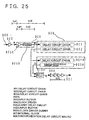
- Fig.25 shows an example of a basic configuration of a synchronous delay circuit.
- this conventional synchronous delay circuit is a conventional synchronous delay circuit, explained with reference to Fig.9, to which are annexed a pair of delay circuit chain. That is, the synchronous delay circuit shown in Fig.25 further comprises a pair of delay circuit chains, made up of a delay circuit chain 901 for measuring the clock period, and a delay circuit chain 902 for reproducing the measured delay time, and a pair of delay circuit chains, made up of a delay circuit chain 901A for measuring the pre-set time difference and a delay circuit chain 902A for reproducing the measured delay time (speed-doubling delay circuit chain), with the two pairs of the delay circuit chains being connected in series with each other.
- An output of the delay circuit chain 902 and an output of the speed-doubling delay circuit chain 902A are synthesized by a synthesis circuit 910A so as to be supplied to a clock driver 904 with delay time td2.
- This double frequency generating and Duty50 generating circuit may be classified similarly to the skew removing circuit.
- the synchronous delay circuit utilizes the properties of the clock pulses being entered every clock period tCK. That is, a delay circuit chain (902A of Fig.25) with a delay time of tCK/2 is provided and the delay time with respect to the pre-input clock is set so as to be equal to one-half the clock period tCK. The clock signals so set are then synthesized with the original clock signals (output C of the delay circuit chain 902 of Fig.25) to provide the double frequency (E of Fig.25) or Duty50%.
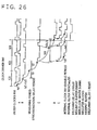
- Fig.26 shows a timing chart representing the waveform of each node of Fig.25.
- the operation of the synchronous delay circuit for double frequency generation and Duty50 generation is in need of 1.5 periods.
- the first one period is used for measuring the delay time tCK which depends on the clock period and for determining the delay length of the delay time adapted for reproducing the delay amount of tCK/2.
- the next period is used for the delay amount of tCK/2.
- a delay circuit chain 901A In measuring the clock-period-dependent delay time tCK for the first period, a delay circuit chain 901A is used. An output of the first pulse delay circuit chain 902 for the first one of two consecutive pulses of the clocks 906 (C of Figs.25 and 26) proceeds through the delay circuit chain 901A during one clock period tCK until outputting of the second delay circuit chain 902. That is, the time during which the pulse proceeds through the delay circuit chain 901A represents the clock period tCK.
- the delay time of the delay circuit chain 902A is set so as to be equal to one-half tCK which is the time during which the pulse proceeded through the delay circuit chain 901A.
- the methods for setting the delay time of the delay circuit chain 902A are roughly classified into four according to desired objectives to be achieved.
- the clocks exiting the delay circuit chain 901A are output through the delay circuit chain 902A having the delay quantity equal to tCK/2 (signal D of Figs.25 and 26) so as to be synthesized with the clock exiting the delay circuit chain 902 (signal C of Figs.25 and 26) and output to generate internal clocks 907 of the double frequency and internal clocks of the Duty50 (907A of Fig.26).
- this conventional synchronous delay circuit execute clock skew removal and frequency doubling- Duty50 with two clock periods and with 1.5 periods, respectively, thus requiring 3.5 clocks (3.5 tCK) as the time required for skew removal.
- a transistor gate process for designing the dummy delay circuit and a wiring process which governs the actual clock delay represent separate design processes.
- designing the clock dummy delay circuit is difficult and it is necessary to design the dummy delay circuit after the wiring is laid out. This is highly inefficient.
- the pattern designed in advance as a macro is solely that of the delay circuit chains 901, 902, and it is necessary to acquire an area for the clock driver dummy 905B beforehand (see Fig. 9) for purposes of layout. This is uneconomical.
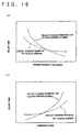
- the delay quantity of the clock driver dummy and that of the original clock driver produce difference in the temperature and source voltage dependency of the delay time, as shown in Fig.16, such that it is difficult to realize satisfactory matching of characteristics.
- an object of the present invention is to provide a synchronous delay circuit that dispenses with a clock driver dummy delay circuit, wherein even if the circuit is applied to a device such as an ASIC in which the amount of clock delay differs from chip to chip, it is no longer necessary to design a clock driver dummy whenever a wiring design is changed and no longer necessary to give consideration to the layout of an area for the clock driver dummy, thereby making possible highly efficient, economical design.
- a synchronous delay circuit comprising a first delay circuit chain propagating a pulse or pulse edge therethrough for a fixed period of time, a second delay circuit chain capable of passing a pulse or pulse edge over a length proportional to the length of the first delay circuit chain along which the pulse or pulse edge propagated, and a circuit outputting a monitor signal for a period of time over which a clock pulse is propagating through a clock driver, wherein the first delay circuit chain is constituted by a clocked inverter and propagation of the pulse or pulse edge through the first delay circuit chain is halted at any desired timing during the output of the monitor signal.
- the synchronous delay circuit includes a first delay circuit chain for allowing pulses or pulse edges to proceed for a pre-set time, a second delay circuit chain allowing pulses or pulse edges to travel therethrough a length proportionate to the length by which the pulses or pulse edges travel through the first delay circuit chain, and a circuit for retrieving monitoring signals during the period the clock pulses are traveling through the clock driver, the first delay circuit chain being formed by a clocked inverter and travel of the pulses or edges through the first delay circuit chain being halted at any desired timing during outputting of the monitoring signals.
- the synchronous delay circuit according to a third aspect of the present invention also includes a third delay circuit chain for allowing pulses or pulse edges to proceed for a pre-set time, and a second delay circuit chain allowing pulses or pulse edges to travel therethrough a length proportionate to the length by which the pulses or pulse edges travel through a fourth delay circuit chain, the third delay circuit chain being formed by a clocked inverter, with the clocks being halted during any desired period of time after allowing the pulses or pulse edges to travel through the fourth delay circuit chain for a pre-set period.
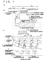
- Fig.1 shows a constitution of a synchronous delay circuit according to a first embodiment of the present invention and a timing chart.
- the first embodiment of the present invention includes a synchronous delay circuit made up of a delay circuit chain 1 for measuring a pre-set time interval, a delay circuit chain 2 for reproducing the measured delay time, the input buffer 3 and the clock driver 4.
- the clock driver 4 furnishes internal clocks 7 to an internal circuit (sequencing circuit), not shown.
- An input dummy 5 is configured similarly to the input buffer 4 and has the same delay time.
- An output A of the input buffer 3 is sent to an input end of a switch 10 (changeover unit) and to the delay circuit chain 1 for measuring the period. To the other input end of the switch 10 is entered an output of the delay circuit chain 2 for reproducing the delay.
- An output of the switch 10 is sent to an input of the clock driver 4 and to a reset terminal of a monitor signal generating circuit 9.
- An output of the clock driver 4 is supplied via the input dummy 5 to a set terminal of the monitor signal generating circuit 9, an output D of which is sent to the delay circuit chain 1.
- the monitor signal generating circuit 9 outputs the monitor signal D, by way of activation thereof, during the time clock pulses are traveling through the clock driver 4 and the input dummy 5.
- the clock period is measured by allowing the clock signals to pass through the delay circuit chain 1 used for measurement.
- the monitor signal D from the monitor signal generating circuit 9 becomes active to inhibit signal passage through the delay circuit chain 1 to discontinue the measurement of the clock period tCK.
- a monitor signal generating circuit 9 for outputting a monitor signal D in the period of time during which a pulse is propagating through the clock driver 4 and input buffer dummy 5 is constituted by an RS flip-flop or the like.
- the monitor signal generating circuit 9 outputs the monitor signal D for a period of time equivalent to this excess time, namely for a period of time equivalent to the remainder obtained by dividing the sum of the delays of clock driver 4 and input buffer dummy 5 by the clock period tCK.
- the monitor signal D halts the signal undergoing measurement in the delay circuit chain 1. Consequently, clock skew is eliminated even in a case where the sum of the delays of clock driver 4 and input buffer dummy 5 is longer than the clock period tCK.
- the monitor signal D that halts the propagation of the clock signal through the delay circuit chain 1 monitors the period of time over which the clock pulse traverses the clock driver 4. This means that the timing at which the clock pulse propagates through the clock driver 4 becomes earlier by tCK - (td1 + td2) from the moment the clock has been synchronized. Accordingly, at the changeover from the state before synchronization to the state after synchronization, the monitor signal D will output two times in one period. (This is indicated by the shaded signal portion of the monitor signal D and the signal portion preceding it in the timing chart of Fig. 1(c).) However, this is avoided by halting the shaded monitor signal D in the timing chart of Fig.
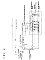
- Fig. 2 is a diagram showing a circuit arrangement according to a first example of the present invention.
- This example employs a scheme in which a delay circuit chain 11 for measuring the clock period tCK and a delay circuit chain 12 for reconstructing the measured period are arranged in mutually opposing directions.
- This scheme in which the delay circuit chain 11 and the delay circuit chain 12 for reconstructing the measured period are arranged in opposite directions is such that a clock pulse propagates through the delay circuit chain 11 and then is transferred to the delay circuit chain 12 via a control circuit chain 18 when the next clock pulse is output by an input buffer 13.
- This arrangement corresponds to the scheme set forth in Japanese Patent Application Laid-Open No. 8-137091 described above in connection with Fig. 10.
- the arrangement shown in Fig. 2 comprises the delay circuit chain 11 capable of extracting an output from any position along the signal transfer path, the delay circuit chain 12 capable of accepting a signal from any position along the signal transfer path, and a control circuit chain 18 having signal input terminals, signal output terminals and input/output control terminals.
- the delay circuit chains 11 and 12 are so arranged that their signal transfer paths are in opposing directions. Sides near the input to the delay circuit chain 11 and sides near the output of the delay circuit chain 12 are successively connected via the control circuit chain 18. After a signal enters the delay circuit chain 11, a signal enters an input/output control terminal of the control circuit chain 18 and a signal in the delay circuit chain 11 is transferred to the delay circuit chain 12.
- Fig. 3 is a diagram showing the construction of the delay circuit chain 11, delay circuit chain 12 and control circuit 18 according to this embodiment.
- this example of the present invention is so adapted that the elements constituting the delay circuit 11 and delay circuit 12 construct clocked inverters.
- N-channel MOS transistors MN11, MN12 and P-channel MOS transistors MP11, MP12 are turned off by a signal D generated by a monitor signal generating circuit (SR flip-flop) 19 from the input and output of the clock driver 14, whereby the clock pulse is not allowed to propagate through the delay circuit chain 11.
- SR flip-flop monitor signal generating circuit
- the RS flip-flop 19 is set, as a result of which the signal D rises to the high level.
- the signal D is at the low level and the MOS transistors are OFF.
- the clocked inverter of the delay circuit 12 is arranged to provide a delay time equal to that of the delay circuit 11 and is ON at all times. That is, the design is such that MOS transistors MN13, MN14, MP13, MP14 are in the ON state.
- An nth delay element will be described with reference to Fig. 3.
- An output FIn of an (n-1)th inverter (not shown) of the delay circuit chain 11 enters a NAND gate 11 and is connected to whichever input terminal of two input terminals of a NAND gate of the control circuit chain 18 is not connected to a control terminal A.
- An output MNn of the NAND gate of control circuit 18 is connected to whichever input terminal of two input terminals of an (n+1)th NAND gate (not shown) of the delay circuit chain 11 is not connected to the output FIn+1 of an nth inverter INV12, and is further connected to whichever input terminal of two input terminals of a NAND gate 14 in the delay circuit chain 12 is not connected to an output BIn+1 of the preceding inverter.
- the output of the NAND gate 14 of delay circuit chain 12 is connected to the input of an inverter INV13 of the delay circuit chain 12.
- the output BIn+1 of the preceding inverter of NAND gate 14 of delay circuit chain 12 enters the NAND gate 14 and is connected to whichever input terminal of two input terminals of a NAND gate 15 (a load adjusting element) is not connected to a ground line.
- the output of the NAND gate 15 constituting the ground adjusting element is left unconnected (i.e., the output is left in the open state).
- the input buffer dummy 15 is placed in front of the delay circuit chain 11, in a manner similar to that of the prior art.
- the time for passage of a signal is equal to that of the input buffer 3.
- the time required for a clock pulse to travel through the delay circuit chain 11 can be made tCK - (td1 + td2) in the manner described above.
- Circuits and wiring such as for the clock driver 14 and input buffer 13 which differ depending upon the ASIC chip cannot be laid out in a macro.
- the clock driver 14, input buffer 13 and input buffer dummy 15 are disposed externally of a synchronous delay circuit macro 20.
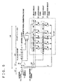
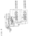
- Fig. 6 is a diagram illustrating a circuit arrangement according to a second example of the present invention.
- this example employs a scheme in which the delay circuit chain 11 for measuring the clock period tCK and the delay circuit chain 12 for reconstructing the measured period are arranged in the same direction.
- This scheme in which the delay circuit chain 11 and the delay circuit chain 12 for reconstructing the measured period are arranged in the same direction is such that a clock pulse propagates through the delay circuit chain 11 and the output of the delay circuit chain 12 is selected when the next clock pulse is output by the input buffer 13.
- This arrangement corresponds to the scheme set forth in literature (2) (1996 Symp. on VLSI Circ. pp. 192 ⁇ 193), explained above in connection with Fig. 12.
- the elements constituting the delay circuit 11 and delay circuit 12 construct clocked inverters.
- the clock pulse is not allowed to propagate through the delay circuit chain 11 by the signal D produced by the monitor signal generating circuit (RS flip-flop) 19 from the input and output of the clock driver 14. This makes it possible to eliminate the clock driver dummy.
- the circuitry can be used as an ASIC macro in a manner similar to that of the first embodiment.
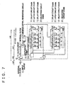
- Fig. 7 is a diagram illustrating a circuit arrangement according to a third example of the present invention.
- this example employs a scheme in which the delay circuit chain 11 for measuring the clock period tCK and the delay circuit chain 12 for reconstructing the measured period are arranged in the same direction and a pulse edge is propagated through the circuit.
- This scheme in which the delay circuit chain 11 and the delay circuit chain 12 for reconstructing the measured period are arranged in the same direction is such that a clock pulse edge propagates through the delay circuit chain 11 and the output of the delay circuit chain 12 is selected when the next clock pulse is output by the input buffer 13.
- This arrangement corresponds to the prior-art schemes set forth in literature (3) (Proc. of IEEE 1992 CICC 25.2) and in literature (2) (1996 Symp. on VLSI Circ., pp. 112 ⁇ 113) described above in connection with Fig. 13.
- a clock pulse edge is used in this embodiment, measurement of the clock period by the delay circuit 11 and measurement by the delay circuit 12 is not possible by the single delay circuit 11 and the single delay circuit 12. Accordingly, a clock having a duty of 50% must be prepared and use of the measurement and delay circuits must be repeated every half period, or it is necessary to provide two sets of the delay circuit chains and operate the sets alternately every period.
- two sets of the delay circuit chains are provided and the sets are operated alternately every period.
- the output of the input buffer 13 to which the external clock is applied is input to a 1/2 frequency divider 24, whereby the clock is frequency divided and then supplied to the two sets of delay circuit chains.
- the elements constituting the delay circuit 11 and delay circuit 12 construct clocked inverters.
- the clock pulse is not allowed to propagate through the delay circuit chain 11 by the signal D produced by the monitor signal generating circuit 19 from the input and output of the clock driver 14. This makes it possible to eliminate the clock driver dummy.
- the circuitry can be used as an ASIC macro in a manner similar to that of the first embodiment.
- Fig. 8 is a diagram illustrating a circuit arrangement according to a fourth example of the present invention.
- this example employs a scheme in which the delay circuit chain 11 for measuring the clock period tCK and the delay circuit chain 12 for reconstructing the measured period are arranged in opposite directions and a pulse edge is propagated through the circuit.
- This scheme in which the delay circuit chain 11 and the delay circuit chain 12 for reconstructing the measured period are arranged in opposite directions is such that a clock pulse edge travels through the delay circuit chain 11 and the output of the delay circuit chain 12 is selected when the next clock pulse is output by the input buffer 13.
- This arrangement corresponds to the prior-art scheme set forth in literature (4) (IEICE TRANS. ELECTRON., VOL. E79-C, No. 6, June, 1996, pp. 798 ⁇ 807) described above in connection with Fig. 11.
- the elements constituting the delay circuit 11 and delay circuit 12 construct clocked inverters.
- the clock pulse is not allowed to propagate through the delay circuit chain 11 by the signal D produced by the monitor signal generating circuit 19 from the input and output of the clock driver 14. This makes it possible to eliminate the clock driver dummy.
- the circuitry can be used as an ASIC macro in a manner similar to that of the first embodiment.
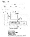
- Fig.17 shows the configuration of the second embodiment of the present invention
- Fig.18 shows the timing chart for illustrating the operation of the second embodiment and specifically illustrate the timing waveform of various components of Fig.1, respectively
- the second embodiment of the present invention includes a synchronous delay circuit made up of a delay circuit chain 1 for measuring a pre-set time interval and a delay circuit chain 2 for reproducing the measured delay time.
- the second embodiment also includes an input buffer 3, a clock driver 4, an input dummy 5 and a monitor signal generating circuit 9.
- the clock period is measured by allowing the clock signals to pass through the delay circuit chain 1 used for measurement.
- the clock signals are prohibited from proceeding through the delay circuit chain 1 to discontinue the measurement of the clock period tCK.
- the time during which signals are traveling through the delay circuit chain 1 is just equal to the clock period tCK less the sum of the delay time td2 of the input buffer 3 and the delay time td1 of the clock driver 4 ( tCK - (td1+td2), while the delay time reproduced by the delay circuit chain 2 is also tCK - (td1+td2).
- the monitor D is output during the time corresponding to the time exceeding the clock period tCK, that is the residual of the time corresponding to the quotient of the sum of the delay time of the clock driver 4 and that of the input dummy 5 divided by the clock period tCK to halt the signal in the delay circuit chain 1 used for measurement. That is, clock skew may be removed even if the sum of the delay time td1 of the clock driver 4 and the delay time td2 of the input dummy 5 is longer than the clock period tCK.
- the monitor signal D which halts the progress of the clock signals monitors the time period during which the clock pulses are traveling through the clock driver 4.
- the timing of passage through the clock driver 4 is quickened by tCK - (td1+td2) as from the time of clock synchronization.
- the monitor signal D is output twice during one clock period.
- a monitor signal D shown by hatching and a subsequent signal thereof are outputted. This can be evaded by methods such as
- a monitor signal D directly preceding the monitor signal D to be halted shown by hatching at D in Fig.1(C) in the first embodiment shown in Fig.1, is halted.
- the internal clock not freed of skew is output only once, such that the clock skew can be removed at a faster timing than with the above-described first embodiment.
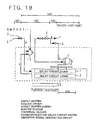
- Fig.19 shows the constitution of the fifth example of the present invention.
- Fig.20 shows a timing chart for illustrating the operation of the fifth example.
- the specific circuit structure of the delay circuits 1 and 2 are similar to that of each of the first to fourth examples.
- switching of the clock paths is performed by an external signal SMDACT entering the switching circuit 10 as a switching control signal.
- SMDACT is set to the low level and the operating mode is initiated
- the external clock signal 6 is allowed to pass through a path from the input buffer 3 through the switch 10 to the clock driver 4.
- An output of the clock driver 4 is once supplied as an internal clock 7, after which the pulse path from the input buffer 3 to the clock driver 4 is switched to the pulse path to the delay circuit chain 1. This generates the monitor signal D without waste.
- delay circuit chains 1, 2 are shown linearly, these may be arranged in a ring, as shown in JP Patent Kokai JP-A-8-237091, to cause rotation of the clock signals to permit the number of revolutions by a counter. This can be applied to all of the different forms of the delay circuits used in the first to fourth examples.
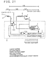
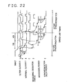
- Fig.21 shows the structure of a third embodiment of the present invention and Fig.22 shows a timing chart for illustrating the operation of the third embodiment of the present invention.
- the present third embodiment includes a synchronous delay circuit made up of a delay circuit chain 1 for estimating a pre-set time interval and a delay circuit chain 2 for reproducing the estimated delay time.
- the present third embodiment also includes an input buffer 3, a clock driver 4, an input buffer dummy 5, a monitor signal generating circuit 9 and first and second switches (changeover units) 10A, 10B.
- the first switch 10A switches between an output of the input buffer 3 and an output of the delay circuit chain 2 used for delay reproduction by the control signal SMDACT to send the selected signal to the clock driver 4 and to the monitor signal generating circuit 9.
- the second switch 10B is fed with an output of the input buffer 3 and an output of the input buffer dummy 5 to send one of the outputs to an input of the delay circuit chain 1 used for clock period measurement.
- the clock period is measured by allowing the clock signals to pass through the delay circuit chain 1 used for measuring the clock period.
- the delay circuit chain 1 used for measuring the clock period.
- passage of clock signals through the delay circuit chain 1 is inhibited to discontinue the measurement of the clock period tCK.
- the time during which signals are traveling through the delay circuit chain 1 is just equal to the clock period tCK less the sum of the delay time td2 of the input buffer 3 and the delay time td1 of the clock driver tCK - (td1+td2), while the delay time reproduced by the delay circuit chain 2 (synchronous delay time) assumes also tCK - (td1+td2).
- the monitor signal D is output during the time corresponding to the time exceeding the clock period tCK, that is the residual of the time corresponding to the quotient of the sum of the delay time of the clock driver 4 and that of the input driver 3 by the clock period to halt the progress of the signal in the delay circuit chain 1 used for measurement. That is, clock skew may be removed even if the sum of the delay time td1 of the clock driver 4 and the delay time td2 of the input dummy 5 is longer than the clock period tCK.
- the monitor signal D which halts the progress of the clock signals monitors the time period during which the clock pulses are traveling through the clock driver 4.
- the timing of passage through the clock driver 4 is quickened by tCK - (td1+td2) as from the time of clock synchronization.
- the clock signals pass through the input buffer 3, first switch 10A, clock driver 4 and the input dummy 5 before synchronization and are subsequently input to the measurement delay circuit chain 1 through the second switch 10B in order to measure the time of tCK- (td1+td2).
- the monitor signal D is output at the time of synchronization in order to measure the time of tCK - (td1+td2).
- Fig.21 shows a configuration of the third embodiment of the present invention and Fig.22 is a timing chart for illustrating the operation thereof.
- the specified structure of the delay circuit chains 1 and 2 are similar to that of the first to fourth examples described above.
- the clock path is switched by the external signal SMDACT (by SMDACT going low in Fig.22) to enter the operating mode and subsequently the external clock signal 6 is once furnished as the internal clock signal 7.
- the clock signals are then passed from the input buffer 3 to the clock driver 4.
- the time of tCK - (td1+td2) is measured by the clock pulses passing through the input buffer dummy 5 to enter the delay circuit chain 1 used for measurement.
- the clock signal path is changed to a path from the input buffer 3 and the second switch 10B which has selected an output of the input buffer 3 through the delay circuit chain 1 for measurement and the delay circuit chain 2 for delay reproduction to the first switch 10A which has selected the output of the input buffer 3 and to the clock driver 4 in order to remove the skew of the external clock 6 and the internal clock 7, that is in order to synchronize the two clocks.
- the monitor signal D is output to measure the time of tCK - (td1+td2).
- delay circuit chains 1 and 2 described above are of a linear configuration, these may also be arranged in a ring shape as already shown in JP Patent Kokai JP-A-8-237091, with the clock signals being rotated and the number of revolutions thereof being counted by a counter. This configuration may be applied to all sorts of the delay circuits used in the first to fourth embodiments.
- Fig.23 shows the configuration of the fourth embodiment of the present invention and Fig.24 is a timing chart for illustrating the operation of the fourth embodiment.
- the fourth embodiment of the present invention includes a synchronous delay circuit made up of a delay circuit chain 1 for measuring a pre-set time and a delay circuit chain 2 for reproducing the measured delay time.
- the fourth embodiment also includes an input buffer 3, a clock driver 4, an input buffer dummy 5 and a monitor signal generating circuit 9.
- the clock period is measured by passing the clock signals through the delay circuit chain 1 used for measurement.
- the period responsible for clock skew such as the period during which the clock pulses are travelinging through the clock driver 4 or the period during which the clock pulses are traveling through the input buffer dummy 5
- the clock signals are prohibited from being passed through the delay circuit chain 1 in order to discontinue the measurement of the clock period tCK.
- the period during which the clock signals traverse the delay circuit chain 1 is just equal to the clock period tCK less the sum of the delay time td2 of the input buffer 3 and the delay time td1 of the clock driver 4, that is tCK - (td1+td2).
- the delay time reproduced by the delay circuit chain 2 is also equal to tCK - (td1+td2).
- the circuit 9 for outputting the monitor signal D during the time the clock pulses are traveling through the input buffer 3 and the input buffer dummy 5 is constituted by a SR flipflop, and if the sum of the delay time in the clock driver 4 and that in the input dummy 5 is longer than the clock period tCK, the monitor signal D is output during the time equal to the time exceeding the clock period tCK, that is the residual of the quotient obtained on dividing the sum of the delay time td2 of the input buffer 3 and the delay time td1 of the clock driver 4, (td1+td2), by the clock period tCK, in order to halt the progress of the signal through the delay circuit chain 1 used for clock period measurement.
- tCK the delay time td2 of the input buffer 3 and the delay time td1 of the clock driver 4
- the monitor signal D which halts the progress of the clock signals, monitors the time period during which the clock pulses are passing through the clock driver 4, so that, since the time of clock synchronization, the timing of travel of the clock signals through the clock driver 4 is quickened by tCK-(td1+td2).
- the clock signals are passed at all times through the input buffer 3, delay circuit chains 1 and 2, clock driver 4 and the input buffer dummy 5.
- the clock signals subsequently enter the delay circuit chain 1 for measurement in order to measure and reproduce the clock period tCK, whereas, during synchronization, the clock signals cause the monitor signal D to be output in order to measure the time tCK-(td1+td2).
- the monitor signal may be output twice during one period by switching from the pre-synchronization state to the post-synchronization state, as in the first and second embodiments described above. It is noted that the measures used in the first and second embodiments for preventing outputting of the monitor signal D twice may be used as in the fourth embodiment of the present invention.
- the clock path (wiring length) can be reduced to render it possible to handle clock signals of a shorter period and a higher frequency.
- Fig.23 shows the configuration of the fourth embodiment of the present invention and Fig.24 is a timing chart for illustrating the operation of the fourth embodiment.
- the present embodiment again has delay circuit chains 1 and 2, the specified circuit structure of which is similar to that of the above-described first to fourth examples.
- clock signals are passed at all times through an input buffer 3, delay circuit chains 1 and 2, clock driver 4 and the input buffer dummy 5.
- a clock monitor signal D is generated after the synchronization operation mode is entered.
- the internal clocks free of clock skew are generated by measuring the time of tCK - (td1+td2) by the delay circuit chain 1 and by reproducing the time of tCK - (td1+td2) by the delay circuit chain 2.
- the delay circuit chain 1 is not in operation with the second clock monitor signal D or a clock monitor signal D following the second clock monitor signal D after a first clock monitor signal D is generated (monitor signal shown by hatching in Fig.24). This evades the monitor signal D acting twice on the delay circuit chain 1 during one period to generate tCK - (td1+td2) at all times.
- the delay circuit chains 1, 2 are not limited to the linear array of delay elements.
- these delay elements may also be arrayed in a ring so that the clock signals are rotated and the number of times of rotation may be counted by a counter.
- the delay circuits used in the first to fourth embodiments may be used without limitations.
- the double frequency internal clocks freed of clock skew and Duty50 clocks can be produced with the two clock periods for removing clock skew and 1.5 periods for the double frequency and the Duty50.
- this conventional internal delay circuit the removal of clock skew and the double frequency with Duty50 are achieved by two clock periods and 1.5 clock period in series, 3.5 clocks (3.5 tCK) are required for skew removal.
- Fig.27 shows the structure of the fifth embodiment of the present invention.
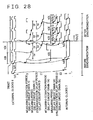
- Fig.28 is a timing chart for illustrating the operation of the fifth embodiment of the present invention.
- the fifth embodiment of the present invention includes, in addition to the input buffer 3, first switch 10A, clock driver 4, input dummy 5, monitor signal generating circuit 9 and the circuit configuration for skew removal comprised of the synchronous delay circuit made up of the delay circuit chain 1 for clock period measurement and the delay circuit chain 2 for clock period reproduction, a delay circuit chain 1A for measuring the pre-set time, a speed variable delay circuit chain 2A for reproducing the delay time proportionate to the measured delay time, a second switch 10B and a synthesis circuit 9A.
- An output (A) of the input buffer 3 and an output (E1) of the delay circuit chain 2 for clock period reproduction are input to the second switch 10B, an output of which is coupled to the delay circuit chain 1A used for measuring the pre-set time.
- An output of the delay circuit chain 2 and the speed variable delay circuit chain 2A for reproducing the delay time is input to the signal synthesis circuit 9A, an output of which is input to the first switch 10A.
- An output of the first switch 10A is sent to the clock driver 4 and the monitor signal generating circuit 9.
- the clock period is measured by passing the clock signals through the delay circuit chain 1A used for measuring clock periods. First, the clock periods are measured by an output of the input buffer 3 and when the signal E1 is output from the delay circuit chain 2 for period reproduction, the clock period is measured with the signal from the delay circuit chain 2.
- the speed variable delay circuit chain 2A adapted for reproducing the delay time proportionate to the measured delay time reproduces the delay time proportionate to the measured delay time no matter whether the delay circuit chain 1A used for measuring the period has measured the clock period by a signal from the delay circuit chain 2 selected by the second switch 10B or an output of the input buffer 3.
- the speed variable delay circuit chain 2A controls the output by the signal from the delay circuit chain 2. There is produced at this time a time difference during which the measurement of the clock period tCK is discontinued.
- the clock period can be measured by the delay circuit chain 1A, so that, when the clocks free of skew are output by the delay circuit chain 2, the generated clocks can be immediately passed through the delay circuit chain 2A having the delay proportionate to the clock period.
- Fig.27 shows the structure of an eighth example of the present invention and Fig.28 shows a timing chart for illustrating the operation of the eighth embodiment.
- the specified circuits of the delay circuit chains 1 and 2 and the delay circuit chains 1A and 2A can be configured similarly to those of the above-described first to fourth embodiments.
- the delay time of the delay circuit chain 2A for period reproduction is just a half that of the delay circuit chain 1A for period measurement.
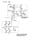
- the delay circuits of the period delay circuit chain 2A may be implemented by the number of elements, difference in driving capability and in delay time difference. Several examples of the circuit configuration are shown in Figs.29 to 32.
- the circuit of the eighth embodiment includes a delay circuit chain 11 for measurement, a control circuit 18 for controlling the transfer to a delay circuit chain 12 for delay reproduction of clocks propagated through the delay circuit chain 11 and the delay circuit chain 12.
- the number of elements (delay elements made up of NANDs and inverters) per stage is equal to that of the delay circuit chain 12.
- the delay time of the delay circuit chain 12 for period reproduction is just a half of that of the delay circuit chain 11 for period measurement.
- the delay circuits of the delay circuit chain 11 are configured for turning PMOS and NMOS transistors on and off based on the monitor signal D for controlling the on/off state of the NMOS transistors for controlling the active/inactive states of the delay circuits (NAND circuits and inverter circuits).
- the delay circuits of the delay circuit chain 12 are activated at all times.
- the number of loads of the delay circuits of the delay circuit chain 12 (NANDs for load adjustment) per stage is set to twice as many as that of the delay circuit chain 12.
- the driving capability per stage of the delay circuits of the delay circuit chain 12 is set to double that of the delay circuit chain 11. That is, two clocked inverters are connected in parallel per stage in the delay circuit chain 12. Each clocked inverter of the delay circuit chain 12 has its active or inactive state controlled by a complementary signal of a signal AA adapted for controlling the active or inactive state of the delay circuit chain 11.
- the driving capability per stage of the delay circuits of the delay circuit chain 12 is set to double that of the delay circuit chain 11.
- the delay circuit chain 11 is made up of two stages of clock inverters per stage of the delay circuit, while the delay circuit chain 12 is made up of two stages of parallel-connected clock inverters per stage of the delay circuit.
- the PMOS and NMOS transistors (such as MP12, MN12) controlling the activation/ non-activation of the clocked inverters of the period-measurement delay circuit chain 1 have gate terminals controlled a logical product (AND) output of the monitor signal D and a frequency divided signal AA of a signal A (external clock input) and its inverted value
- the PMOS and NMOS transistors adapted for controlling the activation/ non-activation of the clocked inverters of the delay circuit chain 12 for delay reproduction have gate terminals controlled by the complementary signal of the frequency divided signal and its inverted value.
- a modified embodiment PMOS transistors MP12 and MP12B of the first stage clocked inverter and NMOS transistors MN12 and MN12B of the second stage clocked inverter can be eliminated in the delay circuit chain 11 on the one hand.
- the parallel transistors MP13 and MP13a of the first stage clocked inverter and the parallel transistors MN13, MN13B and MN13C of the second stage clocked inverter can be eliminated.
- the clock signals received by the delay circuit chain 11 are driven alternately by PMOS transistors and NMOS transistors in a sequence of Fln- NMOS transistors-Fln+1- PMOS transistor- Fln+2....
- the PMOS transistors and NMOS transistors are driven likewise alternately. In such an arrangement, the required number of elements is reduced to about a half as compared to the case of Fig. 32.
- a further modification is also possible.
- PMOS and NMOS transistors functioning as switch elements and constituting the CMOS inverter are disposed inside / outside with respect to the power supply Vcc and the ground line GND in Fig.32.
- these PMOS and NMOS transistors constituting the CMOS inverter may be disposed between the switching element and Vcc, and between the switching element and GND, respectively.
- first and second delay circuit chains, third and fourth delay circuit chains may be made up of delay circuits adapted for separately driving PMOS and NMOS transistors constituting the delay circuit of the delay circuit chains.
- the single-phase clock signals are entered from outside in the above-described embodiments, it is possible with the present invention to use complementary clock signals as clocks 6 entered from outside and to utilize the rising and falling edges of the complementary clock signals. Since the distance traversed by the clock signals may be half the clock period, the circuit scale may be reduced.
- FIG.33 shows the structure of the ninth embodiment.
- the second switch 10B (changeover unit) of Fig.27 is omitted and an output of the first switch (changeover unit) 10B is sent to the clock driver 4, monitor signal generating circuit 9 and to the delay circuit chain 1A.
- Outputs of the delay circuit chain 2 and the delay circuit chain 2A are synthesized by a signal synthesis circuit 9A, with the synthesized signal being supplied from the first switch 10 via clock driver 4 as the internal clock.
- the switch 10 first selects the external clocks from the input buffer 3 to send the internal clock signals 7 from the clock driver 4. Outputs of the input buffer 3 are sent to the delay circuit chains 1, 2 and to the delay circuit chains 1A, 2A . After synchronization, an output of the signal synthesis circuit 9A is selected.
- delay circuit chains 1, 2, 1A and 2A are shown linearly, these may also be arranged in a ring, as disclosed in JP Patent Kokai JP-A-8-237091, with the clock signals being rotated and the number of times of rotation thereof being then counted by a counter. In this case, any of the delay circuits shown in examples 1 to 4 may be used.
- the period of a clock is measured as the propagation time of a clock pulse or clock pulse edge
- the amount of delay of a clock driver is measured by halting the propagation of a clock pulse
- a time obtained by excluding the amount of delay of the clock driver from the clock period is measured.
Landscapes
- Physics & Mathematics (AREA)
- Nonlinear Science (AREA)
- Pulse Circuits (AREA)
- Dram (AREA)
- Stabilization Of Oscillater, Synchronisation, Frequency Synthesizers (AREA)
- Synchronisation In Digital Transmission Systems (AREA)
Claims (29)
- Synchronverzögerungsschaltung zum Steuern eines Taktsignals mit:einer ersten Verzögerungsschaltungskette (11), die einen Puls oder eine Pulsflanke für eine feste Zeitspanne durchleitet, undeiner zweiten Verzögerungsschaltungskette (12), die einen Puls oder Pulsflanke über eine Länge durchlassen kann, die proportional zu der Länge der ersten Verzögerungsschaltungskette (11) ist, entlang der der Puls oder die Pulsflanke weitergeleitet wird, gekennzeichnet durcheine Schaltung (19) zum Ausgeben eines Überwachungssignals (D) für eine Zeitspanne, über der ein Taktpuls durch einen Takttreiber geleitet wird, wobei das Fortschreiten eines Pulses oder einer Pulskante in der ersten Verzögerungsschaltungskette (11) während der Ausgabe des Überwachungssignals (D) angehalten wird.
- Schaltung nach Anspruch 1, wobei Verzögerungsschaltungselemente, die die erste Verzögerungsschaltungskette bilden, durch getaktete Inverter gebildet sind, die durch das Überwachungssignal gesteuert werden.
- Integrierte Halbleiterschaltungsvorrichtung mit einer Synchronverzögerungsschaltung nach Anspruch 1, wobei ein Takttreiber (14) ein internes Taktsignal ausgibt.
- Vorrichtung nach Anspruch 3, wobei Verzögerungsschaltungselemente, die die erste Verzögerungsschaltungskette bilden, durch getaktete Inverter gebildet sind, die durch das Überwachungssignal gesteuert werden.
- Vorrichtung nach Anspruch 3 oder 4 mit einem Schalter (10), der zwischen einem Ausgang eines Eingabepuffers (13), an den das externe Taktsignal als Eingabe angelegt wird, und einem Ausgang der zweiten Verzögerungsschaltungskette (12) schaltet und die Ausgabe an den Takttreiber (14) liefert.
- Vorrichtung nach Anspruch 3, wobei die Überwachungssignal-Erzeugungsschaltung (19) ein Flip-Flop aufweist, das durch eine Eingabe und eine Ausgabe des Takttreibers (14) rückgesetzt bzw. gesetzt wird.
- Integrierte Halbleiterschaltungsvorrichtung mit der Synchronverzögerungsschaltung nach Anspruch 1 als Makro, wobei
das Taktsignal von der ersten Verzögerungsschaltungskette (11) als eine Eingabe an die zweite Verzögerungsschaltungskette (12) angelegt wird und
der Takttreiber (14) ein internes Taktsignal abgibt und mit
einem Schalter (10), der zwischen einem Ausgang eines Eingangspuffers (13) und einem Ausgang der zweiten Verzögerungsschaltungskette (12) schaltet. - Vorrichtung nach Anspruch 7, wobei die erste Verzögerungsschaltungskette (11) und die zweite Verzögerungsschaltungskette (12) unter Berücksichtigung ihrer Signalfortpflanzungsrichtungen in entgegengesetzten Richtungen angeordnet sind und wobei ein Taktpuls durch die erste Verzögerungsschaltungskette weitergeleitet wird und anschließend in die zweite Verzögerungsschaltungskette über eine Steuerschaltung (18) gelangt, wenn der nächste Taktpuls durch den Eingangspuffer (13) ausgegeben wird.
- Vorrichtung nach Anspruch 7, wobei die erste Verzögerungsschaltungskette (11) und die zweite Verzögerungsschaltungskette (12) im Hinblick auf ihre Signalfortpflanzungsrichtungen in entgegengesetzten Richtungen angeordnet sind und wobei ein Taktsignal durch die erste Verzögerungsschaltungskette weitergeleitet wird und dann in die zweite Verzögerungsschaltungskette gelangt, wenn der nächste Taktpuls durch den Eingangspuffer (13) ausgegeben wird.
- Vorrichtung nach Anspruch 7, wobei die erste Verzögerungsschaltungskette (11) und die zweite Verzögerungsschaltungskette im Hinblick auf ihre Signalfortpflanzungsrichtungen in derselben Richtung angeordnet sind, wobei ein Taktsignal durch die erste Verzögerungsschaltungskette geleitet wird und der Ausgang der zweiten Verzögerungsschaltungskette ausgewählt wird, wenn der nächste Taktpuls durch den Eingangspuffer (13) ausgegeben wird.
- Vorrichtung nach Anspruch 7, wobei die erste Verzögerungsschaltungskette (11) und die zweite Verzögerungsschaltungskette (12) im Hinblick auf ihre Signalfortpflanzungsrichtungen in entgegengesetzten Richtungen angeordnet sind, wobei ein Taktsignal durch die erste Verzögerungsschaltungskette geleitet wird und der Ausgang der zweiten Verzögerungsschaltungskette ausgewählt wird, wenn der nächste Taktpuls durch den Eingangspuffer ausgegeben wird.
- Integrierte Halbleiterschaltung nach Anspruch 7, wobei der Schalter (10) nach der ersten Ausgabe eines Überwachungssignals (D) für die Überwachungssignal-Erzeugungsschaltung (19) zwischen dem Ausgang eines Eingangspuffers (13), der Taktsignale von außerhalb erhält, und dem Ausgang der zweiten Verzögerungsschaltung (12) schaltet.
- Integrierte Halbleiterschaltung nach Anspruch 7, wobei der Schalter (10) die ausgewählte Ausgabe an den Takttreiber (14) liefert, wobei
während des Schaltungsbetriebs die externen Taktsignale veranlasst werden, durch einen Pfad von dem Eingangspuffer (13) durch den Schalter (10) bis zu dem Takttreiber (14) zu laufen, wobei eine Ausgabe des Takttreibers (14) einmalig als interne Takte geliefert wird und anschließend der Pfad von dem Eingangspuffer (13) zum Takttreiber (14) geschaltet wird zu dem Pfad von dem Eingangspuffer (13) zu der ersten Verzögerungsschaltungskette (11), wobei eine Ausgabe der zweiten Verzögerungsschaltungskette (12) durch den Schalter (10) so ausgewählt wird, dass sie als interne Taktsignale durch den Takttreiber (14) geliefert werden. - Integrierte Halbleiterschaltung nach Anspruch 7, wobei die Steuerung durchgeführt wird, um das nächste Überwachungssignal (D) nach dem ersten Ausgeben des Überwachungssignals, zu stoppen.
- Integrierte Halbleiterschaltung nach einem der Ansprüche 7 bis 14 mit ferner:wobei die Überwachungssignal-Erzeugungsschaltung (19) Überwachungssignale während einer Spanne ausgibt, in der Taktsignale durch den Takttreiber (14) und den Eingangspuffer (13) weitergeleitet werden.einer Eingabepuffer-Dummyschaltung (15) mit einer Verzögerungszeit, die gleich der des Eingangspuffers (13) ist, der externe Taktsignale erhält, wobei der Takttreiber (14) und die Eingangspuffer-Dummyschaltung (15) in Reihe miteinander geschaltet sind,
- Integrierte Halbleiterschaltung nach Anspruch 15 mit ferner:wobei der zweite Schalter eine Ausgabe des Eingangspuffers (3) als einen ersten Taktpuls oder als eine Pulsflanke ausgibt, die in die erste Verzögerungsschaltungskette (1) gelangt.einem zweiten Schalter (10B) zum Schalten zwischen einer Ausgabe der Eingangspuffer-Dummyschaltung (5) und einer Ausgabe des Eingangspuffers (3), wobei die Ausgabe des zweiten Schalters (10B) an die erste Verzögerungsschaltungskette (1) geliefert wird,
- Synchronverzögerungsschaltung nach Anspruch 16, wobei während des Schaltungsbetriebs zunächst verursacht wird, dass die externen Taktsignale durch einen Pfad von dem Eingangspuffer (3) durch den ersten Schalter (10A) zu dem Takttreiber (4) laufen, wobei die Ausgabe des Takttreibers einmalig als interne Takte geliefert wird und anschließend Taktsignale von ausserhalb dazu veranlasst werden, durch einen Pfad von dem Eingangspuffer (3) zu dem Takttreiber (4) zu laufen, wobei die Zeit entsprechend dem Unterschied der Summe (td1 + td2) einer Verzögerungszeit (td1) des Eingangspuffers (3) und einer Verzögerungszeit (td2) des Takttreibers (4), die von einer Taktzeitspanne (tCK) abgezogen wird, durch Durchlauf der Taktsignale durch die Eingangspuffer-Dummyschaltung (5) und anschließend von dem zweiten Schalter (10B) zu der ersten Verzögerungsschaltungskette (1) gemessen wird, und
wobei vom nächsten Taktsignal an der Verlaufspfad geschaltet wird, von einem Pfad über den Eingangspuffer (3) und den zweiten Schalter (10B), durch die erste Verzögerungsschaltungskette (1) für die Messung und die zweite Verzögerungsschaltungskette (2) für die Verzögerungsreproduktion, zu einem Pfad über den ersten Schalter (10A) und dem Takttreiber (4) zum Entfernen des Versatzes der internen Takte und der externen Takte. - Integrierte Halbleiterschaltung nach einem der Ansprüche 3 bis 17 mit ferner:wobei Takte für eine optionale Zeitspanne angehalten werden können, nachdem ihnen ermöglicht wurde, durch die dritte Verzögerungsschaltungskette (1A) durchzulaufen.einer dritten Verzögerungsschaltungskette (1A) zum Ermöglichen, dass Pulse oder Pulsflanken für eine Vorgabezeit fortschreiten, undeiner vierten Verzögerungsschaltungskette (2A), die es ermöglicht, dass die Pulse oder Pulskanten durch eine Länge durchlaufen, die proportional ist zu der Länge, durch die die Pulse oder Pulskanten in der dritten Verzögerungsschaltungskette (1A) durchgelaufen sind,
- Integrierte Halbleiterschaltung nach Anspruch 18 mit ferner:einem dritten Schalter (10, 10B), der zwischen einem Ausgang eines Eingangspuffers (3), der externe Takte erhält, und einem Ausgang der zweiten Verzögerungsschaltungskette (2) schaltet, wobei eine Ausgabe des dritten Schalters in die dritte Verzögerungsschaltungskette (1A) eintritt.
- Synchronverzögerungsschaltung nach Anspruch 1, wobei
die erste Verzögerungsschaltungskette es ermöglicht, dass Eingangstaktsignale, die von dem Eingangspuffer (3) ausgegeben werden, für eine Vorgabezeitspanne fortschreiten,
wobei die zweite Verzögerungsschaltungskette (3) Taktsignale von der ersten Verzögerungsschaltungskette (1) eingibt, die zweite Verzögerungsschaltungskette (2) es den eingegebenen Taktsignalen ermöglicht sie in einer Länge zu passieren, die der Länge der ersten Verzögerungsschaltungskette (1) entspricht, durch die die Signale durchgelaufen sind,
wobei die Überwachungssignalerzeugungsschaltung das Überwachungssignal während einer Zeitspanne ausgibt, in der die Eingabetaktsignale durch den Takttreiber (4) durchlaufen, interne Taktsignale ausgibt und durch eine Eingangspuffer-Dummyschaltung (5), die mit dem Takttreiber (4) verbunden ist, und mit ferner
einer dritten Verzögerungsschaltungskette (1A), die es ermöglicht, dass Pulse oder Pulskanten für eine Vorgabezeitspanne durchlaufen,
einer vierten Verzögerungsschaltungskette (2A) mit variabler Geschwindigkeit, die es ermöglicht, dass Pulse oder Pulskanten durch eine Länge durchlaufen, die proportional ist zu der Länge, durch welche die Pulse oder Pulskanten die dritte Verzögerungsschaltungskette (1A) durchlaufen haben,
einer Signalsyntheseschaltung (9A), die alle Ausgaben der zweiten Verzögerungsschaltungskette und eine Ausgabe der vierten Verzögerungsschaltungskette synthetisiert,
einem ersten Schalter (10A), an dem eine Ausgabe der Signalsyntheseschaltung (9A) und eine Ausgabe des Eingangspuffers (3) als Eingabe eingegeben werden, wobei der erste Schalter (10A) eine der Eingaben an den Takttreiber (4) und die Überwachungssignal-Erzeugungsschaltung (9) ausgibt, und
einem zweiten Schalter (10B), der eine Ausgabe des Eingangspuffers (3) und einer Ausgabe der zweiten Verzögerungsschaltung (2) als Eingabe empfängt, wobei der zweite Schalter eine der Ausgaben als eine Eingabe der dritten Verzögerungsschaltungskette (1A) ausgibt. - Synchronverzögerungsschaltung nach Anspruch 1, wobei
die erste Verzögerungsschaltungskette es Eingangstaktsignalen ermöglicht, die von dem Eingangspuffer (3) gesendet wurden, für eine Vorgabezeitspanne fortzuschreiten,
die zweite Verzögerungsschaltungskette (2) die Taktsignale von der ersten Verzögerungsschaltungskette (1) empfängt, wobei die zweite Verzögerungsschaltungskette (2) es Eingangstaktsignalen ermöglicht, für eine Länge zu passieren, die proportional zu der Länge der ersten Verzögerungsschaltungskette (1) ist, durch die die Taktsignale gelaufen sind,
wobei die Überwachungssignalerzeugungsschaltung das Überwachungssignal während einer Zeitspanne ausgibt, in der die Eingangstaktsignale durch den Takttreiber (4) laufen, der interne Taktsignale ausgibt, und durch eine Eingangspuffer-Dummyschaltung (5), die mit dem Takttreiber (4) verbunden ist, und mit ferner
einer dritten Verzögerungsschaltungskette (1A), die es ermöglicht, dass Pulse oder Pulsflanken sie für eine Vorgabezeitspanne durchlaufen, einer vierten Verzögerungsschaltungskette (2A) mit variabler Geschwindigkeit, die es ermöglichen kann, dass Pulse oder Pulsflanken durch sie für eine Länge verlaufen, die proportional zu der Länge ist, durch die die Pulse oder Pulsflanken in der dritten Verzögerungsschaltungskette (1A) fortschreiten,
einer Signalsyntheseschaltung (9A), die eine Ausgabe der zweiten Verzögerungsschaltungskette und eine Ausgabe der vierten Verzögerungsschaltungskette synthetisiert, und
einem Schalter, der eine Ausgabe der Signalsyntheseschaltung (9A) und eine Ausgabe des Eingabepuffers (3) erhält, wobei der Schalter (10A) eine der Ausgaben an den Takttreiber (4), die Überwachungssignal-Erzeugungsschaltung (9) und die dritte Verzögerungschaltungskette (1A) ausgibt. - Integrierte Halbleiterschaltung nach einem der Ansprüche 18 bis 21, wobei die Verzögerungsschaltungselemente der dritten Verzögerungsschaltungskette (1A) und die der vierten Verzögerungsschaltungskette (2A) in einem gegenseitig unterschiedlichen Elementzahlverhältniss vorgesehen sind.
- Integrierte Halbleiterschaltung nach einem der Ansprüche 18 - 21, wobei die Verzögerungsschaltungselemente der dritten Verzögerungsschaltungskette (1A) und die der vierten Verzögerungsschaltungskette (2A) mit einem gegenseitig unterschiedlichen Lastverhältniss vorgesehen sind.
- Integrierte Halbleiterschaltung nach einem der Ansprüche 18 bis 21, wobei die Verzögerungsschaltungselemente der dritten Verzögerungsschaltungskette (1A) und der vierten Verzögerungsschaltungskette (2A) in einem gegenseitig unterschiedlichen Treiberkapazitätsverhältniss vorgesehen sind.
- Integrierte Halbleiterschaltung nach einem der Ansprüche 18 bis 21, wobei die erste, die zweite, die dritte und die vierte Verzögerungsschaltungskette (1, 2, 1A, 2A) aus Verzögerungsschaltungen aufgebaut sind, die für separate Treiber von PMOS- und NMOS-Transistoren angepasst sind, die Verzögerungsschaltungen der Verzögerungsschaltungsketten bilden.
- Integrierte Halbleiterschaltung nach einem der Ansprüche 18 bis 21, wobei das Taktsignal, das in die Verzögerungsschaltungskette eintritt, abwechselnd durch PMOS-Transistoren und NMOS-Transistoren in Reihe geteilt wird.
- Integrierte Halbleiterschaltung nach einem der Ansprüche 3 bis 25, wobei die Taktpulse oder Taktflanken, die von außen eindringen, komplementäre Taktsignale sind und wobei ansteigende oder abfallende Flanken der komplementären Taktsignale abwechselnd ausgenutzt werden.
- Integrierte Halbleiterschaltung nach einem der Ansprüche 3 bis 25, wobei die Taktpulse oder Taktflanken, die von außen eintreten, komplementäre Taktsignale sind und wobei zwei Sätze von Schaltungen vorgesehen sind, die reziprok eine ansteigende oder abfallende Flanke der komplementären Taktsignale verwenden.
- Integrierte Halbleiterschaltung nach einem der Ansprüche 8 bis 21, wobei zumindest eine der Verzögerungsschaltungsketten so konfiguriert ist, dass Verzögerungselemente in einem Ring aufgereiht sind, Taktsignale rotieren und die Anzahl der Male der Rotation durch einen Zähler gezählt wird.
Applications Claiming Priority (6)
| Application Number | Priority Date | Filing Date | Title |
|---|---|---|---|
| JP15797497 | 1997-05-30 | ||
| JP15797497 | 1997-05-30 | ||
| JP157974/97 | 1997-05-30 | ||
| JP14223498 | 1998-05-08 | ||
| JP10142234A JP3072726B2 (ja) | 1997-05-30 | 1998-05-08 | 同期遅延回路 |
| JP142234/98 | 1998-05-08 |
Publications (2)
| Publication Number | Publication Date |
|---|---|
| EP0896432A1 EP0896432A1 (de) | 1999-02-10 |
| EP0896432B1 true EP0896432B1 (de) | 2003-07-23 |
Family
ID=26474303
Family Applications (1)
| Application Number | Title | Priority Date | Filing Date |
|---|---|---|---|
| EP98109781A Expired - Lifetime EP0896432B1 (de) | 1997-05-30 | 1998-05-28 | Synchrone Verzögerungsschaltung |
Country Status (5)
| Country | Link |
|---|---|
| EP (1) | EP0896432B1 (de) |
| JP (1) | JP3072726B2 (de) |
| KR (1) | KR100310880B1 (de) |
| DE (1) | DE69816538T2 (de) |
| TW (1) | TW379482B (de) |
Families Citing this family (4)
| Publication number | Priority date | Publication date | Assignee | Title |
|---|---|---|---|---|
| JP3386031B2 (ja) * | 2000-03-06 | 2003-03-10 | 日本電気株式会社 | 同期遅延回路及び半導体集積回路装置 |
| KR100399973B1 (ko) * | 2001-06-30 | 2003-09-29 | 주식회사 하이닉스반도체 | 레지스터 제어 지연고정루프의 지연 모니터 및 그의 지연라인 제어 방법 |
| JP6296932B2 (ja) * | 2014-07-18 | 2018-03-20 | 株式会社東芝 | 遅延回路 |
| US12041713B2 (en) * | 2017-08-23 | 2024-07-16 | Teradyne, Inc. | Reducing timing skew in a circuit path |
Family Cites Families (2)
| Publication number | Priority date | Publication date | Assignee | Title |
|---|---|---|---|---|
| TW288232B (de) * | 1994-12-20 | 1996-10-11 | Nippon Electric Co | |
| TW350166B (en) * | 1996-09-13 | 1999-01-11 | Nippon Elecric Co | Multiple synchroneous delay circuit |
-
1998
- 1998-05-08 JP JP10142234A patent/JP3072726B2/ja not_active Expired - Fee Related
- 1998-05-28 DE DE69816538T patent/DE69816538T2/de not_active Expired - Lifetime
- 1998-05-28 EP EP98109781A patent/EP0896432B1/de not_active Expired - Lifetime
- 1998-05-29 TW TW87108580A patent/TW379482B/zh not_active IP Right Cessation
- 1998-05-30 KR KR1019980020133A patent/KR100310880B1/ko not_active Expired - Fee Related
Also Published As
| Publication number | Publication date |
|---|---|
| DE69816538T2 (de) | 2004-05-13 |
| JP3072726B2 (ja) | 2000-08-07 |
| DE69816538D1 (de) | 2003-08-28 |
| JPH1173238A (ja) | 1999-03-16 |
| KR19980087542A (ko) | 1998-12-05 |
| EP0896432A1 (de) | 1999-02-10 |
| KR100310880B1 (ko) | 2001-11-15 |
| TW379482B (en) | 2000-01-11 |
Similar Documents
| Publication | Publication Date | Title |
|---|---|---|
| US6075395A (en) | Synchronous delay circuit | |
| US6396320B2 (en) | Clock control method and circuit | |
| US6313676B1 (en) | Synchronous type semiconductor integrated circuit having a delay monitor controlled by a delay control signal obtained in a delay measuring mode | |
| EP1189348B1 (de) | Verfahren und Schaltung zur Taktsteuerung | |
| KR100393543B1 (ko) | 클럭제어방법 및 그 회로 | |
| JP3333429B2 (ja) | 半導体集積回路 | |
| KR100395467B1 (ko) | 동기 지연회로 및 반도체 집적회로 장치 | |
| KR100342896B1 (ko) | 동기 지연 회로 | |
| US5644499A (en) | Retiming gated-clocks and precharged circuit structures | |
| JP3986103B2 (ja) | 半導体集積回路 | |
| EP0896432B1 (de) | Synchrone Verzögerungsschaltung | |
| US6504414B2 (en) | Clock control method and circuit | |
| US6608514B1 (en) | Clock signal generator circuit and semiconductor integrated circuit with the same circuit | |
| EP0865160B1 (de) | Interpolationsschaltung | |
| JP4657053B2 (ja) | タイミング発生器及び半導体試験装置 | |
| US6333659B1 (en) | Clock control method and circuit | |
| EP0461291A1 (de) | Takterzeugung in einem Mehrchip-Rechnersystem | |
| JP3754028B2 (ja) | 半導体装置 |
Legal Events
| Date | Code | Title | Description |
|---|---|---|---|
| PUAI | Public reference made under article 153(3) epc to a published international application that has entered the european phase |
Free format text: ORIGINAL CODE: 0009012 |
|
| AK | Designated contracting states |
Kind code of ref document: A1 Designated state(s): DE FR GB |
|
| AX | Request for extension of the european patent |
Free format text: AL;LT;LV;MK;RO;SI |
|
| 17P | Request for examination filed |
Effective date: 19990311 |
|
| AKX | Designation fees paid |
Free format text: DE FR GB |
|
| 17Q | First examination report despatched |
Effective date: 20000703 |
|
| GRAH | Despatch of communication of intention to grant a patent |
Free format text: ORIGINAL CODE: EPIDOS IGRA |
|
| GRAH | Despatch of communication of intention to grant a patent |
Free format text: ORIGINAL CODE: EPIDOS IGRA |
|
| RAP1 | Party data changed (applicant data changed or rights of an application transferred) |
Owner name: NEC ELECTRONICS CORPORATION |
|
| GRAA | (expected) grant |
Free format text: ORIGINAL CODE: 0009210 |
|
| AK | Designated contracting states |
Designated state(s): DE FR GB |
|
| REG | Reference to a national code |
Ref country code: GB Ref legal event code: FG4D |
|
| REF | Corresponds to: |
Ref document number: 69816538 Country of ref document: DE Date of ref document: 20030828 Kind code of ref document: P |
|
| ET | Fr: translation filed | ||
| PLBE | No opposition filed within time limit |
Free format text: ORIGINAL CODE: 0009261 |
|
| STAA | Information on the status of an ep patent application or granted ep patent |
Free format text: STATUS: NO OPPOSITION FILED WITHIN TIME LIMIT |
|
| 26N | No opposition filed |
Effective date: 20040426 |
|
| REG | Reference to a national code |
Ref country code: FR Ref legal event code: CD |
|
| REG | Reference to a national code |
Ref country code: DE Ref legal event code: R082 Ref document number: 69816538 Country of ref document: DE Representative=s name: GLAWE DELFS MOLL - PARTNERSCHAFT VON PATENT- U, DE |
|
| REG | Reference to a national code |
Ref country code: DE Ref legal event code: R082 Ref document number: 69816538 Country of ref document: DE Representative=s name: GLAWE DELFS MOLL PARTNERSCHAFT MBB VON PATENT-, DE Effective date: 20120828 Ref country code: DE Ref legal event code: R082 Ref document number: 69816538 Country of ref document: DE Representative=s name: GLAWE DELFS MOLL - PARTNERSCHAFT VON PATENT- U, DE Effective date: 20120828 Ref country code: DE Ref legal event code: R081 Ref document number: 69816538 Country of ref document: DE Owner name: RENESAS ELECTRONICS CORPORATION, KAWASAKI-SHI, JP Free format text: FORMER OWNER: NEC ELECTRONICS CORP., KAWASAKI, KANAGAWA, JP Effective date: 20120828 Ref country code: DE Ref legal event code: R081 Ref document number: 69816538 Country of ref document: DE Owner name: RENESAS ELECTRONICS CORPORATION, JP Free format text: FORMER OWNER: NEC ELECTRONICS CORP., KAWASAKI, JP Effective date: 20120828 |
|
| PGFP | Annual fee paid to national office [announced via postgrant information from national office to epo] |
Ref country code: GB Payment date: 20130522 Year of fee payment: 16 Ref country code: DE Payment date: 20130522 Year of fee payment: 16 |
|
| PGFP | Annual fee paid to national office [announced via postgrant information from national office to epo] |
Ref country code: FR Payment date: 20130531 Year of fee payment: 16 |
|
| REG | Reference to a national code |
Ref country code: DE Ref legal event code: R119 Ref document number: 69816538 Country of ref document: DE |
|
| GBPC | Gb: european patent ceased through non-payment of renewal fee |
Effective date: 20140528 |
|
| REG | Reference to a national code |
Ref country code: FR Ref legal event code: ST Effective date: 20150130 |
|
| REG | Reference to a national code |
Ref country code: DE Ref legal event code: R119 Ref document number: 69816538 Country of ref document: DE Effective date: 20141202 |
|
| PG25 | Lapsed in a contracting state [announced via postgrant information from national office to epo] |
Ref country code: DE Free format text: LAPSE BECAUSE OF NON-PAYMENT OF DUE FEES Effective date: 20141202 |
|
| PG25 | Lapsed in a contracting state [announced via postgrant information from national office to epo] |
Ref country code: FR Free format text: LAPSE BECAUSE OF NON-PAYMENT OF DUE FEES Effective date: 20140602 Ref country code: GB Free format text: LAPSE BECAUSE OF NON-PAYMENT OF DUE FEES Effective date: 20140528 |