EP0896434A1 - Circuit de boucle à verrouillage de phase - Google Patents
Circuit de boucle à verrouillage de phase Download PDFInfo
- Publication number
- EP0896434A1 EP0896434A1 EP98114841A EP98114841A EP0896434A1 EP 0896434 A1 EP0896434 A1 EP 0896434A1 EP 98114841 A EP98114841 A EP 98114841A EP 98114841 A EP98114841 A EP 98114841A EP 0896434 A1 EP0896434 A1 EP 0896434A1
- Authority
- EP
- European Patent Office
- Prior art keywords
- voltage
- signal
- controlled oscillator
- frequency
- pll circuit
- Prior art date
- Legal status (The legal status is an assumption and is not a legal conclusion. Google has not performed a legal analysis and makes no representation as to the accuracy of the status listed.)
- Withdrawn
Links
- 239000003990 capacitor Substances 0.000 claims abstract description 38
- 230000003111 delayed effect Effects 0.000 claims abstract description 10
- 238000010586 diagram Methods 0.000 description 13
- 102100040678 Programmed cell death protein 1 Human genes 0.000 description 8
- 101710089372 Programmed cell death protein 1 Proteins 0.000 description 8
- 238000013459 approach Methods 0.000 description 2
- 238000007792 addition Methods 0.000 description 1
- BNPSSFBOAGDEEL-UHFFFAOYSA-N albuterol sulfate Chemical compound OS(O)(=O)=O.CC(C)(C)NCC(O)C1=CC=C(O)C(CO)=C1.CC(C)(C)NCC(O)C1=CC=C(O)C(CO)=C1 BNPSSFBOAGDEEL-UHFFFAOYSA-N 0.000 description 1
- 238000006243 chemical reaction Methods 0.000 description 1
- 230000000593 degrading effect Effects 0.000 description 1
- 238000000034 method Methods 0.000 description 1
- 239000010453 quartz Substances 0.000 description 1
- 230000000754 repressing effect Effects 0.000 description 1
- VYPSYNLAJGMNEJ-UHFFFAOYSA-N silicon dioxide Inorganic materials O=[Si]=O VYPSYNLAJGMNEJ-UHFFFAOYSA-N 0.000 description 1
Images



Classifications
-
- H—ELECTRICITY
- H03—ELECTRONIC CIRCUITRY
- H03L—AUTOMATIC CONTROL, STARTING, SYNCHRONISATION OR STABILISATION OF GENERATORS OF ELECTRONIC OSCILLATIONS OR PULSES
- H03L7/00—Automatic control of frequency or phase; Synchronisation
- H03L7/06—Automatic control of frequency or phase; Synchronisation using a reference signal applied to a frequency- or phase-locked loop
- H03L7/08—Details of the phase-locked loop
- H03L7/099—Details of the phase-locked loop concerning mainly the controlled oscillator of the loop
- H03L7/0991—Details of the phase-locked loop concerning mainly the controlled oscillator of the loop the oscillator being a digital oscillator, e.g. composed of a fixed oscillator followed by a variable frequency divider
- H03L7/0992—Details of the phase-locked loop concerning mainly the controlled oscillator of the loop the oscillator being a digital oscillator, e.g. composed of a fixed oscillator followed by a variable frequency divider comprising a counter or a frequency divider
-
- H—ELECTRICITY
- H03—ELECTRONIC CIRCUITRY
- H03L—AUTOMATIC CONTROL, STARTING, SYNCHRONISATION OR STABILISATION OF GENERATORS OF ELECTRONIC OSCILLATIONS OR PULSES
- H03L7/00—Automatic control of frequency or phase; Synchronisation
- H03L7/06—Automatic control of frequency or phase; Synchronisation using a reference signal applied to a frequency- or phase-locked loop
- H03L7/16—Indirect frequency synthesis, i.e. generating a desired one of a number of predetermined frequencies using a frequency- or phase-locked loop
- H03L7/18—Indirect frequency synthesis, i.e. generating a desired one of a number of predetermined frequencies using a frequency- or phase-locked loop using a frequency divider or counter in the loop
- H03L7/183—Indirect frequency synthesis, i.e. generating a desired one of a number of predetermined frequencies using a frequency- or phase-locked loop using a frequency divider or counter in the loop a time difference being used for locking the loop, the counter counting between fixed numbers or the frequency divider dividing by a fixed number
- H03L7/187—Indirect frequency synthesis, i.e. generating a desired one of a number of predetermined frequencies using a frequency- or phase-locked loop using a frequency divider or counter in the loop a time difference being used for locking the loop, the counter counting between fixed numbers or the frequency divider dividing by a fixed number using means for coarse tuning the voltage controlled oscillator of the loop
-
- H—ELECTRICITY
- H03—ELECTRONIC CIRCUITRY
- H03L—AUTOMATIC CONTROL, STARTING, SYNCHRONISATION OR STABILISATION OF GENERATORS OF ELECTRONIC OSCILLATIONS OR PULSES
- H03L7/00—Automatic control of frequency or phase; Synchronisation
- H03L7/06—Automatic control of frequency or phase; Synchronisation using a reference signal applied to a frequency- or phase-locked loop
- H03L7/08—Details of the phase-locked loop
- H03L7/085—Details of the phase-locked loop concerning mainly the frequency- or phase-detection arrangement including the filtering or amplification of its output signal
- H03L7/089—Details of the phase-locked loop concerning mainly the frequency- or phase-detection arrangement including the filtering or amplification of its output signal the phase or frequency detector generating up-down pulses
- H03L7/0891—Details of the phase-locked loop concerning mainly the frequency- or phase-detection arrangement including the filtering or amplification of its output signal the phase or frequency detector generating up-down pulses the up-down pulses controlling source and sink current generators, e.g. a charge pump
-
- H—ELECTRICITY
- H03—ELECTRONIC CIRCUITRY
- H03L—AUTOMATIC CONTROL, STARTING, SYNCHRONISATION OR STABILISATION OF GENERATORS OF ELECTRONIC OSCILLATIONS OR PULSES
- H03L7/00—Automatic control of frequency or phase; Synchronisation
- H03L7/06—Automatic control of frequency or phase; Synchronisation using a reference signal applied to a frequency- or phase-locked loop
- H03L7/16—Indirect frequency synthesis, i.e. generating a desired one of a number of predetermined frequencies using a frequency- or phase-locked loop
- H03L7/18—Indirect frequency synthesis, i.e. generating a desired one of a number of predetermined frequencies using a frequency- or phase-locked loop using a frequency divider or counter in the loop
- H03L7/197—Indirect frequency synthesis, i.e. generating a desired one of a number of predetermined frequencies using a frequency- or phase-locked loop using a frequency divider or counter in the loop a time difference being used for locking the loop, the counter counting between numbers which are variable in time or the frequency divider dividing by a factor variable in time, e.g. for obtaining fractional frequency division
- H03L7/1972—Indirect frequency synthesis, i.e. generating a desired one of a number of predetermined frequencies using a frequency- or phase-locked loop using a frequency divider or counter in the loop a time difference being used for locking the loop, the counter counting between numbers which are variable in time or the frequency divider dividing by a factor variable in time, e.g. for obtaining fractional frequency division for reducing the locking time interval
Definitions
- the present invention relates to a phase locked loop (PLL) circuit.
- PLL phase locked loop
- Phase detector (PD) 1 accepts an external input signal frequency fi and a feedback signal frequency f 0 /N which is generated by multiplying the output signal frequency f 0 from voltage controlled oscillator (VCO) 4 by 1/N in frequency divider 5.
- PD 1 compares the frequencies and phases of fi and f 0 /N and then, outputs pulse signals PU and PD corresponding to the differences between them. Then, the outputs from PD 1 are fed into charge pump 2.
- Charge pump 2 converts the pulse signals PU and PD into analog quantities and outputs them to low pass filter (LPF) 3.
- LPF 3 eliminates the high frequency component and noise in the output signal from charge pump 2 and output it as V 0 to VCO 4.
- VCO 4 outputs the output signal frequency f 0 .
- the output signal frequency f 0 multiplied by 1/N in frequency divider 5 is fed back into PD 1.
- the PLL circuit repeats these operations and stabilizes the frequency output of the input signal frequency fi multiplied by N, when the input signal fi becomes equal to the feedback signal frequency f 0 /N.
- it is desirable to shorten the time (pull- in time) required to lock the PLL circuit until fi becomes equal to f 0 /N because the PLL circuit is a kind of frequency negative feedback circuit which acts to detect the differences of the phases between the input signal and the feed-back signal. Therefore, there is disclosed, for example, in the Japanese Patent laid-open No. Hei 8-228148 (1996), a technique wherein the time (lock-in time) required to lock the PLL circuit can be reduced, when the input signal frequency is changed.
- FIG 6 a block diagram of the PLL circuit disclosed in the JP 8-228148 is shown. Here, only the differences from the conventional circuit shown in Figure 5 are explained.
- the strobe signal STB as well as the set-up frequency data DA is inputted into PLL processing unit 7, the set-up frequency data DA is written in PLL processing unit 7 on the basis of the clock signal CK. Then, PLL processing unit 7 divides the set-up frequency data DA on the basis of the standard frequency of quartz oscillator 6 and outputs the set-up signal fr into PD 1.
- the strobe signal STB is also fed to analog switch 108 which is connected in parallel with LPF 3. Analog switch 108 is closed only when the strobe signal STB is active.
- the PLL circuit compares the phase difference between the input signal and the feedback signal, then, eliminates, by using the LPF, the high frequency component and noise of the signal voltage corresponding to the phase difference, and finally outputs from the VCO 4 the frequency on the basis of the output of the LPF. Then, the frequency output is frequency-divided and fed-back until the input signal frequency becomes equal to the feedback signal frequency. Therefore, the conventional PLL circuit has a problem that the pull-in time is required until the input signal frequency becomes identical to the feedback signal frequency. The pull-in time depends upon the initial frequency, the phase difference between the input signal and the feedback signal, loop gain, and the time constant of the LPF.
- the conventional PLL circuit as shown in Figure 6 can reduce the lock-up time in case of the change of the set-up frequency without degrading the signal purity (frequency stability), because the feed back signal by-passes the LPF, if the set-up frequency is changed.
- this by-pass technology is not effective for the reduction of the pull-in time.
- an object of the present invention is to provide a PLL circuit with a reduced pull-in time.
- a PLL circuit with the reduced pull-in time which comprises a voltage controlled oscillator; a frequency divider which divides the frequency of the output signal from the voltage controlled oscillator; a phase detector which compares the phase of a standard signal and the frequency-divided signal and outputs an advanced phase signal and a delayed phase signal; a low pass filter for eliminating the high frequency component and noise of the signal; a charge pump which charges and discharges the capacitor in the low pass filter, depending upon the advanced/delayed phase signal; and a voltage supplier which supplies the control terminal of the voltage controlled oscillator with a voltage which corresponds to the desired voltage decided by the output frequency of the voltage controlled oscillator, when the output of the low pass filter is not virtually connected with the control terminal of the voltage controlled oscillator.
- a plurality of voltage suppliers may well be provided. They supply the control terminal of the voltage controlled oscillator with the voltages which correspond to a desired voltages decided by the different output frequencies of the voltage controlled oscillator, when the output of the low pass filter is not virtually connected with the control terminal of the voltage controlled oscillator; and a switch which connects or does not connects at all virtually the control terminal of the voltage controlled oscillator with any one of the voltage suppliers.
- the voltage supplier may comprise a first capacitor which is connected between a external voltage source and the control terminal of the voltage controlled oscillator and a second capacitor which is connected between the control terminal and the ground.
- the above-mentioned switch may comprise an input means for accepting a stand-by signal and a signal which prescribes a frequency dividing ratio in the divider, an output means for outputting a selection signal which selects one of the voltage suppliers, when the stand-by signal is active, a demultiplexing means for outputting the by-pass signal, when the stand-by signal is active, a connection means for connecting the control terminal of the voltage controlled oscillator with one of the voltage suppliers, when the selection signal is active and a short-circuit means for short-circuiting the low pass filter and the control terminal.
- the impedance of each of the above-mentioned voltage suppliers is smaller than that of the low pass filter (LPF).
- the PLL circuit of the present invention comprises the additional capacitors with an analog switch for controlling the output voltage from LPF, the demultiplexer (DEMUX) for selecting a pair of the capacitors corresponding to the dividing ratio.
- DEMUX demultiplexer
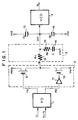
- FIG. 1 A circuit diagram of the first mode of the present invention is shown in Figure 1.
- Charge pump 2 comprises P channel transistor 9, N channel transister 10 and NOT circuit 11.
- LPF 3 comprises register Ra 12, register Rb 13 and capacitor C 14. Further, at the output terminal of LPF 3, capacitor Ca 15 is connected with the voltage Vdd and capacitor Cb is connected with the voltage Vss.
- PD 1 compares the frequencies and phases of the inputted signal fi and the feedback signal f 0 /N. If the frequency of the feedback signal f 0 /N is lower than that of the inputted signal fi or if the phase of f 0 /N is retarded, then, PD 1 outputs a low level pulse signal PU. On the other hand, if the frequency of the feedback signal f 0 /N is greater than that of the inputted signal fi or if the phase of f 0 /N is advanced, then, PD 1 outputs a low level pulse signal PD. The current flows toward the right, when pulse signal PU is low. Accordingly, charge pump 2 charges capacitor 14 in LPF 3 to increase the output voltage Vo1 of LPF 3.
- output voltage Vo1 which is the input voltage to VCO 4 approaches the value expressed in terms of the reciprocals of the capacitances of Ca 15 and Cb 16, ⁇ [(1/Cb)/(1/Ca+1/Cb] ⁇ Vdd ⁇ .
- fr is a freerunning frequency
- K is a conversion gain of VCO 4.
- the output frequency f 0 from VCO 4 varies around the freerunning frequency fr.
- f 0 is proportional to Vo1.
- the input voltage Vo1 which is required to obtain the desired frequency f 0 is specific to VCO 4.
- the voltage Vo1 is controlled by PD 1and charge pump 2.
- the value of Vo2 can be adjusted to be the input voltage value which is required to obtain the desired frequency f 0 .
- FIG. 2 A circuit diagram explaining the second embodiment of the present invention is shown in Figure 2.
- demultiplexer (DEMUX) 18 is connected with NOT circuit 17 which is further connected with analog switch 19.
- DEMUX 18 is connected also with capacitor portions 20a to 20d ( hereinafter referred to as 20x) each of which comprises analog switch and capacitor.
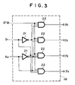
- Figure 3 is a circuit diagram of DEMUX 18.
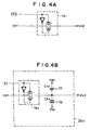
- Figure 4A is a circuit diagram of analog switch 19.
- Figure 4B is a circuit diagram of capacitor portion 20x each of which comprises analog switch and capacitor. In the following, only the differences from the first embodiment of the present invention are explained.
- Signals S 0 and S 1 are control signals which decide the dividing ratio of frequency divider 5 and are inputted into DEMUX 18 as well as frequency divider 5. Further, the signal STB becomes high level, when signal S1 and input signal fi are inputted into PLL circuit or changed in PLL circuit. Signals S 0 , S 1 and STB are inputted into DEMUX 18. When the signal STB becomes low, all the outputs y x from DEMUX 18 becomes low. The electric potential of the signal STB is inverted by NOT circuit 17. Then, the inverted signal of the signal STB turns on analog switch 19 and changes the output voltage Vo1 from LPF 3 into the input voltage Vo2 into VCO 4, without passing through any capacitor portion 20x.
- the inverted signal of the signal STB functions as a bypass signal.
- analog switch is turned off and one of the output signals y 0 to y 3 becomes high on the basis of the values of control signals S 0 and S 1 by DEMUX 18.
- analog switch 19x in capacitor portion 20x is turned on and the output Vo1 from LPF 3 becomes Vo2 which is almost the same as the input voltage which is required to obtain the desired frequency f 0 by virtue of Cax and Cbx, as explained in the first mode of the present invention.
- the dividing ratio be 1/1,1/2,1/3,...
- the output voltage Vo1 from LPF 4 can approach the input voltage which is required to obtain the desired frequency f 0 .
- the deviation of the phase and frequency can be minimized.
- the pull-in time can be reduced, when the input signal frequency fi has been inputted or changed, and when the dividing ratio has been changed.
- the dividing ratio may happen to be unity.
- analog switch 19 when analog switch 19 is connected with VCO 4, the response to the output from PD 1 is improved comparing with the first mode of the present invention, because capacitance portions 20x are separated. Accordingly, the response is maintained, even when the impedances of capacitance portions 20x are fixed to be greater than that of LPF 3.
Landscapes
- Stabilization Of Oscillater, Synchronisation, Frequency Synthesizers (AREA)
Applications Claiming Priority (2)
| Application Number | Priority Date | Filing Date | Title |
|---|---|---|---|
| JP9213216A JP3047968B2 (ja) | 1997-08-07 | 1997-08-07 | Pll回路 |
| JP213216/97 | 1997-08-07 |
Publications (1)
| Publication Number | Publication Date |
|---|---|
| EP0896434A1 true EP0896434A1 (fr) | 1999-02-10 |
Family
ID=16635463
Family Applications (1)
| Application Number | Title | Priority Date | Filing Date |
|---|---|---|---|
| EP98114841A Withdrawn EP0896434A1 (fr) | 1997-08-07 | 1998-08-06 | Circuit de boucle à verrouillage de phase |
Country Status (5)
| Country | Link |
|---|---|
| US (1) | US6084480A (fr) |
| EP (1) | EP0896434A1 (fr) |
| JP (1) | JP3047968B2 (fr) |
| KR (1) | KR100319422B1 (fr) |
| TW (1) | TW418566B (fr) |
Cited By (2)
| Publication number | Priority date | Publication date | Assignee | Title |
|---|---|---|---|---|
| GB2361119A (en) * | 2000-04-07 | 2001-10-10 | Lucent Technologies Inc | Phase locked loop synthesisers |
| FR2855341A1 (fr) * | 2003-05-22 | 2004-11-26 | Eads Telecom | Circuit de commande de decalage en tension pour pll |
Families Citing this family (7)
| Publication number | Priority date | Publication date | Assignee | Title |
|---|---|---|---|---|
| GB2339352B (en) * | 1998-06-30 | 2002-02-06 | Lsi Logic Corp | Testing analog to digital converters |
| JP4407031B2 (ja) * | 2000-09-21 | 2010-02-03 | ソニー株式会社 | 位相同期ループ回路および遅延同期ループ回路 |
| US7304545B1 (en) | 2000-11-30 | 2007-12-04 | Marvell International Ltd. | High latency timing circuit |
| US6732286B1 (en) | 2000-11-30 | 2004-05-04 | Marvell International, Ltd. | High latency timing circuit |
| US6466100B2 (en) | 2001-01-08 | 2002-10-15 | International Business Machines Corporation | Linear voltage controlled oscillator transconductor with gain compensation |
| US7167056B2 (en) * | 2004-09-30 | 2007-01-23 | Texas Instruments Incorporated | High performance analog charge pumped phase locked loop (PLL) architecture with process and temperature compensation in closed loop bandwidth |
| US7782096B2 (en) * | 2007-08-08 | 2010-08-24 | Texas Instruments Incorporated | Track-and-hold circuit with low distortion |
Citations (4)
| Publication number | Priority date | Publication date | Assignee | Title |
|---|---|---|---|---|
| JPS5776931A (en) * | 1980-10-30 | 1982-05-14 | Denki Kogyo Kk | Pll circuit |
| US5021749A (en) * | 1988-05-11 | 1991-06-04 | Seiko Epson Corporation | Switchable capacitor loop filter for phase locked loop |
| EP0482823A2 (fr) * | 1990-10-22 | 1992-04-29 | Nec Corporation | Synthétiseur de fréquence à PLL permettant de changer la fréquence de sortie à une vitesse élevée |
| US5355098A (en) * | 1992-04-24 | 1994-10-11 | Ricoh Company, Ltd. | Phase-locked loop with memory storing control data controlling the oscillation frequency |
Family Cites Families (4)
| Publication number | Priority date | Publication date | Assignee | Title |
|---|---|---|---|---|
| JPS61106064A (ja) * | 1984-10-25 | 1986-05-24 | Yokogawa Hokushin Electric Corp | Dc/dcコンバ−タ |
| JPS62181525A (ja) * | 1986-02-05 | 1987-08-08 | Yokogawa Electric Corp | 信号発生回路 |
| US5335365A (en) * | 1991-07-08 | 1994-08-02 | Motorola, Inc. | Frequency synthesizer with VCO output control |
| JPH0661852A (ja) * | 1992-08-04 | 1994-03-04 | Nec Corp | フェーズロックドループ |
-
1997
- 1997-08-07 JP JP9213216A patent/JP3047968B2/ja not_active Expired - Fee Related
-
1998
- 1998-07-29 US US09/124,761 patent/US6084480A/en not_active Expired - Fee Related
- 1998-07-30 TW TW087112667A patent/TW418566B/zh active
- 1998-08-06 EP EP98114841A patent/EP0896434A1/fr not_active Withdrawn
- 1998-08-06 KR KR1019980032002A patent/KR100319422B1/ko not_active Expired - Fee Related
Patent Citations (4)
| Publication number | Priority date | Publication date | Assignee | Title |
|---|---|---|---|---|
| JPS5776931A (en) * | 1980-10-30 | 1982-05-14 | Denki Kogyo Kk | Pll circuit |
| US5021749A (en) * | 1988-05-11 | 1991-06-04 | Seiko Epson Corporation | Switchable capacitor loop filter for phase locked loop |
| EP0482823A2 (fr) * | 1990-10-22 | 1992-04-29 | Nec Corporation | Synthétiseur de fréquence à PLL permettant de changer la fréquence de sortie à une vitesse élevée |
| US5355098A (en) * | 1992-04-24 | 1994-10-11 | Ricoh Company, Ltd. | Phase-locked loop with memory storing control data controlling the oscillation frequency |
Non-Patent Citations (1)
| Title |
|---|
| PATENT ABSTRACTS OF JAPAN vol. 006, no. 155 (E - 125) 17 August 1982 (1982-08-17) * |
Cited By (4)
| Publication number | Priority date | Publication date | Assignee | Title |
|---|---|---|---|---|
| GB2361119A (en) * | 2000-04-07 | 2001-10-10 | Lucent Technologies Inc | Phase locked loop synthesisers |
| FR2855341A1 (fr) * | 2003-05-22 | 2004-11-26 | Eads Telecom | Circuit de commande de decalage en tension pour pll |
| WO2004105249A3 (fr) * | 2003-05-22 | 2005-01-27 | Eads Telecom | Circuit de commande de decalage de tension pour pll |
| US7764093B2 (en) | 2003-05-22 | 2010-07-27 | Eads Telecom | Voltage shift control circuit for PLL |
Also Published As
| Publication number | Publication date |
|---|---|
| JPH1155114A (ja) | 1999-02-26 |
| KR100319422B1 (ko) | 2002-02-19 |
| KR19990023417A (ko) | 1999-03-25 |
| US6084480A (en) | 2000-07-04 |
| TW418566B (en) | 2001-01-11 |
| JP3047968B2 (ja) | 2000-06-05 |
Similar Documents
| Publication | Publication Date | Title |
|---|---|---|
| US5847617A (en) | Variable-path-length voltage-controlled oscillator circuit | |
| US6229399B1 (en) | Multiple frequency band synthesizer using a single voltage control oscillator | |
| US6320435B1 (en) | PLL circuit which can reduce phase offset without increase in operation voltage | |
| US7339438B2 (en) | Phase and delay locked loops and semiconductor memory device having the same | |
| US6967538B2 (en) | PLL having VCO for dividing frequency | |
| US8508265B2 (en) | Differential controlled phase locked loop circuit | |
| US6255872B1 (en) | Charge pump circuit for PLL | |
| JP3388071B2 (ja) | 位相同期回路、および位相同期回路を含む半導体装置 | |
| EP0945986B1 (fr) | Circuit pompe de charge pour boucle à verrouillage de phase | |
| US6084480A (en) | Phase locked loop circuit including voltage controlled oscillator and low pass filter | |
| US5081429A (en) | Voltage controlled oscillator with controlled load | |
| US4749951A (en) | Low-pass filter circuit with variable time constant | |
| US6614318B1 (en) | Voltage controlled oscillator with jitter correction | |
| US7215209B2 (en) | Controllable idle time current mirror circuit for switching regulators, phase-locked loops, and delay-locked loops | |
| US7023249B1 (en) | Phase locked loop with low phase noise and fast tune time | |
| US6380810B1 (en) | Reduced lock time for a phase locked loop | |
| US20070090882A1 (en) | Phase locked loop filter | |
| US7498886B2 (en) | Clock distribution system and method thereof | |
| US6320458B1 (en) | Integrated structure with an analog unit supplied by an external supply voltage by means of a low-pass filter and driving elements | |
| US6590459B2 (en) | Phase lock circuit | |
| KR920013933A (ko) | Pll 합성회로 | |
| US20090206893A1 (en) | Charge pump circuit and pll circuit | |
| US6546059B1 (en) | Adaptive integrated PLL loop filter | |
| US5163074A (en) | Dynamic frequency divider circuit with capacitor in loop to achieve fifty percent duty cycle output | |
| KR100222673B1 (ko) | 위상고정루프회로 |
Legal Events
| Date | Code | Title | Description |
|---|---|---|---|
| PUAI | Public reference made under article 153(3) epc to a published international application that has entered the european phase |
Free format text: ORIGINAL CODE: 0009012 |
|
| AK | Designated contracting states |
Kind code of ref document: A1 Designated state(s): DE GB |
|
| AX | Request for extension of the european patent |
Free format text: AL;LT;LV;MK;RO;SI |
|
| 17P | Request for examination filed |
Effective date: 19990301 |
|
| AKX | Designation fees paid |
Free format text: DE GB |
|
| 17Q | First examination report despatched |
Effective date: 20020510 |
|
| STAA | Information on the status of an ep patent application or granted ep patent |
Free format text: STATUS: THE APPLICATION HAS BEEN WITHDRAWN |
|
| 18W | Application withdrawn |
Withdrawal date: 20020827 |