EP0896448B1 - Optisches Knotensystem für Ringarchitektur und zugehöriges Verfahren - Google Patents
Optisches Knotensystem für Ringarchitektur und zugehöriges Verfahren Download PDFInfo
- Publication number
- EP0896448B1 EP0896448B1 EP98306016A EP98306016A EP0896448B1 EP 0896448 B1 EP0896448 B1 EP 0896448B1 EP 98306016 A EP98306016 A EP 98306016A EP 98306016 A EP98306016 A EP 98306016A EP 0896448 B1 EP0896448 B1 EP 0896448B1
- Authority
- EP
- European Patent Office
- Prior art keywords
- optical
- wavelength
- optical signal
- incoming
- signal
- Prior art date
- Legal status (The legal status is an assumption and is not a legal conclusion. Google has not performed a legal analysis and makes no representation as to the accuracy of the status listed.)
- Expired - Lifetime
Links
- 230000003287 optical effect Effects 0.000 title claims description 340
- 238000000034 method Methods 0.000 title claims description 10
- 230000003750 conditioning effect Effects 0.000 claims description 20
- 230000005540 biological transmission Effects 0.000 description 15
- 239000013307 optical fiber Substances 0.000 description 8
- 239000000835 fiber Substances 0.000 description 6
- 238000010586 diagram Methods 0.000 description 5
- RYGMFSIKBFXOCR-UHFFFAOYSA-N Copper Chemical compound [Cu] RYGMFSIKBFXOCR-UHFFFAOYSA-N 0.000 description 3
- 229910052802 copper Inorganic materials 0.000 description 3
- 239000010949 copper Substances 0.000 description 3
- 238000004891 communication Methods 0.000 description 2
- 238000013461 design Methods 0.000 description 2
- 238000005516 engineering process Methods 0.000 description 2
- 239000000284 extract Substances 0.000 description 2
- 238000012545 processing Methods 0.000 description 2
- 238000011144 upstream manufacturing Methods 0.000 description 2
- 230000008859 change Effects 0.000 description 1
- 238000006243 chemical reaction Methods 0.000 description 1
- 230000008878 coupling Effects 0.000 description 1
- 238000010168 coupling process Methods 0.000 description 1
- 238000005859 coupling reaction Methods 0.000 description 1
- 230000001419 dependent effect Effects 0.000 description 1
- 238000012423 maintenance Methods 0.000 description 1
- 238000012986 modification Methods 0.000 description 1
- 230000004048 modification Effects 0.000 description 1
- 230000005693 optoelectronics Effects 0.000 description 1
- 230000000737 periodic effect Effects 0.000 description 1
- 230000008569 process Effects 0.000 description 1
- 229910052710 silicon Inorganic materials 0.000 description 1
- 239000010703 silicon Substances 0.000 description 1
- 238000000638 solvent extraction Methods 0.000 description 1
- 230000003595 spectral effect Effects 0.000 description 1
Images


Classifications
-
- H—ELECTRICITY
- H04—ELECTRIC COMMUNICATION TECHNIQUE
- H04J—MULTIPLEX COMMUNICATION
- H04J14/00—Optical multiplex systems
- H04J14/02—Wavelength-division multiplex systems
- H04J14/0201—Add-and-drop multiplexing
-
- H—ELECTRICITY
- H04—ELECTRIC COMMUNICATION TECHNIQUE
- H04J—MULTIPLEX COMMUNICATION
- H04J14/00—Optical multiplex systems
- H04J14/02—Wavelength-division multiplex systems
- H04J14/0201—Add-and-drop multiplexing
- H04J14/0202—Arrangements therefor
- H04J14/0206—Express channels arrangements
-
- H—ELECTRICITY
- H04—ELECTRIC COMMUNICATION TECHNIQUE
- H04J—MULTIPLEX COMMUNICATION
- H04J14/00—Optical multiplex systems
- H04J14/02—Wavelength-division multiplex systems
- H04J14/0201—Add-and-drop multiplexing
- H04J14/0202—Arrangements therefor
- H04J14/0213—Groups of channels or wave bands arrangements
Definitions
- the present invention relates to optical ring architectures in general and, more particularly, to an optical node system for an optical ring architecture.
- a typical central office ring configuration 100 is depicted in Fig. 1 and includes a plurality of central offices 101a-d. Each central office (CO) 101a-d is capable of transmitting calls to any of the other COs, either directly via direct connections 103a-d or indirectly through other COs as shown by logical connections 105a-b.
- a CO 101a includes an add/drop multiplexer (not shown) which adds calls to the ring 103a-d destined for another CO 101b-d or drops calls from the ring 103a-d for the CO 101a.
- Fig. 2 depicts a more detailed diagram of a ring architecture 106 of COs 101a-c.
- each CO 101a-c is capable of receiving and transmitting information over a plurality of optical fibers 107.
- each fiber 107 operates at a predetermined optical wavelength or wavelength band, but a single optical fiber 107 could carry traffic having multiple wavelengths.
- the optical fibers 107 can be unidirectional in either direction or bi-directional. Some of the optical signals on the optical fibers 107 will terminate at the CO 101a-c in that terminal equipment (not shown) in the CO 101a-c converts the optical signal to electronic form, while other optical signals will continue through the ring 106.
- an optical signal on a path 107 for destination equipment 110 is "dropped" from the ring by an add/drop multiplexer (not shown) in the CO 101a to terminal equipment (not shown) in the CO 101a.
- the terminal equipment (not shown) in the CO 101a may convert the optical signal to an electrical signal and pass the electrical signal along path 112 to destination equipment 110.
- the path 112 could be copper lines, and the destination equipment 110 is typically a terminal.
- Source equipment 114 produces a signal along path 116 to the CO 101a.
- the path 116 could be copper lines for carrying electrical signals.
- the terminal equipment receives the electrical signal and converts it to an optical signal.
- the add/drop multiplexer (not shown) in the CO 101a receives the optical signal and adds it onto a path 107.
- the optical signal added is routed along one or more of the paths 107 interconnecting one or more of the other COs 101a-c and is eventually "dropped," for instance, by an add/drop multiplexer (not shown) of the CO 101c which is connected to the destination equipment 118.
- the add/drop multiplexer passes the optical signal to terminal equipment (not shown) in the CO 101c.
- the terminal equipment (not shown) in the CO 101c passes the signal along path 120 to the destination equipment 118.
- Each of the optical signals not being dropped at a particular CO 101a-c can be amplified and passed along to the next CO.
- FIG. 3 shows a more detailed diagram of a CO 130 in a ring architecture.
- a CO 132 transmits over a path 134 a plurality of optical signals as a wavelength division multiplexed optical signal with wavelengths ⁇ l .. ⁇ n .
- WDM wavelength division multiplexing
- the optical signal is received by the CO 130, and a pre-amplifier 138 might be used to amplify the optical signal.
- EDFA erbium-doped fiber amplifier
- an add/drop multiplexer 140 receives the optical signal.
- the add/drop multiplexer 140 includes wavelength selection devices 142 and 144, such as a wavelength grating routers (WGRs).
- WGRs wavelength grating routers
- An example of a WGR is disclosed in " Integrated Optics NxN Multiplexer On Silicon", Dragone et al., IEEE Phot. Technol. Lett., Vol. 3, pages 896-899 (1991 ).
- the WGR 142 routes the incoming optical signals as a function of wavelength, to a particular output port of the WGR 142. For example, an optical signal at a wavelength of ⁇ 1 applied over the path 134 to WGR 142 is routed by the WGR 142 to path 146. Moreover, an optical signal at a wavelength of ⁇ 2 applied over the path 134 to the WGR 142 is routed by the WGR 142 to path 148. Optical signals having particular wavelengths can be "dropped" by the WGR 142. In this particular example, an optical signal having a particular wavelength ⁇ n is routed onto path 150 by the WGR 142 and thereby dropped to terminal equipment 152.
- the terminal equipment 152 includes a receiver 156 that receives the optical signal from the path 150 and converts the optical signal to an electrical signal, thereby terminating the optical path for that particular wavelength.
- the receiver 156 outputs the electrical signal to electrical circuitry 158 for routing the electrical signal to the proper destination equipment 160.
- the electrical circuitry 158 can include a host digital terminal, switches and other electronic processors and circuitry.
- the destination equipment 160 can include subscriber telephones 162a-b, remote terminal equipment 164 connected to subscriber telephones 162c-d, or other local data networks.
- the electrical signal representing the call passes over path 166 to the CO 130.
- the electrical circuitry 158 processes the call and sends the electrical signal to transmitter 170.
- the transmitter 170 outputs an optical signal having the wavelength ⁇ n by using the electrical signal to modulate a laser that can produce light having the wavelength ⁇ n .
- the transmitter 170 transmits the optical signal via path 172 to WGR 144, which multiplexes the optical signal onto the wavelength division multiplexed signal on path 174.
- the optical signal can be amplified by amplifier 176, such as an EDFA, before being output from the CO 130.
- optical fibers corresponding to optical signals dropped at an add/drop multiplexer on the ring terminate at the add/drop multiplexer.
- the optical fiber terminates at the terminal equipment 152 where the optical signal is converted to an electrical signal.
- the transmitter 170 must provide light having wavelength ⁇ n from an optical source.
- a relatively costly and accurately tuned laser and its supporting electronics is used for each wavelength of optical signals dropped at each add/drop node on the ring.
- current ring architectures can be costly and inflexible.
- EP-A-0 668 674 discloses an optical wavelength division multiplex network system.
- the optical multiplex network system is designed to permit communication between any of a plurality of nodes via a main trunk line, constructed by interconnecting nodes using an optical fiber and including a multi-wavelength light source.
- the optical network of Toshiba includes a central node and multiple terminal nodes.
- the terminal nodes include an optical wavelength demultiplexer for demultiplexing optical signals of n-combinations of wavelengths from the main trunk line.
- the Trunk line contains multi-wavelength light from light source.
- An optical signal from the main trunk line is input to the (add-drop multiplexer) ADM filter which filters out signals of wavelength ⁇ k and ⁇ k', which are directed to the optical wavelength division multiplexer (WDM)
- WDM optical wavelength division multiplexer
- a Wavelength divisional multiplexer separates signals ⁇ k and ⁇ k'.
- the optical signal ⁇ k the outgoing signal carrier, is directed to the optical modulator, where the signal is modulated according to a transmission signal, and transmitted to the main Trunk line via the ADM filter.
- Optical signal ⁇ k', containing the incoming signal is directed to the optical receiver.
- the optical receiver converts optical signal ⁇ k' into a reception signal, but does not return the signal back to the Trunk line. Therefore, the optical wavelength of a signal can only be modulated with an outgoing transmission before it is received and dropped from the network.
- EP0541983A1 is directed to an optical local area network system and nodal apparatus used therein.
- a node apparatus in an optical LAN system Upon receiving a data transmission request, a node apparatus in an optical LAN system receives a light of a wavelength assigned to a destination node apparatus. Where the received light is not modulated, the light will be modulated by a transmitting data, and where the received light is modulated, the received light is passed through the transmitting node apparatus without further modulation.
- EP0536041A1 is directed to a system for optical linking of subscriber terminals to a central station of a telecommunications network, the said subscriber terminals each including an optical transmitter and an optical receiver.
- the optical signal transmitted by each of the optical transmitters, on a different optical carrier for each of these transmitters, is selected based on the optical carrier for a specified communication, by means of dynamic assignment of these various optical transmitters to these various optical receivers.
- N.J. Frigo et al "A Wavelength-Division Multiplexed Passive Optical Netwrok with Cost-Shared Components" IEEE Photonics Technology Letters, No. 11, November 1994, New York, US , XP000486198 is directed to a passive optical network based on a wavelength-division multiplexing router, with modulators at the subscriber terminals.
- a wavelength-division multiplexing router upon arriving at a wavelength-division multiplexed router, downstream packets are routed according to wavelength to the appropriate optical network units.
- This router also multiplexes all upstream-signals onto a single fiber to a central office. This central office separates up- and downstream signals by time partitioning, wavelength, subcarrier frequency, and modulation depth among other factors.
- a node configuration is needed for a more flexible ring architecture which reduces costs associated with current ring architectures.
- the present invention relates to an optical node system for an optical ring network that reduces certain costs associated with current ring architectures by using at least a portion of the light from an incoming optical signal to transmit an outgoing optical signal.
- the node includes an add/drop multiplexer which receives optical signals having a plurality of wavelengths.
- the add/drop multiplexer can be configured to output optical signals having certain wavelengths and to route at least one optical signal from the ring of at least one particular wavelength (or wavelength band) to a corresponding optical transceiver.
- the optical transceiver receives the incoming optical signal of the particular wavelength from the add/drop multiplexer and transmits an outgoing optical signal at the particular wavelength with at least a portion of the light from the incoming optical signal.
- the optical transceiver can modulate outgoing information onto the light of the incoming optical signal and/or pass at least a portion of the incoming optical signal with incoming information for transmission as the outgoing optical signal onto the optical ring network.
- the optical node system alleviates the need for nodes to have a laser tuned to the particular wavelength for transmitting an outgoing optical signal at the particular wavelength.
- the optical node system includes an add/drop multiplexer which receives optical signals having a plurality of wavelengths, outputs optical signals having a subset of those wavelengths, and routes at least one optical signal from the ring of at least one particular wavelength (or wavelength band) to an optical transceiver.
- the optical transceiver transmits an outgoing optical signal at the particular wavelength with at least a portion of the light from the incoming optical signal.
- the optical transceiver can suppress incoming information on the incoming optical signal if any and modulate outgoing information onto the light of the incoming optical signal. Additionally, the optical transceiver can pass at least a portion of the incoming optical signal with incoming information for transmission as the outgoing optical signal onto the optical ring network. Furthermore, the optical node system can provide non-terminating (i.e., not completely ending at an electrical path) optical paths for certain wavelengths throughout the ring, thereby reducing the need for optical sources producing light at those wavelengths at the nodes along the ring.
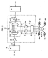
- FIG. 4 shows an optical node/ring configuration 180 according to the principles of the present invention.
- a CO 184 provides optical signals having a plurality of wavelengths ⁇ l ... ⁇ n along optical fiber path 186 to an add/drop node 188.
- the add/drop node 188 is representative of one of a number of nodes that can form the ring 180.
- the node 188 may or may not be part of a CO 190 shown in dashed lines.
- the optical signals on path 186 are amplified by pre-amplifier 192 (optional).
- an optical add/drop multiplexer 194 uses wavelength selection devices, such as WGR 196 to divide the optical signals by wayelength onto paths 200a - 200n, several of which are directed to a WGR 202.
- the add/drop multiplexer 194 also drops one or more of the paths 200 to optical transceiver circuitry 204, which can include one or more optical transceivers corresponding to particular wavelengths (or wavelength bands).
- an optical transceiver 208 receives an incoming optical signal of a particular wavelength (or wavelength bands) from the path 200n. If incoming user information intended for dropping at the node 188 is modulated onto the optical signal, the optical transceiver 208 can retrieve the downstream user information onto the path 214 to terminal equipment 209. The optical transceiver 208 outputs an outgoing optical signal at the particular wavelength onto path 212 to the WGR 202 from at least a portion of the light from the received optical signals. In doing so, the optical transceiver 208 can receive an optical signal at the particular wavelength and modulate upstream user information provided by the terminal equipment 209 on line 210 onto the light of the optical signals for transmission.
- the optical transceiver 208 can also output incoming optical signals bearing information intended for other nodes without modulating upstream user information onto the incoming optical signals. Depending on the particular embodiment, the optical transceiver 208 can modulate the portion of light from incoming optical signals bearing information after the information on the light is suppressed.
- the terminal equipment 209 can include processing circuitry to provide control signals to the optical transceiver circuitry 204 depending on the design and/or the optical signal. For example, incoming user information destined for multiple locations could be treated differently by the optical transceiver, and/or downstream control information could control the receiving of downstream user information and the modulating of outgoing user information by the optical transceiver 208. As such, the optical transceiver 208 may or may not retrieve incoming user information and may or may not modulate outgoing user information onto the optical signal depending on the design and/or the type of information in the optical signal.
- the WGR 202 combines the optical signal of the particular wavelength with the optical signals at the other inputs of WGR 202 to form a WDM signal on path 220.
- An amplifier 222 such as an EDFA, can be used to amplify the optical signals comprising the WDM signal.
- the optical transceiver 208 can be configured in various ways to maintain light of a particular wavelength flowing through the ring without the need for an optical source tuned to the particular wavelength at every node where that wavelength is dropped.
- the optical transceiver accomplishes this by receiving at least one incoming optical signal of at least one particular wavelength and using at least a portion of the light from the incoming optical signal for transmission.
- the optical transceiver can output an outgoing optical signal using the same incoming optical signal or an optical signal of the same wavelength from at least a portion of the light of the incoming optical signal which has been altered and/or modulated with outgoing user information.
- the node according to the principles of the present invention enables a ring architecture with continuous or non-terminating optical paths (i.e., optical paths do not end at an electrical path) of particular wavelengths.
- Such an optical ring architecture resulting from the optical node system provides a cost incentive for using optical local loops or optical distribution systems by reducing the need and costs associated with conventional electrical terminal equipment or optical/electrical conversion equipment.
- An optical local loop system is disclosed in U.S. Patent No. 5,559,624 to Darcie et al.
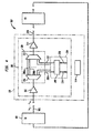
- Fig. 5 shows a block diagram of an embodiment of an optical transceiver 208 for use in a node configuration according to the principles of the present invention.
- an incoming optical signal at a particular wavelength on the path 200n includes information intervals or "blank optical chalkboard" intervals or portions, the light of which is used as a carrier for outgoing information.
- the blank optical chalkboard refers to an incoming optical signal with no incoming information.
- the optical transceiver 208 receives the incoming optical signal, and during the data or incoming information intervals of the incoming optical signal, the coupler/modulator 230 couples the incoming optical signals to a receiver 232.
- the receiver 232 receives the incoming optical signals and extracts modulated data from the optical signals where there is incoming information to be dropped. In one particular embodiment, the receiver 232 converts the modulated data into electrical data signals which are provided to the terminal equipment 209. In such an embodiment, the receiver 232 can employ any well known type of optical receiver capable of receiving the optical signal from path 200n and converting it to an electrical signal.
- the coupler/modulator 230 can also route the incoming signal towards the path 212.
- the coupler/modulator 230 modulates outgoing user information from the terminal equipment 209 onto the light of the incoming optical signal according to signal and control circuitry 234.
- the coupler/modulator 230 obtains optical signals having a particular wavelength and modulates outgoing information onto at least a portion of the light from the incoming optical signals for transmission as outgoing optical signals onto the path 212.
- the coupler/modulator 230 routes all of the incoming optical signals to the receiver 232 during the data interval of the optical signal as controlled by the signal and control circuitry 234.
- the coupler/modulator 230 routes all of the incoming optical signals towards the path 212, and the coupler/modulator 230 modulates outgoing information onto the optical signal for transmission onto the path 212.
- the signal and control circuitry 234 receives information from the terminal equipment 209 as to when the incoming optical signal includes incoming data or information to be dropped and when the optical signal includes the optical chalkboard for modulation of outgoing information, which could be identical to the incoming user information.
- FIG. 6 shows another version of the optical transceiver 208.
- the coupler/modulator 230 includes a coupler 240.
- the coupler 240 routes at least a portion of the downstream optical signal (for example, 10%) to the receiver 232 and the remaining portion (for example, 90%) is coupled on a path 250 to a modulator 244.
- the receiver 232 extracts the incoming information from the portion of the incoming optical signal which is coupled onto the path 245 by the coupler 240.
- the remaining portion of the optical signal can be either passed on to the path 212 without modulation, or if the transmission of outgoing information is desired, the modulator 244 modulates the remaining portion of the incoming optical signal with the outgoing information to form the outgoing optical signal.
- the outgoing optical signal can be amplified with optional amplifier 222 ( FIG. 4 ) if necessary.
- this embodiment enables incoming data to be obtained by the receiver 232 while providing an optical signal at a particular wavelength for modulation and/or transmission without delay. If the incoming optical signal is to be forwarded to other destinations, the signal and control circuitry 234 can provide control signals to the modulator 244 and to signal conditioning circuitry 248 so that the incoming optical signal is not altered. As such, the incoming optical signal can continue flowing on the ring without interruption. In certain embodiments, if at least a portion of the incoming optical signal which has been modulated with incoming user information on the path 250 is to be used for modulation and transmission of outgoing user information, the signal and control circuitry 234 provides control signals to the signal conditioning circuitry 248.
- the signal conditioning circuitry 248 effectively counteracts, removes, suppresses and/or attenuates the modulated portion of the incoming optical signal.
- the signal conditioning circuit 248 includes a series of optical amplifiers (not shown) operating in saturation as will be discussed below.
- the signal conditioning circuitry 248 outputs a relatively unmodulated optical signal of the particular wavelength on the path 250 to the modulator 244.
- the optical transceiver 208 can determine the presence of a blank optical chalkboard interval by receiving incoming information to signal the start of the blank optical chalkboard.
- the modulator 244 modulates the optical signal on the path 250 with outgoing user information as provided and controlled by the signal and control circuitry 234. In this description, modulation can include gain.
- the modulator 244 can include a LiNbO, modulator manufactured by Lucent Technologies, Inc., Murray Hill, N. J., for example.
- the modulator 244 transmits the outgoing modulated optical signals along the path 212 at the appropriate wavelength for the WGR 202 ( FIG. 4 ) to be combined with the other optical signals on the path 220 ( FIG. 4 ).
- the signal conditioning circuitry 248 can be used to suppress the modulated portion of the incoming optical signal.
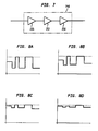
- FIG. 7 shows an embodiment of signal conditioning circuitry 248.
- the signal conditioning circuitry 248 includes a plurality of optical signal amplifier circuits 255, 257 and 259 connected in series.
- the amplifier circuits 255, 257 and 259 can operate in their saturation range. When operating in the saturation range, each amplifier stage of the signal conditioning circuit 248 attenuates the modulated portion of the incoming optical signal.
- feed forward techniques could be used to control the gains of the amplifier circuits 255, 257 and 259. Such techniques may require that some level of light be present at all time (i.e. contrast ratio ⁇ 1).
- FIGs.8a-8d show how one embodiment of the signal conditioning circuitry 248 suppresses the modulated portion of the incoming optical signal at each amplifier stage.
- FIG. 8a shows the incoming optical signal modulated with incoming information at the input to the signal conditioning circuitry 248.
- FIG. 8b shows the incoming optical signal being suppressed after passing through the amplifier circuit 255, and
- FIG. 8c shows the incoming optical signal being further suppressed after passing through the amplifier circuit 257.
- FIG. 8d shows the incoming optical signal after passing through the amplifier circuit 259.
- the optical signal can be passed through more or fewer optical amplifiers, as necessary, to remove as much of the modulated portion of the signal as desired.
- the signal conditioning circuitry 248 can be configured so that control signals can enable/disable the signal conditioning circuitry 248 or change the operation of the amplifier circuits 255, 257 and 259.
- the amplifier circuits could be designed to operate in saturation or not.
- the present invention provides a system that obviates the need for providing individual laser light sources for each wavelength dropped or routed within each node to the optical transceiver according to the principles of the present invention, thus simplifying the structure, reducing overall cost and reducing the amount of maintenance of the entire ring architecture.
- the periodic properties of the WGR can be used to allow light of additional wavelengths spaced by multiples of the free spectral range (FSR) to be used without additional optical circuitry, thereby providing flexibility and the potential for increased capacity.
- FSR free spectral range
- a WGR could route optical signals having wavelengths of ⁇ 1 and ⁇ n+1 together as well as ⁇ 2 and ⁇ n+2 together and so on.
- the node configuration according to the principles of the present invention can quite efficiently accommodate optical distribution systems, thereby further reducing costs by alleviating the need for electrical terminal equipment.
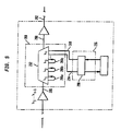
- FIG. 9 shows an alternative embodiment for the optical node system which uses a different configuration for the optical add/drop multiplexer 280 than was used for the add/drop multiplexer 194 ( FIG. 4 ).
- the add/drop multiplexer 280 includes a single wavelength selection device, such as a 2 X 2n WGR 282 which is shown having twice as many output ports when compared to a previous WGR described above.
- the WGR 282 receives optical signals having a plurality of wavelengths ⁇ 1 .. ⁇ n from the line 286.
- optical signals having certain wavelengths ⁇ 1 .. ⁇ 3 are output onto line 290 for transmission onto the ring 292.
- incoming optical signals having a wavelength ⁇ n are routed over line 294 to optical transceiver circuitry 296 which includes optical transceiver 298.
- the optical transceiver 298 uses at least a portion of the light from the incoming optical signal to output an outgoing optical signal having the wavelength ⁇ n onto line 300 to the WGR 282.
- the WGR 282 outputs the outgoing optical signal onto line 290 for transmission over the ring 292.
- optical ring network architecture of the central offices described above which employs the optical node system according to the principles of the present invention is merely illustrative, and the node configuration can be used in other optical ring architectures. Additionally, the node configuration according to the principles of the present invention can be implemented utilizing various combinations of application specific, optical and opto-electronic integrated circuits, software driven processing circuitry, or other arrangements of discrete components. What has been described is merely illustrative of the application of the principles of the present invention. Those skilled in the art will readily recognize that these and various other modifications, arrangements and methods can be made to the present invention without strictly following the exemplary applications illustrated and described herein and without departing from the scope of the present invention as set in the appended claims.
Landscapes
- Engineering & Computer Science (AREA)
- Computer Networks & Wireless Communication (AREA)
- Signal Processing (AREA)
- Optical Communication System (AREA)
- Use Of Switch Circuits For Exchanges And Methods Of Control Of Multiplex Exchanges (AREA)
- Small-Scale Networks (AREA)
Claims (10)
- Optisches Ringnetzwerk (180), bestehend aus einer Mehrzahl von optischen Knoten (184 und 190) für die Übermittlung von optischen Signalen entlang des besagten optischen Ringnetzwerks, wobei das besagte Netzwerk umfasst: Einen ersten Knoten (184) mit einem ersten optischen Add/Drop-Multiplexer (194), welcher für den Empfang von optischen Signalen (λ1... λn), die mindestens eine erste Wellenlänge aufweisen, konfiguriert ist, wobei der besagte optische Add/Drop-Multiplexer weiterhin dafür konfiguriert ist, optische Signale (λ1... λn), die mindestens die besagte erste Wellenlänge aufweisen, entlang des besagten optischen Ringnetzwerks an mindestens einen zweiten Knoten (190) auszugeben und mindestens ein eingehendes optisches Signal, dessen besagte erste Wellenlänge mit eingehenden Benutzerinformationen moduliert ist, an einen ersten optischen Transceiver (208) zu routen; und wobei der besagte optische Transceiver an den besagten ersten optischen Add/Drop-Multiplexer gekoppelt und dafür konfiguriert ist, das besagte mindestens eine eingehende optische Signal, welches die besagte erste Wellenlänge aufweist, zu empfangen und mindestens einen Teil des Lichtes des besagten eingehenden optischen Signals, welches die besagte erste Wellenlänge aufweist, auszugeben, um ein ausgehendes optisches Signal mit einer ersten Wellenlänge bereitzustellen;
einen zweiten Knoten (190) mit einem zweiten optischen Add/Drop-Multiplexer (194), welcher für den Empfang mindestens des besagten ausgehenden optischen Signals mit der besagten ersten Wellenlänge von dem besagten ersten Knoten und für das Routen mindestens des besagten empfangenen ausgehenden optischen Signals mit der besagten ersten Wellenlänge an einen zweiten optischen Transceiver (208) ausgelegt ist, wobei der besagte zweite optische Transceiver an den besagten zweiten optischen Add/Drop-Multiplexer gekoppelt und dafür konfiguriert ist, mindestens das besagte empfangene ausgehende optische Signal, welches die besagte erste Wellenlänge aufweist, zu empfangen und mindestens einen Teil des Lichtes des besagten empfangenen ausgehenden optischen Signals mit der besagten ersten Wellenlänge an den besagten zweiten optischen Add/Drop-Multiplexer auszugeben, um ein zweites ausgehendes optisches Signal mit der besagten ersten Wellenlänge entlang des besagten optischen Ringnetzwerks bereitzustellen; und wobei
der besagte erste und der besagte zweite optische Transceiver jeweils ausgehende Benutzerinformationen auf mindestens einen Teil des Lichtes des besagten eingehenden optischen Signals, welches die besagte erste Wellenlänge aufweist, und auf das besagte ausgehende optische Signal, welches die besagte erste Wellenlänge aufweist, modulieren; und
der besagte erste und der besagte zweite optische Transceiver jeweils eine Signalaufbereitungsschaltung (248) umfassen, welche für den Empfang des besagten eingehenden optischen Signals mit der besagten ersten Wellenlänge und des besagten ausgehenden optischen Signals mit der besagten ersten Wellenlänge, die mit eingehenden Benutzerinformationen moduliert worden sind, und für die Entnahme der besagten auf den besagten mindestens einen Teil des Lichtes modulierten eingehenden Benutzerinformationen aus dem besagten eingehenden optischen Signal, welches die besagte ersten Wellenlänge aufweist, und aus dem besagten ausgehenden optischen Signal, welches die besagte erste Wellenlänge aufweist, konfiguriert sind. - Optisches Ringnetzwerk nach Anspruch 1, wobei der besagte optische Add/Drop-Multiplexer eine erste Wellenlängenselektionsvorrichtung (196) umfasst, welche an eine zweite Wellenlängenselektionsvorrichtung (202) gekoppelt und für den Empfang der besagten optischen Signale (λ1... λn), welche mindestens die besagte erste Wellenlänge aufweisen, und des besagten ausgehenden optischen Signals, welches die besagte erste Wellenlänge aufweist, sowie für das Kombinieren der besagten optischen Signale (λ1... λn), welche mindestens die besagte erste Wellenlänge aufweisen, und des besagten ausgehenden optischen Signals, welches die besagte erste Wellenlänge aufweist, von dem besagten ersten optischen Transceiver auf einen optischen Ausgangspfad (220) konfiguriert ist.
- Optisches Ringnetzwerk nach Anspruch 3, wobei die besagte erste und die besagte zweite Wellenlängenselektionsvorrichtung auf derselben physischen Vorrichtung (188) angeordnet sind.
- Optisches Ringnetzwerk nach Anspruch 1, wobei der besagte erste optische Transceiver dafür konfiguriert ist, den besagten mindestens einen Teil des Lichtes aus dem besagten eingehenden optischen Signal, welches die besagte erste Wellenlänge aufweist, mit ausgehenden Benutzerinformationen zu modulieren (244), nachdem eingehende Benutzerinformationen durch die besagte Signalaufbereitungsschaltung aus dem besagten eingehenden optischen Signal, welches die besagte erste Wellenlänge aufweist, entnommen worden sind.
- Optisches Ringnetzwerk nach Anspruch 1, wobei die besagte Signalaufbereitungsschaltung (248) einen modulierten Teil aus dem eingehenden optischen Signal, welches die besagte erste Wellenlänge aufweist und mit eingehenden Benutzerinformationen moduliert ist, entnimmt.
- Optisches Ringnetzwerk nach Anspruch 1, wobei die besagte Signalaufbereitungsschaltung mindestens einen optischen Verstärker (255), (257) und (259) umfasst.
- Optisches Ringnetzwerk nach Anspruch 6, wobei der besagte mindestens eine optische Verstärker in Sättigungszustand arbeitet.
- Verfahren zum Übermitteln von optischen Signalen in einem optischen Ringnetzwerk (180), welches aus mindestens zwei Knoten (184 und 190) besteht, wobei das Verfahren durch die folgenden Schritte gekennzeichnet ist:Empfangen, an einem ersten Knoten (184), von optischen Signalen (λ1... λn), die eine erste Wellenlänge aufweisen, von dem besagten optischen Ringnetzwerk;Routen mindestens eines eingehenden optischen Signals, dessen besagte mindestens erste Wellenlänge mit eingehenden Benutzerinformationen moduliert ist, an einen ersten optischen Transceiver (208); undAusgeben, durch den besagten ersten optischen Transceiver, mindestens eines Teils des Lichtes aus dem besagten eingehenden optischen Signal, welches die besagte mindestens erste Wellenlänge aufweist, um ein ausgehendes optisches Signal mit der besagten ersten Wellenlänge für die Übermittlung an mindestens einen zweiten Knoten auf dem besagten optischen Ringnetzwerk bereitzustellen;Ausgeben, durch den besagten ersten Knoten, des besagten ausgehenden optischen Signals, welches die besagte erste Wellenlänge aufweist, an einen zweiten Knoten (190);Empfangen, an dem zweiten Knoten (190), mindestens des besagten ausgehenden optischen Signals mit der besagten ersten Wellenlänge von dem besagten ersten Knoten;Routen mindestens des besagten empfangenen ausgehenden optischen Signals mit der besagten ersten Wellenlänge an einen zweiten optischen Transceiver (208);Bereitstellen, durch den besagten zweiten optischen Transceiver, mindestens eines Teils des Lichtes aus dem besagten empfangenen ausgehenden optischen Signal, welches die besagte erste Wellenlänge aufweist, als ein zweites ausgehendes optisches Signal mit der besagten ersten Wellenlänge für die Übermittlung auf dem besagten optischen Ringnetzwerk;Ausgeben, durch den besagten zweiten Knoten (190), des besagten zweiten optischen Signals mit der besagten ersten Wellenlänge entlang des besagten optischen Ringnetzwerks;Modulieren, an dem besagten ersten Knoten (184), von ausgehenden Benutzerinformationen auf mindestens einen Teil des Lichtes des besagten eingehenden optischen Signals, welches die besagte erste Wellenlänge aufweist;Empfangen, von dem besagten ersten Knoten (184), des besagten eingehenden optischen Signals, dessen besagte erste Wellenlänge mit den besagten eingehenden Benutzerinformationen moduliert worden ist, an dem besagten zweiten Knoten (190); undEntnehmen, an dem besagten zweiten optischen Transceiver (208), der besagten eingehenden Benutzerinformationen aus dem besagten eingehenden optischen Signal, welches die besagte erste Wellenlänge aufweist.
- Verfahren nach Anspruch 8, weiterhin umfassend:Modulieren des besagten eingehenden optischen Signals, welches die besagte erste Wellenlänge aufweist und aus welchem die eingehenden Benutzerinformationen durch die Signalaufbereitungsschaltung (248) entfernt worden sind, mit den besagten ausgehenden Benutzerinformationen.
- Verfahren nach Anspruch 8, weiterhin den folgenden Schritt umfassend:Kombinieren der besagten optischen Signale (λ1... λn), welche die besagte erste Wellenlänge aufweisen, und des besagten ausgehenden optischen Signals, welches die besagte erste Wellenlänge aufweist, von dem besagten ersten optischen Transceiver auf einen optischen Ausgangspfad (220).
Applications Claiming Priority (2)
| Application Number | Priority Date | Filing Date | Title |
|---|---|---|---|
| US905879 | 1997-08-04 | ||
| US08/905,879 US6222654B1 (en) | 1997-08-04 | 1997-08-04 | Optical node system for a ring architecture and method thereof |
Publications (3)
| Publication Number | Publication Date |
|---|---|
| EP0896448A2 EP0896448A2 (de) | 1999-02-10 |
| EP0896448A3 EP0896448A3 (de) | 2005-01-19 |
| EP0896448B1 true EP0896448B1 (de) | 2012-05-09 |
Family
ID=25421623
Family Applications (1)
| Application Number | Title | Priority Date | Filing Date |
|---|---|---|---|
| EP98306016A Expired - Lifetime EP0896448B1 (de) | 1997-08-04 | 1998-07-28 | Optisches Knotensystem für Ringarchitektur und zugehöriges Verfahren |
Country Status (5)
| Country | Link |
|---|---|
| US (2) | US6222654B1 (de) |
| EP (1) | EP0896448B1 (de) |
| JP (2) | JP4094134B2 (de) |
| KR (1) | KR19990023260A (de) |
| CA (1) | CA2244385C (de) |
Families Citing this family (71)
| Publication number | Priority date | Publication date | Assignee | Title |
|---|---|---|---|---|
| US6222654B1 (en) * | 1997-08-04 | 2001-04-24 | Lucent Technologies, Inc. | Optical node system for a ring architecture and method thereof |
| JPH11275028A (ja) * | 1998-03-20 | 1999-10-08 | Fujitsu Ltd | 光通信システム |
| US6694098B1 (en) * | 1999-12-13 | 2004-02-17 | Nortel Networks Limited | Apparatus and method for reading data from an optical packet header |
| US6735394B1 (en) | 1999-12-15 | 2004-05-11 | Tellabs Operations, Inc. | Per-channel optical amplification using saturation mode |
| US6693033B2 (en) | 2000-02-10 | 2004-02-17 | Motorola, Inc. | Method of removing an amorphous oxide from a monocrystalline surface |
| US6392257B1 (en) | 2000-02-10 | 2002-05-21 | Motorola Inc. | Semiconductor structure, semiconductor device, communicating device, integrated circuit, and process for fabricating the same |
| DE60106736T2 (de) * | 2000-03-31 | 2005-11-24 | At & T Corp. | Weichenanordnung mit wellenleitergitter und mehreren eingängen für broadcast- und multicastdienste |
| US7120359B2 (en) * | 2000-05-22 | 2006-10-10 | Opvista Incorporated | Broadcast and select all optical network |
| US7499647B2 (en) * | 2000-05-22 | 2009-03-03 | Opvista Incorporated | Fully protected broadcast and select all optical network |
| KR20030011083A (ko) | 2000-05-31 | 2003-02-06 | 모토로라 인코포레이티드 | 반도체 디바이스 및 이를 제조하기 위한 방법 |
| US6410941B1 (en) | 2000-06-30 | 2002-06-25 | Motorola, Inc. | Reconfigurable systems using hybrid integrated circuits with optical ports |
| US6501973B1 (en) | 2000-06-30 | 2002-12-31 | Motorola, Inc. | Apparatus and method for measuring selected physical condition of an animate subject |
| US6477285B1 (en) | 2000-06-30 | 2002-11-05 | Motorola, Inc. | Integrated circuits with optical signal propagation |
| US6427066B1 (en) | 2000-06-30 | 2002-07-30 | Motorola, Inc. | Apparatus and method for effecting communications among a plurality of remote stations |
| US7158722B1 (en) | 2000-07-13 | 2007-01-02 | At&T Corp. | Method for operating transparent node for WDM shared “virtual ring” networks |
| US7006767B1 (en) * | 2000-07-13 | 2006-02-28 | At&T Corp. | System for transparent node for WDM shared “virtual ring” networks |
| US6555946B1 (en) | 2000-07-24 | 2003-04-29 | Motorola, Inc. | Acoustic wave device and process for forming the same |
| AU2001277001A1 (en) | 2000-07-24 | 2002-02-05 | Motorola, Inc. | Heterojunction tunneling diodes and process for fabricating same |
| US6788899B2 (en) * | 2000-09-11 | 2004-09-07 | Winston I. Way | Dynamic wavelength add/drop multiplexer for UDWDM optical communication system |
| US7024112B2 (en) * | 2000-09-11 | 2006-04-04 | Opvista Incorporated | In-band wavelength conversion wavelength buffering and multi-protocol lambda switching |
| US6638838B1 (en) | 2000-10-02 | 2003-10-28 | Motorola, Inc. | Semiconductor structure including a partially annealed layer and method of forming the same |
| US6563118B2 (en) | 2000-12-08 | 2003-05-13 | Motorola, Inc. | Pyroelectric device on a monocrystalline semiconductor substrate and process for fabricating same |
| US20020096683A1 (en) | 2001-01-19 | 2002-07-25 | Motorola, Inc. | Structure and method for fabricating GaN devices utilizing the formation of a compliant substrate |
| US6673646B2 (en) | 2001-02-28 | 2004-01-06 | Motorola, Inc. | Growth of compound semiconductor structures on patterned oxide films and process for fabricating same |
| US7027733B2 (en) * | 2001-03-19 | 2006-04-11 | At&T Corp. | Delivering multicast services on a wavelength division multiplexed network using a configurable four-port wavelength selective crossbar switch |
| WO2002082551A1 (en) | 2001-04-02 | 2002-10-17 | Motorola, Inc. | A semiconductor structure exhibiting reduced leakage current |
| US6709989B2 (en) | 2001-06-21 | 2004-03-23 | Motorola, Inc. | Method for fabricating a semiconductor structure including a metal oxide interface with silicon |
| US7769290B2 (en) * | 2001-06-25 | 2010-08-03 | Broadwing Corporation | Optical transmission systems, devices, and methods |
| US6992321B2 (en) | 2001-07-13 | 2006-01-31 | Motorola, Inc. | Structure and method for fabricating semiconductor structures and devices utilizing piezoelectric materials |
| US6646293B2 (en) | 2001-07-18 | 2003-11-11 | Motorola, Inc. | Structure for fabricating high electron mobility transistors utilizing the formation of complaint substrates |
| US7019332B2 (en) | 2001-07-20 | 2006-03-28 | Freescale Semiconductor, Inc. | Fabrication of a wavelength locker within a semiconductor structure |
| US6693298B2 (en) | 2001-07-20 | 2004-02-17 | Motorola, Inc. | Structure and method for fabricating epitaxial semiconductor on insulator (SOI) structures and devices utilizing the formation of a compliant substrate for materials used to form same |
| US6472694B1 (en) | 2001-07-23 | 2002-10-29 | Motorola, Inc. | Microprocessor structure having a compound semiconductor layer |
| US6855992B2 (en) | 2001-07-24 | 2005-02-15 | Motorola Inc. | Structure and method for fabricating configurable transistor devices utilizing the formation of a compliant substrate for materials used to form the same |
| US6585424B2 (en) | 2001-07-25 | 2003-07-01 | Motorola, Inc. | Structure and method for fabricating an electro-rheological lens |
| US6594414B2 (en) | 2001-07-25 | 2003-07-15 | Motorola, Inc. | Structure and method of fabrication for an optical switch |
| US6667196B2 (en) | 2001-07-25 | 2003-12-23 | Motorola, Inc. | Method for real-time monitoring and controlling perovskite oxide film growth and semiconductor structure formed using the method |
| US6462360B1 (en) | 2001-08-06 | 2002-10-08 | Motorola, Inc. | Integrated gallium arsenide communications systems |
| US6589856B2 (en) | 2001-08-06 | 2003-07-08 | Motorola, Inc. | Method and apparatus for controlling anti-phase domains in semiconductor structures and devices |
| US6639249B2 (en) | 2001-08-06 | 2003-10-28 | Motorola, Inc. | Structure and method for fabrication for a solid-state lighting device |
| US20030034491A1 (en) | 2001-08-14 | 2003-02-20 | Motorola, Inc. | Structure and method for fabricating semiconductor structures and devices for detecting an object |
| US6673667B2 (en) | 2001-08-15 | 2004-01-06 | Motorola, Inc. | Method for manufacturing a substantially integral monolithic apparatus including a plurality of semiconductor materials |
| US20030071327A1 (en) | 2001-10-17 | 2003-04-17 | Motorola, Inc. | Method and apparatus utilizing monocrystalline insulator |
| US7231148B2 (en) * | 2002-03-28 | 2007-06-12 | Fujitsu Limited | Flexible open ring optical network and method |
| US7076163B2 (en) | 2002-03-27 | 2006-07-11 | Fujitsu Limited | Method and system for testing during operation of an open ring optical network |
| US7116905B2 (en) | 2002-03-27 | 2006-10-03 | Fujitsu Limited | Method and system for control signaling in an open ring optical network |
| US6916717B2 (en) | 2002-05-03 | 2005-07-12 | Motorola, Inc. | Method for growing a monocrystalline oxide layer and for fabricating a semiconductor device on a monocrystalline substrate |
| US6842562B2 (en) * | 2002-05-30 | 2005-01-11 | Fujitsu Network Communications, Inc. | Optical add/drop node and method |
| US6922529B2 (en) * | 2002-08-09 | 2005-07-26 | Corvis Corporation | Optical communications systems, devices, and methods |
| US7169619B2 (en) | 2002-11-19 | 2007-01-30 | Freescale Semiconductor, Inc. | Method for fabricating semiconductor structures on vicinal substrates using a low temperature, low pressure, alkaline earth metal-rich process |
| US6885065B2 (en) | 2002-11-20 | 2005-04-26 | Freescale Semiconductor, Inc. | Ferromagnetic semiconductor structure and method for forming the same |
| US7020374B2 (en) | 2003-02-03 | 2006-03-28 | Freescale Semiconductor, Inc. | Optical waveguide structure and method for fabricating the same |
| US6965128B2 (en) | 2003-02-03 | 2005-11-15 | Freescale Semiconductor, Inc. | Structure and method for fabricating semiconductor microresonator devices |
| US7116860B1 (en) | 2003-12-05 | 2006-10-03 | Cisco Technology, Inc. | Coupler add/drop node WDM network architecture with periodic cleanup |
| US7577367B2 (en) * | 2004-06-15 | 2009-08-18 | Op Vista Incorporated | Optical communication using duobinary modulation |
| US7450851B2 (en) * | 2004-08-27 | 2008-11-11 | Fujitsu Limited | System and method for modularly scalable architecture for optical networks |
| JP4668658B2 (ja) * | 2005-03-28 | 2011-04-13 | 富士通株式会社 | 波長分割多重伝送装置 |
| JP4709567B2 (ja) * | 2005-03-31 | 2011-06-22 | 富士通株式会社 | ドロップ・アンド・コンティニュー装置 |
| US20060275035A1 (en) * | 2005-05-02 | 2006-12-07 | Way Winston I | Multiple interconnected broadcast and select optical ring networks with revertible protection switch |
| US8139476B2 (en) * | 2005-10-13 | 2012-03-20 | Vello Systems, Inc. | Optical ring networks using circulating optical probe in protection switching with automatic reversion |
| US7720377B2 (en) * | 2006-01-23 | 2010-05-18 | Hewlett-Packard Development Company, L.P. | Compute clusters employing photonic interconnections for transmitting optical signals between compute cluster nodes |
| US7773883B1 (en) | 2007-05-04 | 2010-08-10 | Vello Systems, Inc. | Single-fiber optical ring networks based on optical double sideband modulation |
| WO2009012409A2 (en) | 2007-07-17 | 2009-01-22 | Opvista Incorporated | Optical ring networks having node-to-node optical communication channels for carrying data traffic |
| US8064766B2 (en) * | 2007-10-08 | 2011-11-22 | Nec Laboratories America, Inc. | Orthogonal frequency division multiple access based optical ring network |
| WO2011005540A1 (en) | 2009-06-22 | 2011-01-13 | Burnham Institute For Medical Research | Methods and compositions using peptides and proteins with c-terminal elements |
| JP5301375B2 (ja) * | 2009-07-03 | 2013-09-25 | 日本電信電話株式会社 | 光伝送装置、光伝送システムおよび光伝送方法 |
| US9485050B2 (en) | 2009-12-08 | 2016-11-01 | Treq Labs, Inc. | Subchannel photonic routing, switching and protection with simplified upgrades of WDM optical networks |
| US8705741B2 (en) * | 2010-02-22 | 2014-04-22 | Vello Systems, Inc. | Subchannel security at the optical layer |
| US8542999B2 (en) | 2011-02-01 | 2013-09-24 | Vello Systems, Inc. | Minimizing bandwidth narrowing penalties in a wavelength selective switch optical network |
| GB2503497A (en) * | 2012-06-29 | 2014-01-01 | Oclaro Technology Ltd | Determining a parameter of an optical fibre using a pump light source of an amplifier |
| US20170346445A1 (en) * | 2016-05-31 | 2017-11-30 | Futurewei Technologies, Inc. | Dense Wavelength-Division Multiplexing (DWDM) Network and Method |
Family Cites Families (20)
| Publication number | Priority date | Publication date | Assignee | Title |
|---|---|---|---|---|
| US5058101A (en) * | 1988-12-15 | 1991-10-15 | Bell Communications Research, Inc. | Coherent detection loop distribution system |
| EP0452895B1 (de) * | 1990-04-18 | 1996-07-03 | Canon Kabushiki Kaisha | Optisches Übertragungsnetzwerk und Übertragungsverfahren für dasselbe |
| US5327276A (en) * | 1991-10-15 | 1994-07-05 | Nec Corporation | Optical local area network system and node apparatus used in the same |
| JP3320452B2 (ja) * | 1992-07-15 | 2002-09-03 | 沖電気工業株式会社 | 光中継器の監視制御方式 |
| JP2826441B2 (ja) * | 1993-06-03 | 1998-11-18 | 日本電気株式会社 | 光ネットワーク端末および光ネットワーク |
| EP0615358B1 (de) | 1993-03-11 | 2004-10-20 | AT&T Corp. | Optisches Netzwerk mit Endgerätfernabfrage und optische Netzwerkeinheit dafür, dass Wellenlängen transformiert |
| US5815295A (en) * | 1993-03-11 | 1998-09-29 | Lucent Technologies Inc. | Optical communication system with improved maintenance capabilities |
| US5436750A (en) * | 1993-05-07 | 1995-07-25 | Nec Corporation | Optical repeatered transmission with fault locating capability |
| US5434937A (en) * | 1993-11-16 | 1995-07-18 | At&T Corp. | Optical filter having integrated transceivers |
| JP2551371B2 (ja) * | 1993-12-01 | 1996-11-06 | 日本電気株式会社 | 光中継器 |
| KR960004720B1 (ko) * | 1993-12-10 | 1996-04-12 | 재단법인한국전자통신연구소 | 고장 감내형광 링 통신망(A fault-tolerant optical ring network) |
| US5774244A (en) * | 1994-01-18 | 1998-06-30 | British Telecommunications Public Limited Company | Optical communications networks |
| JP3288859B2 (ja) * | 1994-06-24 | 2002-06-04 | 株式会社東芝 | 光波長多重ネットワークシステム |
| EP1304819B1 (de) * | 1994-02-17 | 2005-08-03 | Kabushiki Kaisha Toshiba | Zentrale Quelle von mehreren Wellenlängen |
| US5488500A (en) * | 1994-08-31 | 1996-01-30 | At&T Corp. | Tunable add drop optical filtering method and apparatus |
| KR0146645B1 (ko) * | 1994-12-19 | 1998-08-17 | 양승택 | 광선로 이중링에서의 장애복구장치 |
| FR2736777B1 (fr) * | 1995-07-12 | 1997-08-08 | Alcatel Nv | Reseau de transmission optique avec multiplexage de longueurs d'onde |
| JPH09321701A (ja) * | 1996-05-31 | 1997-12-12 | Fujitsu Ltd | 光通信システム及び光増幅器 |
| US6222654B1 (en) * | 1997-08-04 | 2001-04-24 | Lucent Technologies, Inc. | Optical node system for a ring architecture and method thereof |
| US6147785A (en) * | 1998-01-28 | 2000-11-14 | Ciena Corporation | Coherent crosstalk attenuation apparatus |
-
1997
- 1997-08-04 US US08/905,879 patent/US6222654B1/en not_active Expired - Lifetime
-
1998
- 1998-07-27 CA CA002244385A patent/CA2244385C/en not_active Expired - Fee Related
- 1998-07-28 EP EP98306016A patent/EP0896448B1/de not_active Expired - Lifetime
- 1998-07-31 KR KR1019980030992A patent/KR19990023260A/ko not_active Ceased
- 1998-08-04 JP JP22070198A patent/JP4094134B2/ja not_active Expired - Lifetime
-
2001
- 2001-01-02 US US09/752,916 patent/US6307654B2/en not_active Expired - Lifetime
-
2007
- 2007-06-18 JP JP2007160416A patent/JP2007306594A/ja active Pending
Also Published As
| Publication number | Publication date |
|---|---|
| JPH11178019A (ja) | 1999-07-02 |
| KR19990023260A (ko) | 1999-03-25 |
| CA2244385C (en) | 2002-07-02 |
| EP0896448A2 (de) | 1999-02-10 |
| EP0896448A3 (de) | 2005-01-19 |
| US20010002150A1 (en) | 2001-05-31 |
| JP4094134B2 (ja) | 2008-06-04 |
| JP2007306594A (ja) | 2007-11-22 |
| CA2244385A1 (en) | 1999-02-04 |
| US6307654B2 (en) | 2001-10-23 |
| US6222654B1 (en) | 2001-04-24 |
Similar Documents
| Publication | Publication Date | Title |
|---|---|---|
| EP0896448B1 (de) | Optisches Knotensystem für Ringarchitektur und zugehöriges Verfahren | |
| US7433594B2 (en) | Node apparatus, optical wavelength division multiplexing network, and system switching method | |
| EP1635489B1 (de) | Optisches wellenlängenmultiplex-zugangssystem und optische netzwerkeinheit | |
| US6445472B1 (en) | Optical fiber subscriber network | |
| US8538259B2 (en) | Optical access network system | |
| US7522843B2 (en) | Optical repeater converting wavelength and bit rate between networks | |
| US7171123B2 (en) | Method for decreasing and compensating the transmission loss at a wavelength-division-multiplexed passive optical network and an apparatus therefor | |
| EP1863204B1 (de) | System und Verfahren zum Übertragen von Verkehrsdaten in mehreren passiven optischen Netzwerken | |
| JP2888272B2 (ja) | 光ネットワークおよび中継ノード | |
| KR20070006767A (ko) | 다중 서비스 또는 프로토콜을 수용하는 반송파류 파장 분할다중방식 수동 광통신망 시스템 및 장치 | |
| JP2001103009A (ja) | 通信システム | |
| WO2010009533A1 (en) | Wdm pon rf/video broadcast overlay | |
| US6400478B1 (en) | Wavelength-division-multiplexed optical transmission system with expanded bidirectional transmission capacity over a single fiber | |
| US8139939B2 (en) | Upgradeable passive optical network | |
| US7676156B2 (en) | Method and system for multiplexed optical information transport | |
| JP2001251252A (ja) | 光アクセス網、幹線ノード装置及び支線ノード装置 | |
| CN1236578C (zh) | 光学系统 | |
| US6493118B1 (en) | Add/drop capability for ultra-high speed dense wavelength division multiplexed systems using a wavelength bus architecture | |
| US20020197007A1 (en) | Flexible optical network architecture and optical add/drop multiplexer/demultiplexer therefor | |
| JP2003234721A (ja) | 光通信システム | |
| KR100327516B1 (ko) | 파장 가변형 광송수신 장치를 이용한 광가입자 전송 시스템 | |
| JP2002217837A (ja) | 光アクセスネットワークシステム | |
| JP2001244884A (ja) | 光波長多重アクセスシステム及びリング型ネットワーク | |
| JP2001160786A (ja) | 光分配選択型ネットワークシステム | |
| JP2001136128A (ja) | 光通信装置 |
Legal Events
| Date | Code | Title | Description |
|---|---|---|---|
| PUAI | Public reference made under article 153(3) epc to a published international application that has entered the european phase |
Free format text: ORIGINAL CODE: 0009012 |
|
| 17P | Request for examination filed |
Effective date: 19980810 |
|
| AK | Designated contracting states |
Kind code of ref document: A2 Designated state(s): AT BE CH CY DE DK ES FI FR GB GR IE IT LI LU MC NL PT SE |
|
| AX | Request for extension of the european patent |
Free format text: AL;LT;LV;MK;RO;SI |
|
| PUAL | Search report despatched |
Free format text: ORIGINAL CODE: 0009013 |
|
| AK | Designated contracting states |
Kind code of ref document: A3 Designated state(s): AT BE CH CY DE DK ES FI FR GB GR IE IT LI LU MC NL PT SE |
|
| AX | Request for extension of the european patent |
Extension state: AL LT LV MK RO SI |
|
| 17Q | First examination report despatched |
Effective date: 20050523 |
|
| AKX | Designation fees paid |
Designated state(s): DE FR GB IT SE |
|
| RAP3 | Party data changed (applicant data changed or rights of an application transferred) |
Owner name: LUCENT TECHNOLOGIES INC. |
|
| GRAP | Despatch of communication of intention to grant a patent |
Free format text: ORIGINAL CODE: EPIDOSNIGR1 |
|
| RAP1 | Party data changed (applicant data changed or rights of an application transferred) |
Owner name: ALCATEL-LUCENT USA INC. |
|
| RAP1 | Party data changed (applicant data changed or rights of an application transferred) |
Owner name: ALCATEL LUCENT |
|
| GRAS | Grant fee paid |
Free format text: ORIGINAL CODE: EPIDOSNIGR3 |
|
| GRAA | (expected) grant |
Free format text: ORIGINAL CODE: 0009210 |
|
| AK | Designated contracting states |
Kind code of ref document: B1 Designated state(s): DE FR GB IT SE |
|
| REG | Reference to a national code |
Ref country code: GB Ref legal event code: FG4D |
|
| REG | Reference to a national code |
Ref country code: DE Ref legal event code: R096 Ref document number: 69842715 Country of ref document: DE Effective date: 20120628 |
|
| PG25 | Lapsed in a contracting state [announced via postgrant information from national office to epo] |
Ref country code: SE Free format text: LAPSE BECAUSE OF FAILURE TO SUBMIT A TRANSLATION OF THE DESCRIPTION OR TO PAY THE FEE WITHIN THE PRESCRIBED TIME-LIMIT Effective date: 20120509 |
|
| PG25 | Lapsed in a contracting state [announced via postgrant information from national office to epo] |
Ref country code: IT Free format text: LAPSE BECAUSE OF FAILURE TO SUBMIT A TRANSLATION OF THE DESCRIPTION OR TO PAY THE FEE WITHIN THE PRESCRIBED TIME-LIMIT Effective date: 20120509 |
|
| PLBE | No opposition filed within time limit |
Free format text: ORIGINAL CODE: 0009261 |
|
| STAA | Information on the status of an ep patent application or granted ep patent |
Free format text: STATUS: NO OPPOSITION FILED WITHIN TIME LIMIT |
|
| 26N | No opposition filed |
Effective date: 20130212 |
|
| REG | Reference to a national code |
Ref country code: DE Ref legal event code: R097 Ref document number: 69842715 Country of ref document: DE Effective date: 20130212 |
|
| REG | Reference to a national code |
Ref country code: GB Ref legal event code: 732E Free format text: REGISTERED BETWEEN 20130926 AND 20131002 |
|
| REG | Reference to a national code |
Ref country code: FR Ref legal event code: GC Effective date: 20131018 |
|
| REG | Reference to a national code |
Ref country code: FR Ref legal event code: RG Effective date: 20141016 |
|
| REG | Reference to a national code |
Ref country code: FR Ref legal event code: PLFP Year of fee payment: 18 |
|
| REG | Reference to a national code |
Ref country code: FR Ref legal event code: PLFP Year of fee payment: 19 |
|
| REG | Reference to a national code |
Ref country code: FR Ref legal event code: PLFP Year of fee payment: 20 |
|
| PGFP | Annual fee paid to national office [announced via postgrant information from national office to epo] |
Ref country code: GB Payment date: 20170719 Year of fee payment: 20 Ref country code: FR Payment date: 20170724 Year of fee payment: 20 Ref country code: DE Payment date: 20170724 Year of fee payment: 20 |
|
| REG | Reference to a national code |
Ref country code: DE Ref legal event code: R071 Ref document number: 69842715 Country of ref document: DE |
|
| REG | Reference to a national code |
Ref country code: GB Ref legal event code: PE20 Expiry date: 20180727 |
|
| PG25 | Lapsed in a contracting state [announced via postgrant information from national office to epo] |
Ref country code: GB Free format text: LAPSE BECAUSE OF EXPIRATION OF PROTECTION Effective date: 20180727 |