EP0896455A1 - Nichtkohärentes Direktkonversionsempfänger mit Sechs-Tor-Schaltung - Google Patents
Nichtkohärentes Direktkonversionsempfänger mit Sechs-Tor-Schaltung Download PDFInfo
- Publication number
- EP0896455A1 EP0896455A1 EP97113755A EP97113755A EP0896455A1 EP 0896455 A1 EP0896455 A1 EP 0896455A1 EP 97113755 A EP97113755 A EP 97113755A EP 97113755 A EP97113755 A EP 97113755A EP 0896455 A1 EP0896455 A1 EP 0896455A1
- Authority
- EP
- European Patent Office
- Prior art keywords
- branches
- input signal
- receiver
- signal
- power levels
- Prior art date
- Legal status (The legal status is an assumption and is not a legal conclusion. Google has not performed a legal analysis and makes no representation as to the accuracy of the status listed.)
- Granted
Links
- 238000012545 processing Methods 0.000 claims abstract description 41
- 238000000034 method Methods 0.000 claims abstract description 38
- 238000004364 calculation method Methods 0.000 claims abstract description 19
- 230000003111 delayed effect Effects 0.000 claims abstract description 19
- 238000006243 chemical reaction Methods 0.000 claims description 11
- 238000005070 sampling Methods 0.000 claims description 9
- 238000010295 mobile communication Methods 0.000 claims description 7
- 230000001413 cellular effect Effects 0.000 claims description 3
- 230000009466 transformation Effects 0.000 claims description 3
- 238000009826 distribution Methods 0.000 claims description 2
- 238000001514 detection method Methods 0.000 abstract description 16
- 230000001427 coherent effect Effects 0.000 abstract description 13
- 230000008569 process Effects 0.000 abstract description 4
- 230000010354 integration Effects 0.000 abstract description 2
- 230000008859 change Effects 0.000 description 7
- 230000006870 function Effects 0.000 description 7
- 238000013459 approach Methods 0.000 description 4
- 230000005540 biological transmission Effects 0.000 description 4
- 238000001914 filtration Methods 0.000 description 4
- 238000005516 engineering process Methods 0.000 description 3
- 238000011084 recovery Methods 0.000 description 3
- 230000008901 benefit Effects 0.000 description 2
- 238000004891 communication Methods 0.000 description 2
- 238000004519 manufacturing process Methods 0.000 description 2
- 238000005259 measurement Methods 0.000 description 2
- 230000003321 amplification Effects 0.000 description 1
- 230000002238 attenuated effect Effects 0.000 description 1
- 239000003990 capacitor Substances 0.000 description 1
- 238000012937 correction Methods 0.000 description 1
- 238000000354 decomposition reaction Methods 0.000 description 1
- 230000007423 decrease Effects 0.000 description 1
- 238000013461 design Methods 0.000 description 1
- 238000011161 development Methods 0.000 description 1
- 230000018109 developmental process Effects 0.000 description 1
- 230000000694 effects Effects 0.000 description 1
- 239000000203 mixture Substances 0.000 description 1
- 230000008450 motivation Effects 0.000 description 1
- 238000003199 nucleic acid amplification method Methods 0.000 description 1
- 230000010363 phase shift Effects 0.000 description 1
- 230000009467 reduction Effects 0.000 description 1
- 230000035945 sensitivity Effects 0.000 description 1
- 239000000758 substrate Substances 0.000 description 1
Images


Classifications
-
- H—ELECTRICITY
- H04—ELECTRIC COMMUNICATION TECHNIQUE
- H04L—TRANSMISSION OF DIGITAL INFORMATION, e.g. TELEGRAPHIC COMMUNICATION
- H04L27/00—Modulated-carrier systems
-
- H—ELECTRICITY
- H04—ELECTRIC COMMUNICATION TECHNIQUE
- H04L—TRANSMISSION OF DIGITAL INFORMATION, e.g. TELEGRAPHIC COMMUNICATION
- H04L27/00—Modulated-carrier systems
- H04L27/18—Phase-modulated carrier systems, i.e. using phase-shift keying
- H04L27/22—Demodulator circuits; Receiver circuits
- H04L27/233—Demodulator circuits; Receiver circuits using non-coherent demodulation
- H04L27/2331—Demodulator circuits; Receiver circuits using non-coherent demodulation wherein the received signal is demodulated using one or more delayed versions of itself
-
- H—ELECTRICITY
- H03—ELECTRONIC CIRCUITRY
- H03D—DEMODULATION OR TRANSFERENCE OF MODULATION FROM ONE CARRIER TO ANOTHER
- H03D1/00—Demodulation of amplitude-modulated oscillations
- H03D1/22—Homodyne or synchrodyne circuits
- H03D1/2245—Homodyne or synchrodyne circuits using two quadrature channels
-
- H—ELECTRICITY
- H04—ELECTRIC COMMUNICATION TECHNIQUE
- H04B—TRANSMISSION
- H04B1/00—Details of transmission systems, not covered by a single one of groups H04B3/00 - H04B13/00; Details of transmission systems not characterised by the medium used for transmission
- H04B1/06—Receivers
- H04B1/16—Circuits
- H04B1/30—Circuits for homodyne or synchrodyne receivers
Definitions
- the present invention relates to a method and a receiver for receiving and demodulating a high frequency signal by direct conversion.
- the present application is furthermore directed on a mobile communication device and a cellular telephone comprising such a receiver.
- PSK phase shift keying
- demodulation techniques There are two types of demodulation techniques: Coherent and non-coherent (differential).
- the differential detection brings about less complicated receiver configuration whereas the coherent detection is superior in error performance.
- the complexity of a coherent receiver may be increased significantly due to the carrier recovery requirement. This task becomes particularly difficult when the carrier recovery has to be performed directly at microwave and mm-wave frequencies.
- Figure 3b shows schematically the application area of a direct six-port receiver as a partial or complete replacement of a conventional heterodyne receiver structure (figure 3a).
- Figure 4 shows the structure of a 6-port receiver known from Bossisio, Wu "A six-port direct digital millimeter wave receiver", Digest of 1994 IEEE MTT Symposium, vol. 3, page 1659 - 1662, San Diego, May 1994.
- the six-port technique has been known for its ability to accurately measure the scattering parameters, both amplitude and phase, of microwave networks. Instead of using heterodyne receivers a six-port receiver accomplishes direct measurements at microwave and mm-wave frequencies by extracting power levels at at least three and particularly four of the six ports. The imperfections of the hardware can be readily eliminated by an appropriate calibration procedure. Very accurate measurements can be made of a large dynamic range and wide frequency range. 6-port junction receivers consist of passive microwave components such as directional couplers and power dividers as well as diode detectors. The circuit can be easily integrated as MHMIC or MMIC. The known receiver performs direct phase/amplitude demodulation at microwave and mm-wave frequencies.
- the traditional I-Q block in a receiver is replaced by a 6-port phase/frequency discriminator which contains a 6-port receiver and a digital signal processing (DSP) unit.
- the incoming digitally modulated RF-signal is compared with the output of a digital controlled local oscillator 18.
- Carrier recovery is first performed.
- the DSP-unit 17 detects the frequency difference of the signals and then controls the local oscillator 18 to track the incoming signal. Once the carrier is recovered the instantaneous phase of the received signal is detected and decoded so as to recover the original modulated data.
- the maximum data transmission rate is determined mainly by the sampling rate of the A/D-converters 16 and the processing speed of the DSP-unit 17.
- the hardware imperfections such as phase error of the bridges, imbalance of the power detectors, etc. can be readily eliminated.
- the magnitude in phase are acquired independently. Therefore, the phase modulation of the incoming signal can still be detected correctly even though the amplitude of the incoming signal changes over a large dynamic range. Switching between different modulations can be readily accomplished by slight alternations of the algorithm in the DSP-unit 17.
- a receiver as shown in figure 4 is called a coherent receiver.
- the known 6-port receiver is quite complicated and particularly cannot be integrated on one chip because of the existence of the local oscillator 18.
- the central idea of the present invention thereby is to replace the coherent receiver by a non-coherent detection receiver.
- a method for receiving a high frequency signal by direct conversion.
- a digitally modulated input signal is divided in at least two branches.
- One of the branches is delayed relatively to the other one of the branches by a predetermined delay constant.
- At least three power levels and preferably four power levels are calculated based on combinations of the two branches of the input signal relatively delayed to each other.
- the phase and the amplitude of a complex signal is calculated, said complex signal representing the relation (ratio) between the two branches of the input signal relatively delayed to each other, on the basis of their three or four power levels.
- Both branches of the input signal can be delayed, wherein the delay constant of the two branches is different.
- the at least three power levels can be A/D-converted and the phase on the amplitude of the complex signal can be calculated by digital processing.
- the relative delay between the two branches of the input signal can be equal or greater than the inverse of the sampling rate of the A/D-conversion.
- the modulated input signal can be differentially PSK modulated and the complex signal can be calculated on the basis of the at least three analog power levels.
- the calculation of the at least three power levels can be affected by means only of linear passive components, such as detection diodes.
- the step of calculating the phase and the amplitude of the complex signal can furthermore comprise the step of calculating calibration coefficients.
- the step of calculating the phase and the amplitude of the complex signal can furthermore comprise the transformation of the complex signal in real (I) and imaginary (Q) parts.
- a receiver for demodulating a high frequency signal by direct conversion comprises a power divider to divide a modulated input signal in at least two branches. At least one delay line is provided for delaying one of the branches relatively to each other by a predetermined constant.
- a calculating circuit calculates at least three power levels based on e.g. linear combinations of the two branches of the input signal which are delayed relatively to each other by a predetermined delay constant.
- a processing means calculates the phase and the amplitude of a complex signal representing the relation (ratio) between the two branches of the input signal relatively delayed to each other, on the basis of the said at least three power levels.
- Two delay lines can be provided for delaying respectively one of the branches of the input signal, the two delay lines having different delay constants.
- A/D-converters can be provided for converting the at least three power level's output by the calculating circuit.
- the processing means can be a digital processing means.
- the delay between the two branches of the input signal can be set equal or greater than the inverse of the sampling rate of the A/D-converters.
- the modulated input signal can be a differentially PSK modulated signal and in that case the processing means can be analog processing means.
- the calculation circuit can comprise only linear passive components.
- the delay line and the calculating circuit can be integrated on one chip, as there is no longer any need for a local oscillator.
- a digital filter can be provided between an A/D-converter and a processing means respectively.
- a mobile communication device comprising a receiver as set out above is provided, which mobile communication device can be a cellular telephone.
- mobile communication device can be a cellular telephone.
- Further preferred applications are satellite receiver or receiver for microwave distribution systems.
- the present invention has been accomplished based on the following motivation issues:
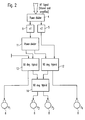
- FIG. 1 shows the general concept of a direct 6-port receiver based on non-coherent detection according to the present invention.
- a received RF-signal is passed through a band pass filter 1, LNA- amplified 2, again passed through another band pass filter 3 and then output to a power divider 4.
- the power divider 4 divides the supplied RF-signal in two branches S1 and S2.
- One branch S1 is output to a first delay line 6 with a delay constant ⁇ 1.
- the other branch's output to a second delay line 5 with a delay constant ⁇ 2 which is different to the delay constant ⁇ 1 of the first delay line 6.
- the two branches S1, S2 divided by the power divider 4 and delayed by the first 6 and second delay line 5 are then input to a passive circuit 7.
- the passive circuit 7 provides for different linear combinations of the two input signals.
- the passive circuit 7 preferably only comprises linear passive components such as detector diodes.
- the amplitude, i.e. the power of the at least three linear combinations calculated by the passive circuit 7 and preferably the four linear combinations provided by the passive circuit 7 are then detected by power reading circuits 8.
- the power reading circuits 8 preferably comprise only detector diodes. As it has already been stated, the minimum number of detected power levels detected by the power reading circuits 8 is three. In the example shown in figure 1 the passive circuit 7 provides for 4 linear combinations of the two input signals S1 and S2, and therefore four power levels are detected on the four linear combinations. The example of figure 1 therefore provides for a certain redundancy of the entire system.
- the output of the power reading circuits 8, i.e. the detected power levels are then respectively given to circuits 9, which comprise low pass filters and A/D converters.
- the circuitry 9 can comprise DC amplifiers. Therefore the circuitry 9 respectively amplifies the detected power level output by the power reading circuits 8 and converts them digitally.
- the digital output signals of the circuitry 9 are then respectively given to a digital signal processing unit 10.
- the digital signal processing unit 10 provides for a digital filtering of the input signals, a calibration of the system, which will be explained afterwards, the calculation of the I/Q parts of the input signals as well as a further processing such as a demodulation.
- the direct 6-port receiver essentially consists of two inputs (RF-band) approaching a passive RE structure.
- Passive RF structure is defined as a passive circuitry, designed to function in frequency bands beginning of tenths of MHz up to tenths of GHz depending on different realization issues.
- the passive structure contains several (at least three, preferably four) power detectors.
- the outputs of the power detectors 8 are DC voltages which are sampled by the A/D converter 9 after a possible amplification (optionally) and filtering.
- ⁇ 2 can be 0 and the corresponding delay line 6 can be suppressed.
- the relative delay ⁇ between the two branches divided by the power divider 4 is equal or greater than the inverse of the sampling rate of the A/D converter 9.
- the invention allows a detection of vector information, i.e. a phase on the amplitude of the RE signal based only on scalar information (power levels detected by the power reading circuits 8). Therefore the invention allows for a detection of a phase information non-coherently.
- the method how the vector information representing the relation (ratio) between the two branches of the input signal which are delayed relatively to each other (delay lines 5, 6) in the digital signal processing unit 10 will be explained later on.
- a advantage of the invention is that the whole RF front end can be realized with a simple chip if there is no local oscillator.
- Conventional, not necessarily very advanced GAAS or (SI) MMIC technology for lower frequency bands could be utilized for much higher frequency bands 6-port structure, as there are no active components and the main challenge is only to realize detector diodes on a waver. Therefore the invention provides for a cost reduction in the RF-front end due to avoiding the intermediate stages and having less complicated RF-front end structure (without local oscillator circuit, AGC and PLL).
- the detected power levels are A/D converted 9 and then digitally processed.
- the detected analog power levels have not to be A/D converted and can be processed in an analog way.
- an complex signal representing a ratio of the two input RF-signals provided by the power divider 4 is calculating using additional calibration coefficients obtained from a calibration procedure.
- the complex signal can then be further optionally decomposed to I/Q data streams to be further used for a conventional demodulation procedure in a base band.
- additional LNA and additional BPF can be placed after the delay lines 5, 6 or integrated within the delay lines 5,6 before approaching the inputs of the passive circuitry structure 7.
- the passive RF circuit 7 is a circuit including only passive linear components, this can include power dividers, hybrids, couplers, transmission lines, matching elements, resistors, capacitors in a different number of each art of component and compositions.
- a whole passage circuitry can be realized with distributed or lump elements.
- the design of the transmission lines, substrates or reused lump elements is arbitrary and is usually set to optimize the passive circuit 7 to defined bands of interest, which are called RF frequency bands in the following explanation.
- the RF frequency band is a band of interest.
- the RF frequency band represents a frequency band in which the proposed receiver structure functions.
- RF frequency band can also be understood as an intermediate frequency band of a more complex receiver circuitry.
- the proposed receiver functions as a direct conversion circuitry from intermediate frequency to the base band.
- the direct 6-port-receiver according to the present invention can process in that case the intermediate frequency signal obtained from another intermediate frequency or higher RF frequency signal by one of the classic down-conversion techniques.
- the RF frequency signal can take frequency values in the range of 50 MHz to 100 GHz.
- the RF frequency signal is filtered and amplified before approaching the passive circuit 7. Before the first band pass filtering 1 additional structures can be utilized to provide frequency channel assignment if necessary.
- the passive circuit 7 provides for at least three and preferably four linear combinations of the two input signals S 1 and S 2 output by the delay lines 6 and 5, respectively.
- the power levels P 1 , P 2 , P 3 and P 4 are detected by the power reading circuits (power detectors) 8.
- a power detector is a device which converts power of the signals coming in the frequency range of the RF frequency band to a DC voltage information. It can be realized in different technologies. The most usual technology for the practical implementation and realization of the digital 6-point receiver is the realization with common detector diode approach. Detector diodes can be integrated on one chip together with the passive circuit 7. Detector diodes is to be understood as detector diodes with an optional circuitry for temperature compensation.
- the digital signal processing unit 10 calculates a complex signal out of the amplified, filtered and A/D-converted power levels P 1 , P 2 , P 3 and P 4 , which complex signal represents the relation (ratio) between the two input signals S 1 and S 2 .
- the digital signal processing unit 10 is a hardware which allows digital signal processing of the bits coming from the A/D converter 9.
- the basic functions of digital signal processing unit 10 are:
- the calculation of the complex signal as well as the calculation of the calibration coefficients is done using alternatively software digital signal processing capabilities or hardware capabilities (ASIC or similar). This depends on the considered data rates to be processed.
- the processing done by the digital signal processing unit 10 can be realized in conjunction with a demodulation procedure using the same hardware parts (e.g. the same digital signal processing).
- the digital signal processing unit 10 calculates the mentioned complex signal representing the ratio between the two input signal S1 and S2.
- the complex signal is a signal which is calculated in the digital signal processing unit 10 using calibration coefficients and combinations of relative power levels, which are detected by the power reading circuits 8 and presented as ratios of voltages.
- the typical structure of the complex signal with the usual number of power reading circuits 8 (4) is presented in the following equation 2: wherein
- the calibration procedure is a procedure which is necessary in order to obtain calibration coefficients xi, y(i).
- the calibration can be done without disconnecting the physical connections of the system.
- the calibration procedure which can be performed in an off-line approach.
- the system parameters do not alter fast, so that off-line calculations can be performed in the period T.
- the period T is much larger than the signal symbol duration.
- the calibration coefficients are obtained by the calibration process and they are used for relative signal detection in conjunction with power reading.
- initial calibration values are utilized for the calculation of a relative signal.
- a demodulation procedure is executed.
- the demodulation procedure can be performed by the hardware structures (e.g. I/Q demodulator chips) or with the DSP software (e.g. the same DSP which is used for calculation of the calibration coefficients and for calculation of the complex signal).
- the complex signal can be directly utilized for the demodulation without its decomposition in the I- or Q-information (data stream). Due to the inherently proposed non-coherent detection it is necessary to apply a differential processing of the data streams before approaching D/A converters and further I/Q ports of the transmitter modulator.
- the kind of modulation use does not alter the principal functionality of the proposed receiver, so that all kinds of combinations of modulation schemes can be utilized if they are processed differentially before approaching D/A converters and I/Q ports of the transceiver. It is furthermore to be noted that the structure of the passive circuit 7 is invariant.
- the passive circuit 7 consists of ideal sub-circuits which need not to be calibrated. Furthermore ideal linear power reading circuits (power detectors) 8 are considered.
- the passive structure can be as shown in figure 2.
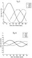
- Figure 5 shows the variation of the relative power levels (voltage at power detectors) as a function of the relative phase difference. In figure 5 it is assumed that there is no amplitude variation between time samples and both incoming signals S1, S2 have the same power level.
- Figure 6 is a representation similar to figure 5, but with the assumption that the incoming signals have a relative power level difference of 20dB.
- the relative power levels are independent of the RF signal level.
- Figure 7 shows a principle calculation required to be performed in the digital signal processing unit 10 of the receiver.
- Figure 7 shows as an example the state that the two signals S1, S2 have the same magnitude in two different time points (QPSK modulation) and the phase difference is 7 ⁇ /8 by detecting and calculating the measured power levels and the calibration coefficients as shown three circles are obtained. Ideally they cross in one point.
- the thus created vector represents the complex ratio of the signals S1, S2 at two different time increments, which time increment is defined by the relative delay provided by the two delay lines 5, 6.
- a mathematical processing is required to calculate the crossing point of the known circles (the circles are defined by the calibration coefficients).
- the vector directing from the origin of the grid to the crossing point of the three circles has a length (amplitude) corresponding to one unit and represents an angle of 157.5° (7 ⁇ /8).
- the fact that the vector has the length corresponding to one unit represents the fact, that the two signals S1, S2 have the same magnitude, as it is the case e.g. for the QPSK modulation.
- Figure 8 shows the case, that the two signals S1, S2 are different in phase and magnitude.
- Figure 8 shows as an example the state that the relative change of the signal is three times in the magnitude and 45.5° ( ⁇ /4) in phase.
- the vector direction from the origin of the grid to the crossing point of the three circles has a length corresponding to 1/3 units and an angle of 45.5° ( ⁇ /4).
- the direct 6-port receiver detects differences between the two signals S1, S2, so that any relative change in signal from one to another time step can be detected. That means that before the transmission of the up-converted signal, the digital data before supplied to the transmitter I/Q modulator via D/A converter have to be differentially processed which is inherently true for DPSK modulation schemes. In case the transmitted digital data are not differentially modulated, reference samples have to be sent in order to provide a reference magnitude and a reference phase for the detection of the absolute values of the modulated digital data.
- the three circles do not cross exactly in the same point. Therefore there is usually some offset in the circles' crossings, which has to be mathematically treated.
- the offset is due to the fact that the calibration coefficients are not optimally obtained.
- a further reason for the offset can be different noise effects.
- Different approaches can be utilized in the signal processing of the digital signal processing unit 10 to "decide" where to place a crossing point. For example the geometric median of the curved triangle can be taken as the crossing point.
- the offset can be neglected in some cases, where a relative low number of the modulation states are considered, as it is the case e.g. for a QPSK modulation scheme.
Landscapes
- Engineering & Computer Science (AREA)
- Computer Networks & Wireless Communication (AREA)
- Signal Processing (AREA)
- Power Engineering (AREA)
- Digital Transmission Methods That Use Modulated Carrier Waves (AREA)
- Superheterodyne Receivers (AREA)
- Mobile Radio Communication Systems (AREA)
Priority Applications (9)
| Application Number | Priority Date | Filing Date | Title |
|---|---|---|---|
| EP97113755A EP0896455B1 (de) | 1997-08-08 | 1997-08-08 | Nichtkohärentes Direktkonversionsempfänger mit Sechs-Tor-Schaltung |
| DE69736892T DE69736892T2 (de) | 1997-08-08 | 1997-08-08 | Nichtkohärentes Direktkonversionsempfänger mit Sechs-Tor-Schaltung |
| CA002241124A CA2241124C (en) | 1997-08-08 | 1998-06-18 | Non-coherent 6-port receiver |
| US09/115,034 US6363125B1 (en) | 1997-08-08 | 1998-07-14 | Non-coherent six-port receiver |
| PCT/EP1998/005032 WO1999008426A1 (en) | 1997-08-08 | 1998-08-07 | Non-coherent six-port receiver |
| CNB988014831A CN1135803C (zh) | 1997-08-08 | 1998-08-07 | 非相干6端口接收机 |
| KR1019997003037A KR100582855B1 (ko) | 1997-08-08 | 1998-08-07 | 넌코히어런트 6-포트 수신기 |
| TW87113127A TW498665B (en) | 1997-08-08 | 1998-08-10 | Non-coherent 6-port receiver |
| JP23803398A JP3982662B2 (ja) | 1997-08-08 | 1998-08-10 | 受信方法及び高周波信号受信機 |
Applications Claiming Priority (1)
| Application Number | Priority Date | Filing Date | Title |
|---|---|---|---|
| EP97113755A EP0896455B1 (de) | 1997-08-08 | 1997-08-08 | Nichtkohärentes Direktkonversionsempfänger mit Sechs-Tor-Schaltung |
Publications (2)
| Publication Number | Publication Date |
|---|---|
| EP0896455A1 true EP0896455A1 (de) | 1999-02-10 |
| EP0896455B1 EP0896455B1 (de) | 2006-11-02 |
Family
ID=8227189
Family Applications (1)
| Application Number | Title | Priority Date | Filing Date |
|---|---|---|---|
| EP97113755A Expired - Lifetime EP0896455B1 (de) | 1997-08-08 | 1997-08-08 | Nichtkohärentes Direktkonversionsempfänger mit Sechs-Tor-Schaltung |
Country Status (8)
| Country | Link |
|---|---|
| US (1) | US6363125B1 (de) |
| EP (1) | EP0896455B1 (de) |
| JP (1) | JP3982662B2 (de) |
| KR (1) | KR100582855B1 (de) |
| CN (1) | CN1135803C (de) |
| CA (1) | CA2241124C (de) |
| DE (1) | DE69736892T2 (de) |
| WO (1) | WO1999008426A1 (de) |
Cited By (3)
| Publication number | Priority date | Publication date | Assignee | Title |
|---|---|---|---|---|
| EP1067675A1 (de) * | 1999-07-08 | 2001-01-10 | Sony International (Europe) GmbH | Kalibrierung eines Empfängers mit N -Toren |
| EP1189338A1 (de) * | 2000-09-06 | 2002-03-20 | Sony International (Europe) GmbH | I/Q Demodulator mit drei Leistungsdetektoren und zwei A/D-Wandlern |
| EP1376852A1 (de) * | 2002-06-20 | 2004-01-02 | Sony International (Europe) GmbH | I/Q Demodulator unter Verwendung eines Sechs-Tor-Schaltung |
Families Citing this family (11)
| Publication number | Priority date | Publication date | Assignee | Title |
|---|---|---|---|---|
| EP1056193B1 (de) * | 1999-05-27 | 2005-04-27 | Sony International (Europe) GmbH | Ein Dreitor-Koppler verwendender Abwärtsumsetzer und Demodulator |
| EP1172927B1 (de) * | 2000-07-11 | 2006-04-12 | Sony Deutschland GmbH | Quadraturdemodulator unter Verwendung von Leistungssensoren |
| KR100531136B1 (ko) * | 2002-09-09 | 2005-11-28 | 주식회사에스지테크놀러지 | 직접 변환 수신기용 6포트 |
| KR100673406B1 (ko) * | 2005-01-26 | 2007-01-24 | 아태위성산업 주식회사 | 지상 휴대전화기에 탑재되는 위성 통신 장치 및 방법 |
| US20090267746A1 (en) * | 2008-04-23 | 2009-10-29 | Martec Corporation | Multi-Port Receiver |
| WO2010007468A1 (en) * | 2008-07-16 | 2010-01-21 | Freescale Semiconductor, Inc. | Method and apparatus for detecting one or more predetermined tones transmitted over a communication network |
| WO2012009757A1 (en) * | 2010-07-21 | 2012-01-26 | Kaelus Pty Ltd | Method and apparatus for locating faults in communications networks |
| US9482735B2 (en) * | 2013-09-11 | 2016-11-01 | King Fahd University Of Petroleum And Minerals | Microwave radio direction finding system |
| CN105187090B (zh) * | 2015-10-14 | 2018-05-15 | 福建奥通迈胜电力科技有限公司 | 一种用于集中器间的高效中继射频通信电路 |
| CN108196235B (zh) * | 2018-02-08 | 2021-04-27 | 北京理工大学 | 一种用于多通道毫米波雷达的幅相校准方法 |
| CN114123980B (zh) * | 2022-01-27 | 2022-05-03 | 电子科技大学 | 基于GaAs单片集成的太赫兹低噪声通信系统收发前端 |
Citations (3)
| Publication number | Priority date | Publication date | Assignee | Title |
|---|---|---|---|---|
| EP0645917A2 (de) * | 1993-09-14 | 1995-03-29 | Nec Corporation | Demodulator |
| EP0692895A2 (de) * | 1994-07-13 | 1996-01-17 | Nec Corporation | Demodulation mit Differenzdetektion |
| EP0805561A2 (de) * | 1996-05-03 | 1997-11-05 | Nokia Mobile Phones Ltd. | Verfahren zur Realisierung eines Direktumsetzempfängers mit einer Sechs-Tor-Schaltung |
Family Cites Families (5)
| Publication number | Priority date | Publication date | Assignee | Title |
|---|---|---|---|---|
| US4104583A (en) * | 1977-08-31 | 1978-08-01 | The United States Of America As Represented By The Secretary Of Commerce | Six-port measuring circuit |
| US4521728A (en) * | 1982-08-23 | 1985-06-04 | Renato Bosisio | Method and a six port network for use in determining complex reflection coefficients of microwave networks |
| FR2707398B1 (fr) * | 1993-07-09 | 1995-08-11 | France Telecom | Dispositif de mesure vectorielle de signaux hyperfréquences de même pulsation, de type jonction à six accès. |
| EP0841756A3 (de) * | 1996-11-07 | 2001-11-28 | Nokia Mobile Phones Ltd. | Verbesserte Korrelatorschaltung für eine Sechs-Tor-Schaltung |
| US6072770A (en) * | 1997-03-04 | 2000-06-06 | At&T Corporation | Method and system providing unified DPSK-PSK signalling for CDMA-based satellite communications |
-
1997
- 1997-08-08 DE DE69736892T patent/DE69736892T2/de not_active Expired - Lifetime
- 1997-08-08 EP EP97113755A patent/EP0896455B1/de not_active Expired - Lifetime
-
1998
- 1998-06-18 CA CA002241124A patent/CA2241124C/en not_active Expired - Fee Related
- 1998-07-14 US US09/115,034 patent/US6363125B1/en not_active Expired - Fee Related
- 1998-08-07 KR KR1019997003037A patent/KR100582855B1/ko not_active Expired - Fee Related
- 1998-08-07 CN CNB988014831A patent/CN1135803C/zh not_active Expired - Fee Related
- 1998-08-07 WO PCT/EP1998/005032 patent/WO1999008426A1/en not_active Ceased
- 1998-08-10 JP JP23803398A patent/JP3982662B2/ja not_active Expired - Fee Related
Patent Citations (3)
| Publication number | Priority date | Publication date | Assignee | Title |
|---|---|---|---|---|
| EP0645917A2 (de) * | 1993-09-14 | 1995-03-29 | Nec Corporation | Demodulator |
| EP0692895A2 (de) * | 1994-07-13 | 1996-01-17 | Nec Corporation | Demodulation mit Differenzdetektion |
| EP0805561A2 (de) * | 1996-05-03 | 1997-11-05 | Nokia Mobile Phones Ltd. | Verfahren zur Realisierung eines Direktumsetzempfängers mit einer Sechs-Tor-Schaltung |
Non-Patent Citations (1)
| Title |
|---|
| LI J ET AL: "A SIX-PORT DIRECT DIGITAL MILLIMETER WAVE RECEIVER", IEEE MTT-S INTERNATIONAL MICROWAVE SYMPOSIUM DIGEST, SAN DIEGO, MAY 23 - 27, 1994, vol. 3, 23 May 1994 (1994-05-23), KUNO H J;WEN C P (EDITORS), pages 1659 - 1662, XP000512814 * |
Cited By (6)
| Publication number | Priority date | Publication date | Assignee | Title |
|---|---|---|---|---|
| EP1067675A1 (de) * | 1999-07-08 | 2001-01-10 | Sony International (Europe) GmbH | Kalibrierung eines Empfängers mit N -Toren |
| JP2001060982A (ja) * | 1999-07-08 | 2001-03-06 | Sony Internatl Europ Gmbh | 較正方法及び較正装置 |
| US6735261B1 (en) | 1999-07-08 | 2004-05-11 | Sony International (Europe) Gmbh | Calibration of a N-port receiver |
| EP1189338A1 (de) * | 2000-09-06 | 2002-03-20 | Sony International (Europe) GmbH | I/Q Demodulator mit drei Leistungsdetektoren und zwei A/D-Wandlern |
| US6999528B2 (en) | 2000-09-06 | 2006-02-14 | Sony International (Europe) Gmbh | I/Q demodulator device with three power detectors and two A/D converters |
| EP1376852A1 (de) * | 2002-06-20 | 2004-01-02 | Sony International (Europe) GmbH | I/Q Demodulator unter Verwendung eines Sechs-Tor-Schaltung |
Also Published As
| Publication number | Publication date |
|---|---|
| CN1135803C (zh) | 2004-01-21 |
| CN1244322A (zh) | 2000-02-09 |
| KR100582855B1 (ko) | 2006-05-24 |
| JP3982662B2 (ja) | 2007-09-26 |
| US6363125B1 (en) | 2002-03-26 |
| CA2241124C (en) | 2008-11-25 |
| WO1999008426A1 (en) | 1999-02-18 |
| KR20000068733A (ko) | 2000-11-25 |
| CA2241124A1 (en) | 1999-02-08 |
| DE69736892T2 (de) | 2007-03-15 |
| EP0896455B1 (de) | 2006-11-02 |
| DE69736892D1 (de) | 2006-12-14 |
| JPH11127209A (ja) | 1999-05-11 |
Similar Documents
| Publication | Publication Date | Title |
|---|---|---|
| US6922555B1 (en) | Phase interpolation receiver for angle modulated RF signals | |
| EP1014562B1 (de) | Demodulator und Verfahren zur Demodulation von modulierten RF Signalen | |
| US6363125B1 (en) | Non-coherent six-port receiver | |
| US20090215423A1 (en) | Multi-port correlator and receiver having the same | |
| EP0937339B1 (de) | Kalibrierung eines n-port-empfängers | |
| EP1172927B1 (de) | Quadraturdemodulator unter Verwendung von Leistungssensoren | |
| EP1089445B1 (de) | Drei-Tor Struktur mit modulierten Injektionssignal | |
| EP1056193B1 (de) | Ein Dreitor-Koppler verwendender Abwärtsumsetzer und Demodulator | |
| EP1189338A1 (de) | I/Q Demodulator mit drei Leistungsdetektoren und zwei A/D-Wandlern | |
| EP0957614A1 (de) | N-Tordemodulator für phasensprung- oder quadraturamplitudenmodulierte Signale | |
| Gagne et al. | Low cost architecture of direct conversion digital receiver | |
| JP2791402B2 (ja) | 周波数安定化回路 |
Legal Events
| Date | Code | Title | Description |
|---|---|---|---|
| PUAI | Public reference made under article 153(3) epc to a published international application that has entered the european phase |
Free format text: ORIGINAL CODE: 0009012 |
|
| AK | Designated contracting states |
Kind code of ref document: A1 Designated state(s): DE FI FR GB IT SE |
|
| AX | Request for extension of the european patent |
Free format text: AL;LT;LV;RO;SI |
|
| 17P | Request for examination filed |
Effective date: 19990618 |
|
| AKX | Designation fees paid |
Free format text: DE FI FR GB IT SE |
|
| RAP1 | Party data changed (applicant data changed or rights of an application transferred) |
Owner name: SONY INTERNATIONAL (EUROPE) GMBH |
|
| 17Q | First examination report despatched |
Effective date: 20040428 |
|
| RAP1 | Party data changed (applicant data changed or rights of an application transferred) |
Owner name: SONY DEUTSCHLAND GMBH |
|
| RAP1 | Party data changed (applicant data changed or rights of an application transferred) |
Owner name: SONY DEUTSCHLAND GMBH |
|
| RAP1 | Party data changed (applicant data changed or rights of an application transferred) |
Owner name: SONY DEUTSCHLAND GMBH |
|
| GRAP | Despatch of communication of intention to grant a patent |
Free format text: ORIGINAL CODE: EPIDOSNIGR1 |
|
| GRAS | Grant fee paid |
Free format text: ORIGINAL CODE: EPIDOSNIGR3 |
|
| GRAA | (expected) grant |
Free format text: ORIGINAL CODE: 0009210 |
|
| AK | Designated contracting states |
Kind code of ref document: B1 Designated state(s): DE FI FR GB IT SE |
|
| PG25 | Lapsed in a contracting state [announced via postgrant information from national office to epo] |
Ref country code: IT Free format text: LAPSE BECAUSE OF FAILURE TO SUBMIT A TRANSLATION OF THE DESCRIPTION OR TO PAY THE FEE WITHIN THE PRESCRIBED TIME-LIMIT;WARNING: LAPSES OF ITALIAN PATENTS WITH EFFECTIVE DATE BEFORE 2007 MAY HAVE OCCURRED AT ANY TIME BEFORE 2007. THE CORRECT EFFECTIVE DATE MAY BE DIFFERENT FROM THE ONE RECORDED. Effective date: 20061102 Ref country code: FI Free format text: LAPSE BECAUSE OF FAILURE TO SUBMIT A TRANSLATION OF THE DESCRIPTION OR TO PAY THE FEE WITHIN THE PRESCRIBED TIME-LIMIT Effective date: 20061102 |
|
| REG | Reference to a national code |
Ref country code: GB Ref legal event code: FG4D |
|
| REF | Corresponds to: |
Ref document number: 69736892 Country of ref document: DE Date of ref document: 20061214 Kind code of ref document: P |
|
| PG25 | Lapsed in a contracting state [announced via postgrant information from national office to epo] |
Ref country code: SE Free format text: LAPSE BECAUSE OF FAILURE TO SUBMIT A TRANSLATION OF THE DESCRIPTION OR TO PAY THE FEE WITHIN THE PRESCRIBED TIME-LIMIT Effective date: 20070202 |
|
| EN | Fr: translation not filed | ||
| PLBE | No opposition filed within time limit |
Free format text: ORIGINAL CODE: 0009261 |
|
| STAA | Information on the status of an ep patent application or granted ep patent |
Free format text: STATUS: NO OPPOSITION FILED WITHIN TIME LIMIT |
|
| 26N | No opposition filed |
Effective date: 20070803 |
|
| PG25 | Lapsed in a contracting state [announced via postgrant information from national office to epo] |
Ref country code: FR Free format text: LAPSE BECAUSE OF FAILURE TO SUBMIT A TRANSLATION OF THE DESCRIPTION OR TO PAY THE FEE WITHIN THE PRESCRIBED TIME-LIMIT Effective date: 20070615 |
|
| PG25 | Lapsed in a contracting state [announced via postgrant information from national office to epo] |
Ref country code: FR Free format text: LAPSE BECAUSE OF FAILURE TO SUBMIT A TRANSLATION OF THE DESCRIPTION OR TO PAY THE FEE WITHIN THE PRESCRIBED TIME-LIMIT Effective date: 20061102 |
|
| PGFP | Annual fee paid to national office [announced via postgrant information from national office to epo] |
Ref country code: DE Payment date: 20100823 Year of fee payment: 14 |
|
| PGFP | Annual fee paid to national office [announced via postgrant information from national office to epo] |
Ref country code: GB Payment date: 20100819 Year of fee payment: 14 |
|
| GBPC | Gb: european patent ceased through non-payment of renewal fee |
Effective date: 20110808 |
|
| REG | Reference to a national code |
Ref country code: DE Ref legal event code: R119 Ref document number: 69736892 Country of ref document: DE Effective date: 20120301 |
|
| PG25 | Lapsed in a contracting state [announced via postgrant information from national office to epo] |
Ref country code: GB Free format text: LAPSE BECAUSE OF NON-PAYMENT OF DUE FEES Effective date: 20110808 |
|
| PG25 | Lapsed in a contracting state [announced via postgrant information from national office to epo] |
Ref country code: DE Free format text: LAPSE BECAUSE OF NON-PAYMENT OF DUE FEES Effective date: 20120301 |