EP0898302A1 - Reaktor und Verfahren zum Behandlung eines Halbleitersubstrats - Google Patents
Reaktor und Verfahren zum Behandlung eines Halbleitersubstrats Download PDFInfo
- Publication number
- EP0898302A1 EP0898302A1 EP98650052A EP98650052A EP0898302A1 EP 0898302 A1 EP0898302 A1 EP 0898302A1 EP 98650052 A EP98650052 A EP 98650052A EP 98650052 A EP98650052 A EP 98650052A EP 0898302 A1 EP0898302 A1 EP 0898302A1
- Authority
- EP
- European Patent Office
- Prior art keywords
- substrate
- gas
- housing
- reactor according
- photon density
- Prior art date
- Legal status (The legal status is an assumption and is not a legal conclusion. Google has not performed a legal analysis and makes no representation as to the accuracy of the status listed.)
- Granted
Links
Images

Classifications
-
- C—CHEMISTRY; METALLURGY
- C23—COATING METALLIC MATERIAL; COATING MATERIAL WITH METALLIC MATERIAL; CHEMICAL SURFACE TREATMENT; DIFFUSION TREATMENT OF METALLIC MATERIAL; COATING BY VACUUM EVAPORATION, BY SPUTTERING, BY ION IMPLANTATION OR BY CHEMICAL VAPOUR DEPOSITION, IN GENERAL; INHIBITING CORROSION OF METALLIC MATERIAL OR INCRUSTATION IN GENERAL
- C23C—COATING METALLIC MATERIAL; COATING MATERIAL WITH METALLIC MATERIAL; SURFACE TREATMENT OF METALLIC MATERIAL BY DIFFUSION INTO THE SURFACE, BY CHEMICAL CONVERSION OR SUBSTITUTION; COATING BY VACUUM EVAPORATION, BY SPUTTERING, BY ION IMPLANTATION OR BY CHEMICAL VAPOUR DEPOSITION, IN GENERAL
- C23C16/00—Chemical coating by decomposition of gaseous compounds, without leaving reaction products of surface material in the coating, i.e. chemical vapour deposition [CVD] processes
- C23C16/44—Chemical coating by decomposition of gaseous compounds, without leaving reaction products of surface material in the coating, i.e. chemical vapour deposition [CVD] processes characterised by the method of coating
- C23C16/455—Chemical coating by decomposition of gaseous compounds, without leaving reaction products of surface material in the coating, i.e. chemical vapour deposition [CVD] processes characterised by the method of coating characterised by the method used for introducing gases into reaction chamber or for modifying gas flows in reaction chamber
- C23C16/45561—Gas plumbing upstream of the reaction chamber
-
- C—CHEMISTRY; METALLURGY
- C23—COATING METALLIC MATERIAL; COATING MATERIAL WITH METALLIC MATERIAL; CHEMICAL SURFACE TREATMENT; DIFFUSION TREATMENT OF METALLIC MATERIAL; COATING BY VACUUM EVAPORATION, BY SPUTTERING, BY ION IMPLANTATION OR BY CHEMICAL VAPOUR DEPOSITION, IN GENERAL; INHIBITING CORROSION OF METALLIC MATERIAL OR INCRUSTATION IN GENERAL
- C23C—COATING METALLIC MATERIAL; COATING MATERIAL WITH METALLIC MATERIAL; SURFACE TREATMENT OF METALLIC MATERIAL BY DIFFUSION INTO THE SURFACE, BY CHEMICAL CONVERSION OR SUBSTITUTION; COATING BY VACUUM EVAPORATION, BY SPUTTERING, BY ION IMPLANTATION OR BY CHEMICAL VAPOUR DEPOSITION, IN GENERAL
- C23C16/00—Chemical coating by decomposition of gaseous compounds, without leaving reaction products of surface material in the coating, i.e. chemical vapour deposition [CVD] processes
- C23C16/44—Chemical coating by decomposition of gaseous compounds, without leaving reaction products of surface material in the coating, i.e. chemical vapour deposition [CVD] processes characterised by the method of coating
- C23C16/455—Chemical coating by decomposition of gaseous compounds, without leaving reaction products of surface material in the coating, i.e. chemical vapour deposition [CVD] processes characterised by the method of coating characterised by the method used for introducing gases into reaction chamber or for modifying gas flows in reaction chamber
- C23C16/45563—Gas nozzles
- C23C16/45565—Shower nozzles
-
- C—CHEMISTRY; METALLURGY
- C23—COATING METALLIC MATERIAL; COATING MATERIAL WITH METALLIC MATERIAL; CHEMICAL SURFACE TREATMENT; DIFFUSION TREATMENT OF METALLIC MATERIAL; COATING BY VACUUM EVAPORATION, BY SPUTTERING, BY ION IMPLANTATION OR BY CHEMICAL VAPOUR DEPOSITION, IN GENERAL; INHIBITING CORROSION OF METALLIC MATERIAL OR INCRUSTATION IN GENERAL
- C23C—COATING METALLIC MATERIAL; COATING MATERIAL WITH METALLIC MATERIAL; SURFACE TREATMENT OF METALLIC MATERIAL BY DIFFUSION INTO THE SURFACE, BY CHEMICAL CONVERSION OR SUBSTITUTION; COATING BY VACUUM EVAPORATION, BY SPUTTERING, BY ION IMPLANTATION OR BY CHEMICAL VAPOUR DEPOSITION, IN GENERAL
- C23C16/00—Chemical coating by decomposition of gaseous compounds, without leaving reaction products of surface material in the coating, i.e. chemical vapour deposition [CVD] processes
- C23C16/44—Chemical coating by decomposition of gaseous compounds, without leaving reaction products of surface material in the coating, i.e. chemical vapour deposition [CVD] processes characterised by the method of coating
- C23C16/455—Chemical coating by decomposition of gaseous compounds, without leaving reaction products of surface material in the coating, i.e. chemical vapour deposition [CVD] processes characterised by the method of coating characterised by the method used for introducing gases into reaction chamber or for modifying gas flows in reaction chamber
-
- C—CHEMISTRY; METALLURGY
- C23—COATING METALLIC MATERIAL; COATING MATERIAL WITH METALLIC MATERIAL; CHEMICAL SURFACE TREATMENT; DIFFUSION TREATMENT OF METALLIC MATERIAL; COATING BY VACUUM EVAPORATION, BY SPUTTERING, BY ION IMPLANTATION OR BY CHEMICAL VAPOUR DEPOSITION, IN GENERAL; INHIBITING CORROSION OF METALLIC MATERIAL OR INCRUSTATION IN GENERAL
- C23C—COATING METALLIC MATERIAL; COATING MATERIAL WITH METALLIC MATERIAL; SURFACE TREATMENT OF METALLIC MATERIAL BY DIFFUSION INTO THE SURFACE, BY CHEMICAL CONVERSION OR SUBSTITUTION; COATING BY VACUUM EVAPORATION, BY SPUTTERING, BY ION IMPLANTATION OR BY CHEMICAL VAPOUR DEPOSITION, IN GENERAL
- C23C16/00—Chemical coating by decomposition of gaseous compounds, without leaving reaction products of surface material in the coating, i.e. chemical vapour deposition [CVD] processes
- C23C16/44—Chemical coating by decomposition of gaseous compounds, without leaving reaction products of surface material in the coating, i.e. chemical vapour deposition [CVD] processes characterised by the method of coating
- C23C16/455—Chemical coating by decomposition of gaseous compounds, without leaving reaction products of surface material in the coating, i.e. chemical vapour deposition [CVD] processes characterised by the method of coating characterised by the method used for introducing gases into reaction chamber or for modifying gas flows in reaction chamber
- C23C16/45519—Inert gas curtains
-
- C—CHEMISTRY; METALLURGY
- C23—COATING METALLIC MATERIAL; COATING MATERIAL WITH METALLIC MATERIAL; CHEMICAL SURFACE TREATMENT; DIFFUSION TREATMENT OF METALLIC MATERIAL; COATING BY VACUUM EVAPORATION, BY SPUTTERING, BY ION IMPLANTATION OR BY CHEMICAL VAPOUR DEPOSITION, IN GENERAL; INHIBITING CORROSION OF METALLIC MATERIAL OR INCRUSTATION IN GENERAL
- C23C—COATING METALLIC MATERIAL; COATING MATERIAL WITH METALLIC MATERIAL; SURFACE TREATMENT OF METALLIC MATERIAL BY DIFFUSION INTO THE SURFACE, BY CHEMICAL CONVERSION OR SUBSTITUTION; COATING BY VACUUM EVAPORATION, BY SPUTTERING, BY ION IMPLANTATION OR BY CHEMICAL VAPOUR DEPOSITION, IN GENERAL
- C23C16/00—Chemical coating by decomposition of gaseous compounds, without leaving reaction products of surface material in the coating, i.e. chemical vapour deposition [CVD] processes
- C23C16/44—Chemical coating by decomposition of gaseous compounds, without leaving reaction products of surface material in the coating, i.e. chemical vapour deposition [CVD] processes characterised by the method of coating
- C23C16/458—Chemical coating by decomposition of gaseous compounds, without leaving reaction products of surface material in the coating, i.e. chemical vapour deposition [CVD] processes characterised by the method of coating characterised by the method used for supporting substrates in the reaction chamber
- C23C16/4582—Rigid and flat substrates, e.g. plates or discs
- C23C16/4583—Rigid and flat substrates, e.g. plates or discs the substrate being supported substantially horizontally
- C23C16/4586—Elements in the interior of the support, e.g. electrodes, heating or cooling devices
-
- C—CHEMISTRY; METALLURGY
- C23—COATING METALLIC MATERIAL; COATING MATERIAL WITH METALLIC MATERIAL; CHEMICAL SURFACE TREATMENT; DIFFUSION TREATMENT OF METALLIC MATERIAL; COATING BY VACUUM EVAPORATION, BY SPUTTERING, BY ION IMPLANTATION OR BY CHEMICAL VAPOUR DEPOSITION, IN GENERAL; INHIBITING CORROSION OF METALLIC MATERIAL OR INCRUSTATION IN GENERAL
- C23C—COATING METALLIC MATERIAL; COATING MATERIAL WITH METALLIC MATERIAL; SURFACE TREATMENT OF METALLIC MATERIAL BY DIFFUSION INTO THE SURFACE, BY CHEMICAL CONVERSION OR SUBSTITUTION; COATING BY VACUUM EVAPORATION, BY SPUTTERING, BY ION IMPLANTATION OR BY CHEMICAL VAPOUR DEPOSITION, IN GENERAL
- C23C16/00—Chemical coating by decomposition of gaseous compounds, without leaving reaction products of surface material in the coating, i.e. chemical vapour deposition [CVD] processes
- C23C16/44—Chemical coating by decomposition of gaseous compounds, without leaving reaction products of surface material in the coating, i.e. chemical vapour deposition [CVD] processes characterised by the method of coating
- C23C16/48—Chemical coating by decomposition of gaseous compounds, without leaving reaction products of surface material in the coating, i.e. chemical vapour deposition [CVD] processes characterised by the method of coating by irradiation, e.g. photolysis, radiolysis, particle radiation
- C23C16/481—Chemical coating by decomposition of gaseous compounds, without leaving reaction products of surface material in the coating, i.e. chemical vapour deposition [CVD] processes characterised by the method of coating by irradiation, e.g. photolysis, radiolysis, particle radiation by radiant heating of the substrate
-
- C—CHEMISTRY; METALLURGY
- C23—COATING METALLIC MATERIAL; COATING MATERIAL WITH METALLIC MATERIAL; CHEMICAL SURFACE TREATMENT; DIFFUSION TREATMENT OF METALLIC MATERIAL; COATING BY VACUUM EVAPORATION, BY SPUTTERING, BY ION IMPLANTATION OR BY CHEMICAL VAPOUR DEPOSITION, IN GENERAL; INHIBITING CORROSION OF METALLIC MATERIAL OR INCRUSTATION IN GENERAL
- C23C—COATING METALLIC MATERIAL; COATING MATERIAL WITH METALLIC MATERIAL; SURFACE TREATMENT OF METALLIC MATERIAL BY DIFFUSION INTO THE SURFACE, BY CHEMICAL CONVERSION OR SUBSTITUTION; COATING BY VACUUM EVAPORATION, BY SPUTTERING, BY ION IMPLANTATION OR BY CHEMICAL VAPOUR DEPOSITION, IN GENERAL
- C23C16/00—Chemical coating by decomposition of gaseous compounds, without leaving reaction products of surface material in the coating, i.e. chemical vapour deposition [CVD] processes
- C23C16/44—Chemical coating by decomposition of gaseous compounds, without leaving reaction products of surface material in the coating, i.e. chemical vapour deposition [CVD] processes characterised by the method of coating
- C23C16/52—Controlling or regulating the coating process
-
- H—ELECTRICITY
- H10—SEMICONDUCTOR DEVICES; ELECTRIC SOLID-STATE DEVICES NOT OTHERWISE PROVIDED FOR
- H10P—GENERIC PROCESSES OR APPARATUS FOR THE MANUFACTURE OR TREATMENT OF DEVICES COVERED BY CLASS H10
- H10P72/00—Handling or holding of wafers, substrates or devices during manufacture or treatment thereof
- H10P72/04—Apparatus for manufacture or treatment
- H10P72/0431—Apparatus for thermal treatment
- H10P72/0436—Apparatus for thermal treatment mainly by radiation
Definitions
- the present invention relates to a processing reactor and, more particularly, to a processing reactor for the thermal processing and chemical deposition of thin film applications on a substrate, such as semiconductor wafer, in which the temperature of the substrate can be accurately monitored and the injection of gas into the chamber can be controlled to provide better control of the substrate processing.
- semiconductor substrates are heated during various temperature activated processes for example, during film deposition, oxide growth, etching, and thermal annealing.
- the control of deposition and annealing processes depends on the control of the gas flow and pressure and the wafer temperature.
- the adhesion of the deposition to the substrate may vary as well.
- the temperature in one region of the substrate is higher or lower than the temperature in another region of the substrate, a temperature gradient within the substrate material is formed. This temperature gradient produces thermal moments in the substrates which in turn induce radial local thermal stresses in the substrate. These local thermal stresses can reduce the substrate's strength and, furthermore, damage the substrate. Therefore, knowing the temperature of the wafer is important in determining the thermal diffusion depths of surface implanted dopants, the deposited film thickness, and the material constitution quality and annealed or reflowed characteristics.
- Direct methods which include the use of contact probes, such as thermocouples or resistance wire thermometers, are generally not suitable for substrate processing because direct contact between the probes and the substrate contaminates the device structure.
- indirect measuring methods are used, such as the use of preheated platforms that are calibrated prior to processing.
- this method is not typically accurate.
- the temperature of the back side of the substrate is calibrated or monitored, but such methods also lead to significant errors due to the large variances between the back side and device side surface characteristics that lead to different substrate temperatures.
- the patterns of the specific devices being processed, the type of material being deposited or annealed, the degree of the roughness of the surface, and the operating temperature all affect the characteristics of the substrate surface and define what is known as the surface emissivity of the substrate.
- a non-contact temperature measuring device in U.S. Patent No. 5,310,260 to Schietinger et al.
- the device includes two sapphire optical fibre probes, with one of the probes directed to the lamp source providing the heat to the wafer and the other probe directed to the wafer itself.
- Each fiber probe sends its respective signal to a measuringinstrument which converts the photon density measured by the probe to an electrical current.
- the ratio of the two signals provides a measure of the surface reflectivity, which approximates the total hemispherical reflectivity.
- this method can only be used with an AC source lamp and when the lamp shines directly on the wafer.
- optical fiber sensors Since two optical fiber probes must be used in order to implement this technique, the characteristics of each probe must be accurately detailed in order to obtain accurate emissivity measurements. In the event that one of the probes must be replaced, a total system re-calibration is required. Furthermore, this method cannot be used in chambers in which thin films are deposited, etched, or sputtered since the thin films will also deposit on the optical fiber photon density sensors and drastically alter the results and render the measurement method inoperative. Moreover, the optical fiber sensors are always directed at one fixed area of the wafer. Since different parts of the wafer may have different device patterns and, therefore, may have different local emissivities, the temperature measurement and control would be limited in value as it would represent the emissivity information only for that specific area rather than the average surface topology of the substrate.
- the uniformity of film deposition is affected by uniformity of the delivery of the process gas.
- Good process uniformity usually requires adjustments and optimizations for both the wafer temperature uniformity and the gas flow pattern of the process gas.
- the reactant gas is delivered through a single port, which injects gas into the chamber above the wafer. Due to the geometry of the wafer, the resulting deposition of the gas onto the wafer is not uniform.
- shower-like gas injection systems have been developed in which separate gases are injected in a shower-like pattern over the entire substrate area.
- gas delivery systems fill the entire chamber volume and, thus, deposit films on the substrate as well as the chamber walls. Consequently, these gas delivery systems preclude the use of any optical instruments for non-contact temperature measurement and in-situ film methodology.
- a processing reactor which can deliver heat to a substrate in a uniform manner and can accurately monitor the temperature of the substrate during processing and adjust the profile of the applied heat as needed to achieve optimal processing of the substrate. Furthermore, there is a need for a processing reactor which can deliver and direct the flow of gas to the substrate during processing so that the substrate receives a uniform deposition of thin film of the process gas or gases in a discrete area on the substrate.
- One form of the invention provides a reactor having a processing chamber with an emissivity measuring device and improved gas injection system.
- the emissivity measuring device measures the photon density from a light source, which is housed in the processing chamber, and the reflected photon density off a substrate, which is processed in the processing chamber. These measurements are then used to determine the emissivity and, ultimately, the temperature of the substrate with a high degree of accuracy.
- the emissivity measuring device includes a communications cable which includes a photon or emissivity sensor that is positioned in the processing chamber.
- the photon density sensor is adapted to move between a first position wherein the photon density sensor is directed to the light source for measuring the incident photon density of the light and a second position wherein the photon density sensor is directed toward the substrate for measuring the reflected photon density off the substrate.
- the gas injection system is adapted to inject and direct at least one gas onto a discrete area of the substrate.
- the reactor is, therefore, particularly suitable for use in a semiconductor fabrication environment where the control of heating and injection of gas must be maintained in order to produce uniform process variables during the fabrication of semiconductor devices.
- the emissivity measuring device comprises first and second communication cables.
- the first communication cable includes the photon density sensor and is in communication with the second cable for sending signals from the photon density sensor to a processor.
- the first and second communication cables comprise optical communication cables.
- the first communication cable may comprise a sapphire optical communication cable
- the second communication cable may comprise a quartz optical communication cable.
- the first and second communications cables are interconnected by a slip connection so that the first communication cable can be rotated between the first and second positions by a driver, for example a motor.
- a reactor for processing a substrate in another form of the invention, includes a first housing, which defines a processing chamber and supports a light source.
- a second housing is rotatably supported in the first housing and is adapted to rotatably support the substrate in the processing chamber.
- a heater for heating the substrate is supported by the first housing and is enclosed in the second housing.
- a photon density sensor extends into the first housing for measuring the emissivity of the substrate, which is adapted to move between a first position wherein the photon density sensor is directed to the light source and a second position wherein the photon density sensor is positioned for directing toward the substrate.
- the reactor further includes a plurality of gas injectors, the gas injectors being grouped into at least two groups of gas injectors, with each group of gas injectors being adapted to inject at least one gas into the processing chamber of the reactor onto a discrete area of the substrate.
- each group of injectors is adapted to selectively deliver at least one reactant gas and an inert gas.
- each group of gas injectors is adapted to be independently controlled whereby flow of gas through each group of gas injectors can be independently adjusted.
- the gas injectors in each group of gas injectors may be arranged in a uniform pattern for directing a uniform flow of a gas toward the substrate.
- the reactor also preferably includes an exhaust manifold for removing unreacted gas from the processing chamber.
- the gas injectors are arranged in pattern having a greater concentration of gas injectors in a peripheral region and a smaller concentration of gas injectors in a central region of the substrate whereby the gas injected by the gas injectors produces a uniform deposition on the substrate.
- a method of processing a semiconductor substrate includes supporting the substrate in a sealed processing chamber.
- the substrate is rotated and heated in the processing chamber in which at least one reactant gas is injected.
- a photon density sensor for measuring the emissivity of the substrate is positioned in the processing chamber and is first directed to a light, which is provided in the chamber, for measuring the incident photon density from the light and then repositioned to direct the photon density sensor to the substrate to measure the reflected photon density off the substrate.
- the incident photon density is compared to the reflected photon density to calculate the substrate temperature.
- the reactor of the present invention provides numerous advantages over prior known reactors.
- the reactor provides a single substrate photon density sensor which can be used to accurately determine the temperature of the substrate during processing.
- the single photon density sensor eliminates the need for recalibration and complex calculations detailing the characteristics of each sensor associated with temperature measuring devices having two sensors.
- the reactor provides a gas injection system which directs one or more reactant gases to the substrate during processing in a controlled manner and directs the gas or gases to discrete regions of the substrate so that emissivity measurements and temperature calculations can be performed in the processing chamber during the injection of the gas or gases without impairment from undesirable film depositions on the emissivity measurement devices.
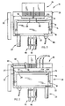
- reactor 10 comprises a single wafer processing reactor that is suitable for performing various fabrication processes on a semiconductor substrate 12, such as a semiconductor wafer.
- Reactor 10 is particularly suitable for thermal processing of a semiconductor wafer.
- thermal processes include thermal annealing of a semiconductor wafer and thermal reflow of boro-phosphorous gasses, and chemical vapor deposition of thin film applications, such as high temperature oxide, low temperature oxide, high temperature nitride, doped and undoped polysilicon, silicon epitaxial and tungsten metal and tungsten silicide films, in the fabrication of a semiconductor device.
- reactor 10 includes a heater assembly 14, which delivers heat to the substrate 12 in a uniform manner, a gas injection assembly 34, which selectively delivers and directs gas to a discrete region of the substrate in a uniform and controlled manner, and an emissivity measurement assembly 60, which permits continuous emissivity measurement of the average surface area of the device side of the substrate during processing so that the amount and/or the profile of the heat being delivered to the substrate during processing may be adjusted.
- reactor 10 includes a heater assembly 14, which is enclosed in a heater housing 16.
- Heater assembly 14 is designed to deliver radiant heat to substrate 12 in a manner such that the temperature in the substrate is substantially uniform.
- heater assembly 14 includes an array of heating elements such as linear tungsten-halogen lamps (not shown), which emit peak radiation at 0.95 microns and are layered to form a plurality of heating zones, which provide a concentrated heating profile with a greater amount of heat being applied to the outer perimeter of the substrate than the center of the substrate.
- heating elements such as linear tungsten-halogen lamps (not shown), which emit peak radiation at 0.95 microns and are layered to form a plurality of heating zones, which provide a concentrated heating profile with a greater amount of heat being applied to the outer perimeter of the substrate than the center of the substrate.
- Heater assembly 14 is enclosed in heater housing 16, which is mounted on a rotatable base 18.
- Heater housing 16 is made from a suitable material, such as a ceramic, graphite, or, more preferably, silicon graphite coated graphite, or the like.
- Heater assembly 14, heater housing 16, and rotatable base 18 are enclosed and vacuum sealed in an outer, reactor housing 20 and are supported on a base wall 22 of reactor housing 20.
- Reactor housing 20 may be formed from a variety of metal materials. For example, aluminium is suitable in some applications, whereas stainless steel is more suitable in others. The choice of material is driven by the type of chemicals used during the deposition process and their reactivity with respect to the metal of choice, as is understood by those persons skilled in the art.
- the chamber walls are typically water cooled to approximately 45-75 degrees Fahrenheit by a conventional recirculating chilled water flow system, which is commonly known in the art.
- base 18 and housing 16 are rotatably supported on base wall 22 of housing and are preferably rotated using a conventional magnetically coupled drive mechanism 23, or other suitable driving device which can impart rotation to base 18 through a vacuum seal.
- the revolutions per minute (rpm) of base 18 and housing 16 may be preset, for example preferably in a range of 5 to 60 rpm depending on the specific process, again as is understood by those persons skilled in the art.
- reactor housing 20 includes a cylindrical outer wall 24 and a cover 26 which extends over cylindrical outer wall 24.
- Substrate 12 is supported in reactor housing 20 on a platform 28, which is made from a suitable material, such as silicon carbide coated graphite, quartz, pure silicon carbide, alumina, zirconia, aluminium, steel, or the like, and is oriented with its device side 12a directed toward cover 26.
- a suitable material such as silicon carbide coated graphite, quartz, pure silicon carbide, alumina, zirconia, aluminium, steel, or the like.
- Platform 28 is seated and supported in a recess or central opening 16a provided in a top wall 27 of housing 16 and spaced from cover 26 and substantially extends over and completely cover opening 16a. Consequently, heater assembly 14 is completely enclosed by heater housing 16 and platform 28, which when placed on top of the housing 16, completes the enclosure of heater assembly 14.
- Platform 28 can accommodate various substrate sizes and, in particular, can accommodate substrates with 150, 200 and 300 mm diameters.
- the space between platform 28 and the lower surface 26a of cover 26 defines an evacuated process chamber 30, which is evacuated through the vacuum exhaust parts placed in a gas injector assembly 34.
- substrate 12 is introduced into evacuated chamber 30 through a chamber valve 32 and is placed on platform 28 by a conventional wafer transport device (not shown), such as an automated transport robot.
- reactor 10 further includes gas injection manifold 34 which injects one or more gases onto a localized or discrete region of the substrate surface wherein thin film deposition takes place.
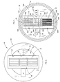
- Gas injection manifold 34 is positioned in cover 26 and includes a plurality of reactive gas injection segments 36, 38, and 40, an inert gas injection ring 41, and an exhaust manifold 44.
- Injection ring 41 injects an inert gas, preferably nitrogen or the like, into processing chamber 30 and directs the inert gas to the perimeter of the substrate to form a gas barrier so that the reactive gases injected through gas injection segments 36, 38, and 40 are confined to the area of the substrate directly below the respective segments 36, 38, and 40 due to the placement of vacuum exhaust manifold 44 adjacent gas injection segments 36, 38, and 40.
- gas injection segments 36, 38, and 40 are aligned in a central region of cover 26 to inject one or more gases, reactive and inert gases, into chamber 30.
- Exhaust manifold 44 extends along and adjacent gas injection segments 36, 38, and 40 so that gases directed onto substrate 12 are confined to a discrete area across the substrate, which preferably extends from one side or edge of the substrate to an opposed side or edge of substrate 12. It should be understood that gases injected by gas injection segments 36, 38, and 40 are directed in the general direction substrate 12 and any stray gas molecules which migrate near the region under exhaust manifold 44 will be exhausted from processing chamber 30. Therefore, the gases introduced by gas injection segments 36, 38, and 40 are confined to a discrete volume of processing chamber 30 and to a discrete area of substrate 12.
- Each gas injection segment 36, 38, 40 includes a plurality of channels 36a, 36b, 36c, 36d, 38a, 38b, 38c, 38d 40a, 40b, 40c, and 40d, respectively, which are arranged in a parallel adjacent relationship.
- Each channel 36a, 36b, 36c, 36d, 38a, 38b, 38c, 38d 40a, 40b, 40c, and 40d includes a plurality of injectors or orifices 42.
- Orifices 42 may be arranged in a uniform manner to provide the same flow rate of gas across width of substrate 12.
- one or more channels may include orifices 42 that are arranged in a non-uniform pattern to vary the profile of the gas flow across the substrate.
- the profile of the flow of the gas is adjusted to direct less gas to the center of the substrate than to the regions toward the perimeter of the substrate.
- channels 38a-38d which are generally aligned with the central portion of the substrate, may include one density or concentration of spaced orifices
- channels 36a-36d and 40a-40d which are generally aligned along the peripheral portions of the substrate, may include a higher density or concentration of orifices 42 than channels 38a-38d.
- the flow of gas from the various groups of orifices 42 has a flow profile that varies across the substrate so that the regions over the central region and the peripheral region of the substrate are treated with the same density of gas to achieve a more uniform film deposition on the substrate.
- the number of orifices and the spacing between orifices 42 may be individually adjusted to provide a more uniform flow or to direct more gas to one area of the substrate than another where different devices are being fabricated.
- each orifice 42/ channel 36a, 36b, 36c, 36d, 38a, 38b, 38c, 38d 40a, 40b, 40c, and 40d and/or segments 36, 38, and 40 may be coupled to a valve or regulator (not shown) which may be adjusted using conventional controls to vary the flow of gas from each orifice, channel, or gas injection segment or zone 36, 38, and 40 to adapt the gas flow profile.
- the controls may adjust the sequence of gas flowing from the orifices, channels, or segments.
- each regulator may be adapted for connection with one or more sources of reactant gases.
- each orifice/ channel/ segment/ may be individually controlled so that they can all turn on together, sequence one segment after another, or sequence the segments randomly with various time intervals between each on/off cycle.
- an inert gas may be injected into that segment to control the reaction conditions at the surface of the wafer and to prevent any back flow contamination of reactants.
- the design of a particular duty cycle for each of the segments would, therefore, depend on the thin film process that is being optimized and it would vary from one film to another.
- each of the respective orifices, channels, or gas injection segments 36, 38, 40 may be associated with an injection of a specific gas.
- gas injection zones 36 and 40 may be used to inject gas A while gas injection zone 38 may be used to inject gas B.
- two reactive gases A and B
- a and B may be injected that mix and react on the device side of the substrate.
- gasses can be employed and selectively introduced through the orifices 42, for example, hydrogen, argon, tungsten hexaflouride, or the like, to process substrate 12.
- gas injection manifold 34 includes exhaust manifold 44.
- exhaust manifold 44 extends around segments 36, 38, and 40 to provide an additional boundary beyond which the reactive gases can not extend.
- exhaust manifold also assists in the prevention of back flow contamination of the reactant gases.
- exhaust manifold 44 controls the film deposition on substrate 12 in a manner which results in localized area of film deposition and, therefore, permits the use of an emissivity measurement system, described below.
- Reactor 10 further includes a non-contact emissivity measurement system 60 for measuring the emissivity and calculating the temperature of substrate 12 during the various fabrication processes.
- Emissivity measurement system 60 includes a central processing unit 61 and a pair of fiber optic communication cables 62 and 64 which are coupled together and coupled to central processing unit 61.
- Fiber optic cable 62 preferably comprises a sapphire fiber optic communication cable and extends into cover 26 of reactor housing 20 through a rigid member 66, which provides a vacuum feedthrough to reactor 10. Cable 62 extends through member 66 into a cavity 67 provided in cover 26, which is positioned above platform 28 and substrate 12.
- Member 66 is preferably a cylindrical drive shaft and, more preferably, a stainless steel cylindrical drive shaft, and is rotatably mounted in cover 26.
- Fiber optic cable 62 One end 68 of fiber optic cable 62 is bent or oriented for directing at substrate 12 and light source 72, as will be more fully explained below, with the photon sensing end of cable 62 forming a fiber optic photon density sensor or probe 70.
- the second end portion of cable 62 extends through shaft 66 and into a fiber optic housing 76, which is mounted to an exterior surface of cylindrical wall 24 of housing 20.
- Distal end 62a of cable 62 is slip attached to a distal end 64a of cable 64, which preferably comprises a quartz fiber optic communication cable, in fiber optic housing 76.
- the other end of fiber optic communication cable 64 is then connected to processor 61.
- Processor 61 preferably comprises a measuring instrument, for example a Luxtron Model 100, which converts the photon density measured by fiber optic sensor 70 into an electrical current, which is displayed by processor 61.
- the position of fiber optic sensor 70 is changed by a driver 80, preferably a motor, which is housed in fiber optic housing 76 and which is drivingly coupled to shaft 66.
- Motor 80 includes a drive shaft 81 and a drive wheel 82, which engages and rotates shaft 66 about its longitudinal axis 66a.
- Motor 80 rotates shaft 66, which imparts rotation to fiber optic cable 62, so that the orientation of fiber optic sensor 70 is moved between a first position wherein the fiber optic sensor 70 is directed generally upward toward light source 72 and a second position in which it is directed generally downward to substrate 12. Therefore, end 68 of communication cable 62 is preferably oriented at a right angle with respect to the horizontal axis 62a of communication cable 62.
- sensor 70 can detect the photon density emitted from light source 72 and of the reflected light off substrate.
- Light source 72 preferably comprises a white light source, which emits light at a wavelength so that the wafer optical transmission is minimized, preferably, for example at a 0.95 micron wavelength.
- Emissivity measurement system 60 determines the temperature of substrate 12 by comparing of the radiation emitted by source 72 with that of the radiation emitted by substrate 12.
- Source 72 preferably includes at least one lamp which is a similar construction to the lamps used in heater assembly 14, which are described in pending U.S. patent application entitled RAPID THERMAL PROCESSING HEATER TECHNOLOGY AND METHOD OF USE.
- photon density sensor 70 is spaced and, preferably, located radially outward from gas injection system 34 and exhaust manifold 44 so that the gas, which is injected into chamber 30 and onto substrate 12, does not interfere with the temperature reading of emissivity sensor 70. Since heater assembly 14 is completely enclosed by the heater housing 16, there is no leakage of light from heater assembly 14 into deposition chamber 30, which could impact the readings taken by emissivity sensor 70. This eliminates probe characteristics matching or corrections associated with the conventional temperature measuring devices with two probes. After substrate 12 is placed on platform 28, housing 16 and platform 28 are rotated during processing by drive mechanism 23. When the emissivity of substrate 12 is to be measured, sensor 70 is rotated to view light source 72 directly above substrate 12 and light source 72 is turned on.
- Sensor 70 measures the incident photon density from light source 72. While light source 72 is still on, sensor 70 is rotated from its first position to its second position to view substrate 12 directly below light source 72 while it is rotating. In this position, sensor 70 measures the reflected photon density off the device side 12a of substrate 12. Light source 72 is then turned off. While still viewing substrate 12 directly, sensor 70 measures the emission of photons from heated substrate 12. This last value is subtracted from the reflected radiation value. According to Plank's law, the energy emitted off a given surface is related to the temperature of the surface to the fourth power. The proportionality constant consists of the product of the Stephen-Boltzmann constant and the surface emissivity.
- the surface emissivity is preferably used when determining the temperature of the surface in non-contact methods.
- the following equations are used to calculate the total hemispherical reflectivity of device side 12a of substrate 12 and, subsequently, the emissivity, as given by Kirchoff's law:
- the substrate temperature is then obtained from Plank's equations. This technique is also used when the substrate is hot and, under such application, the base thermal emission from the substrate is subtracted prior to executing the above calculation.
- sensor 70 is left in the second position or wafer viewing position and, thus, constantly yields emissivity data every time source lamp 72 is turned on.
- sensor 70 collects photon density off the device side 12a of the substrate 12 during such rotation and, therefore, measures the reflection from the averaged surface topology of varied device structures that might be lithographed onto the substrate. Furthermore, since the emissivity measurement is performed during the process cycle including thin film deposition process, the instantaneous changes of emissivity are monitored and temperature corrections are performed dynamically and continuously. Once the emissivity is calculated, it is sent into the temperature control segment of the processor 21 where the emissivity value is used in the application of the Plank equation.
- Reactor 10 further includes a plurality of optical fiber temperature measurement probes 84, which are fixed to cover 26 and constantly collect photon density emitted from device side 12a of substrate device 12 during all processing conditions.
- the temperatures measured by probes 84 are sent to the main control computer to compare them to a set temperature and any deviation is computed and transformed into a control current to drive a standard off-the-shelf SCR current relay to deliver the proportional power to each of the lamp zones within heater assembly 14.
- reactor 10 includes three probes (84) which are positioned to measure the temperature of different parts of the wafer, which assures temperature uniformity during the processing cycle.
- Temperature readings of substrate 12 calculated by central processing unit 21 are preferably used as input into a control system (not shown) which monitors and controls the output of heater assembly 14.
- the control system is coupled to heater assembly 14 through an electrical feedthrough 86 which extends to the base wall 22 of reactor housing 21.
- feedthrough 86 is sealed by an O-ring or sealed using other conventional sealing devices or methods.
- substrate 12 is raised off platform 28 by a plurality of lifter pins 88 which protrude through and lift substrate 12 off platform 28 for automatic loading and unloading of substrate 12 within reactor 10.
- Lifter pins 88 are raised and lowered by magnetically coupled wafer lifters 90, which are conventionally known in the art. Pins 88 are centrally located in housing 16 and project through a central portion of the heater assembly 14 and through a central portion of platform 28. Similarly, to maintain the vacuum in chamber 30, lifter pins 88 extend through O-ring seals provided in the base wall 22 of housing 20.
- lifter pins 88 are provided. In the most preferred form, four lifter pins 88 are provided, and platform 28 includes a corresponding number of openings to enable lifter pins 88 to protrude through and lift substrate 12 off platform 28 for automatic loading and unloading of substrate 12. It can be appreciated that lifter pins 88 can only be operated when housing is positioned so that the openings in platform 28 are aligned with lifter pins 88, for example in a "HOME" position.
- the present invention provides a reactor chamber which heats a substrate in a uniform manner and accurately measures the emissivity and calculates the temperature of the substrate during processing using a non-contact photon density measuring device and adjusts the profile of the applied heat as needed to achieve optimal processing of the substrate. Furthermore, the reactor chamber delivers and controls the flow of gas to the substrate during processing so that the substrate receives a uniform deposition of thin film of the process gas or gases in a discrete area on the substrate, which enables the use of a non-contact emissivity measurement system.
Landscapes
- Chemical & Material Sciences (AREA)
- General Chemical & Material Sciences (AREA)
- Chemical Kinetics & Catalysis (AREA)
- Engineering & Computer Science (AREA)
- Materials Engineering (AREA)
- Mechanical Engineering (AREA)
- Metallurgy (AREA)
- Organic Chemistry (AREA)
- Health & Medical Sciences (AREA)
- Toxicology (AREA)
- Chemical Vapour Deposition (AREA)
- Drying Of Semiconductors (AREA)
- Physical Or Chemical Processes And Apparatus (AREA)
Applications Claiming Priority (2)
| Application Number | Priority Date | Filing Date | Title |
|---|---|---|---|
| US911638 | 1997-08-15 | ||
| US08/911,638 US5814365A (en) | 1997-08-15 | 1997-08-15 | Reactor and method of processing a semiconductor substate |
Publications (2)
| Publication Number | Publication Date |
|---|---|
| EP0898302A1 true EP0898302A1 (de) | 1999-02-24 |
| EP0898302B1 EP0898302B1 (de) | 2003-02-26 |
Family
ID=25430608
Family Applications (1)
| Application Number | Title | Priority Date | Filing Date |
|---|---|---|---|
| EP98650052A Expired - Lifetime EP0898302B1 (de) | 1997-08-15 | 1998-08-11 | Reaktor und Verfahren zum Behandlung eines Halbleitersubstrats |
Country Status (7)
| Country | Link |
|---|---|
| US (2) | US5814365A (de) |
| EP (1) | EP0898302B1 (de) |
| JP (1) | JP3018246B2 (de) |
| KR (1) | KR100367807B1 (de) |
| AT (1) | ATE233430T1 (de) |
| DE (1) | DE69811577T2 (de) |
| TW (1) | TW538425B (de) |
Families Citing this family (164)
| Publication number | Priority date | Publication date | Assignee | Title |
|---|---|---|---|---|
| US5959098A (en) | 1996-04-17 | 1999-09-28 | Affymetrix, Inc. | Substrate preparation process |
| US6685817B1 (en) | 1995-05-26 | 2004-02-03 | Formfactor, Inc. | Method and apparatus for controlling plating over a face of a substrate |
| US6042712A (en) * | 1995-05-26 | 2000-03-28 | Formfactor, Inc. | Apparatus for controlling plating over a face of a substrate |
| US6706875B1 (en) * | 1996-04-17 | 2004-03-16 | Affyemtrix, Inc. | Substrate preparation process |
| US6226452B1 (en) * | 1997-05-19 | 2001-05-01 | Texas Instruments Incorporated | Radiant chamber for simultaneous rapid die attach and lead frame embed for ceramic packaging |
| US5965047A (en) * | 1997-10-24 | 1999-10-12 | Steag Ast | Rapid thermal processing (RTP) system with rotating substrate |
| JP4625183B2 (ja) | 1998-11-20 | 2011-02-02 | ステアーグ アール ティ ピー システムズ インコーポレイテッド | 半導体ウェハのための急速加熱及び冷却装置 |
| US6314214B1 (en) * | 1999-09-28 | 2001-11-06 | Corning Incorporated | System and method for measuring stress during processing of an optical fiber |
| US6783627B1 (en) * | 2000-01-20 | 2004-08-31 | Kokusai Semiconductor Equipment Corporation | Reactor with remote plasma system and method of processing a semiconductor substrate |
| US7037797B1 (en) * | 2000-03-17 | 2006-05-02 | Mattson Technology, Inc. | Localized heating and cooling of substrates |
| US6544339B1 (en) | 2000-03-22 | 2003-04-08 | Micro C Technologies, Inc. | Rectilinear wedge geometry for optimal process control in chemical vapor deposition and rapid thermal processing |
| US7015422B2 (en) * | 2000-12-21 | 2006-03-21 | Mattson Technology, Inc. | System and process for heating semiconductor wafers by optimizing absorption of electromagnetic energy |
| US6970644B2 (en) * | 2000-12-21 | 2005-11-29 | Mattson Technology, Inc. | Heating configuration for use in thermal processing chambers |
| EP1317766A1 (de) * | 2001-02-12 | 2003-06-11 | Hitachi Kokusai Electric Inc. | Ultraschnelle wärmebehandlungskammer und anwendungsverfahren |
| JP2003045818A (ja) * | 2001-08-02 | 2003-02-14 | Hitachi Kokusai Electric Inc | 基板処理装置および半導体装置の製造方法 |
| US7280883B2 (en) * | 2001-09-06 | 2007-10-09 | Dainippon Screen Mfg. Co., Ltd. | Substrate processing system managing apparatus information of substrate processing apparatus |
| EP1355138A4 (de) * | 2001-10-30 | 2005-07-20 | Matsushita Electric Industrial Co Ltd | Temperaturmessverfahren, wärmebehandlungsverfahren und verfahren zur herstellung von halbleitervorrichtungen |
| KR101067902B1 (ko) | 2001-12-26 | 2011-09-27 | 맷슨 테크날러지 캐나다 인코퍼레이티드 | 온도 측정 및 열처리 방법과 시스템 |
| DE10229037A1 (de) * | 2002-06-28 | 2004-01-29 | Robert Bosch Gmbh | Vorrichtung und Verfahren zur Erzeugung von Chlortrifluorid und Anlage zur Ätzung von Halbleitersubstraten mit dieser Vorrichtung |
| JP4988202B2 (ja) | 2002-12-20 | 2012-08-01 | マトソン テクノロジー カナダ インコーポレイテッド | 工作物の支持及び熱処理の方法とシステム |
| JP5630935B2 (ja) | 2003-12-19 | 2014-11-26 | マトソン テクノロジー、インコーポレイテッド | 工作物の熱誘起運動を抑制する機器及び装置 |
| SE0400582D0 (sv) * | 2004-03-05 | 2004-03-05 | Forskarpatent I Uppsala Ab | Method for in-line process control of the CIGS process |
| US8088223B2 (en) * | 2005-03-10 | 2012-01-03 | Asm America, Inc. | System for control of gas injectors |
| US20060281310A1 (en) * | 2005-06-08 | 2006-12-14 | Applied Materials, Inc. | Rotating substrate support and methods of use |
| JP2009500851A (ja) * | 2005-07-05 | 2009-01-08 | マットソン テクノロジー インコーポレイテッド | 半導体ウェハの光学的特性を求めるための方法およびシステム |
| JP5967859B2 (ja) | 2006-11-15 | 2016-08-10 | マトソン テクノロジー、インコーポレイテッド | 熱処理中の被加工物を支持するシステムおよび方法 |
| US8067061B2 (en) * | 2007-10-25 | 2011-11-29 | Asm America, Inc. | Reaction apparatus having multiple adjustable exhaust ports |
| WO2009137940A1 (en) | 2008-05-16 | 2009-11-19 | Mattson Technology Canada, Inc. | Workpiece breakage prevention method and apparatus |
| US8486191B2 (en) * | 2009-04-07 | 2013-07-16 | Asm America, Inc. | Substrate reactor with adjustable injectors for mixing gases within reaction chamber |
| US9324576B2 (en) | 2010-05-27 | 2016-04-26 | Applied Materials, Inc. | Selective etch for silicon films |
| US10283321B2 (en) | 2011-01-18 | 2019-05-07 | Applied Materials, Inc. | Semiconductor processing system and methods using capacitively coupled plasma |
| US8999856B2 (en) | 2011-03-14 | 2015-04-07 | Applied Materials, Inc. | Methods for etch of sin films |
| US9064815B2 (en) | 2011-03-14 | 2015-06-23 | Applied Materials, Inc. | Methods for etch of metal and metal-oxide films |
| US8808563B2 (en) | 2011-10-07 | 2014-08-19 | Applied Materials, Inc. | Selective etch of silicon by way of metastable hydrogen termination |
| US9448119B2 (en) * | 2012-06-22 | 2016-09-20 | Veeco Instruments Inc. | Radiation thermometer using off-focus telecentric optics |
| US9085824B2 (en) | 2012-06-22 | 2015-07-21 | Veeco Instruments, Inc. | Control of stray radiation in a CVD chamber |
| US9267739B2 (en) | 2012-07-18 | 2016-02-23 | Applied Materials, Inc. | Pedestal with multi-zone temperature control and multiple purge capabilities |
| US9373517B2 (en) | 2012-08-02 | 2016-06-21 | Applied Materials, Inc. | Semiconductor processing with DC assisted RF power for improved control |
| US9034770B2 (en) | 2012-09-17 | 2015-05-19 | Applied Materials, Inc. | Differential silicon oxide etch |
| US9023734B2 (en) | 2012-09-18 | 2015-05-05 | Applied Materials, Inc. | Radical-component oxide etch |
| US9390937B2 (en) | 2012-09-20 | 2016-07-12 | Applied Materials, Inc. | Silicon-carbon-nitride selective etch |
| US9132436B2 (en) | 2012-09-21 | 2015-09-15 | Applied Materials, Inc. | Chemical control features in wafer process equipment |
| US20140099794A1 (en) * | 2012-09-21 | 2014-04-10 | Applied Materials, Inc. | Radical chemistry modulation and control using multiple flow pathways |
| US8969212B2 (en) | 2012-11-20 | 2015-03-03 | Applied Materials, Inc. | Dry-etch selectivity |
| US8980763B2 (en) | 2012-11-30 | 2015-03-17 | Applied Materials, Inc. | Dry-etch for selective tungsten removal |
| US9111877B2 (en) | 2012-12-18 | 2015-08-18 | Applied Materials, Inc. | Non-local plasma oxide etch |
| US8921234B2 (en) | 2012-12-21 | 2014-12-30 | Applied Materials, Inc. | Selective titanium nitride etching |
| US10256079B2 (en) | 2013-02-08 | 2019-04-09 | Applied Materials, Inc. | Semiconductor processing systems having multiple plasma configurations |
| US9362130B2 (en) | 2013-03-01 | 2016-06-07 | Applied Materials, Inc. | Enhanced etching processes using remote plasma sources |
| US9040422B2 (en) | 2013-03-05 | 2015-05-26 | Applied Materials, Inc. | Selective titanium nitride removal |
| US20140271097A1 (en) | 2013-03-15 | 2014-09-18 | Applied Materials, Inc. | Processing systems and methods for halide scavenging |
| US9493879B2 (en) | 2013-07-12 | 2016-11-15 | Applied Materials, Inc. | Selective sputtering for pattern transfer |
| US9773648B2 (en) | 2013-08-30 | 2017-09-26 | Applied Materials, Inc. | Dual discharge modes operation for remote plasma |
| US9576809B2 (en) | 2013-11-04 | 2017-02-21 | Applied Materials, Inc. | Etch suppression with germanium |
| US9520303B2 (en) | 2013-11-12 | 2016-12-13 | Applied Materials, Inc. | Aluminum selective etch |
| US9245762B2 (en) | 2013-12-02 | 2016-01-26 | Applied Materials, Inc. | Procedure for etch rate consistency |
| US9287095B2 (en) | 2013-12-17 | 2016-03-15 | Applied Materials, Inc. | Semiconductor system assemblies and methods of operation |
| US9287134B2 (en) | 2014-01-17 | 2016-03-15 | Applied Materials, Inc. | Titanium oxide etch |
| US9396989B2 (en) | 2014-01-27 | 2016-07-19 | Applied Materials, Inc. | Air gaps between copper lines |
| US9293568B2 (en) | 2014-01-27 | 2016-03-22 | Applied Materials, Inc. | Method of fin patterning |
| US9385028B2 (en) | 2014-02-03 | 2016-07-05 | Applied Materials, Inc. | Air gap process |
| US9499898B2 (en) | 2014-03-03 | 2016-11-22 | Applied Materials, Inc. | Layered thin film heater and method of fabrication |
| US9299575B2 (en) | 2014-03-17 | 2016-03-29 | Applied Materials, Inc. | Gas-phase tungsten etch |
| US9299537B2 (en) | 2014-03-20 | 2016-03-29 | Applied Materials, Inc. | Radial waveguide systems and methods for post-match control of microwaves |
| US9299538B2 (en) | 2014-03-20 | 2016-03-29 | Applied Materials, Inc. | Radial waveguide systems and methods for post-match control of microwaves |
| US9903020B2 (en) | 2014-03-31 | 2018-02-27 | Applied Materials, Inc. | Generation of compact alumina passivation layers on aluminum plasma equipment components |
| US9269590B2 (en) | 2014-04-07 | 2016-02-23 | Applied Materials, Inc. | Spacer formation |
| US9309598B2 (en) | 2014-05-28 | 2016-04-12 | Applied Materials, Inc. | Oxide and metal removal |
| US9406523B2 (en) | 2014-06-19 | 2016-08-02 | Applied Materials, Inc. | Highly selective doped oxide removal method |
| US9378969B2 (en) | 2014-06-19 | 2016-06-28 | Applied Materials, Inc. | Low temperature gas-phase carbon removal |
| US9425058B2 (en) | 2014-07-24 | 2016-08-23 | Applied Materials, Inc. | Simplified litho-etch-litho-etch process |
| US9496167B2 (en) | 2014-07-31 | 2016-11-15 | Applied Materials, Inc. | Integrated bit-line airgap formation and gate stack post clean |
| US9378978B2 (en) | 2014-07-31 | 2016-06-28 | Applied Materials, Inc. | Integrated oxide recess and floating gate fin trimming |
| US9659753B2 (en) | 2014-08-07 | 2017-05-23 | Applied Materials, Inc. | Grooved insulator to reduce leakage current |
| US9553102B2 (en) | 2014-08-19 | 2017-01-24 | Applied Materials, Inc. | Tungsten separation |
| US9355856B2 (en) | 2014-09-12 | 2016-05-31 | Applied Materials, Inc. | V trench dry etch |
| US9368364B2 (en) | 2014-09-24 | 2016-06-14 | Applied Materials, Inc. | Silicon etch process with tunable selectivity to SiO2 and other materials |
| US9478434B2 (en) | 2014-09-24 | 2016-10-25 | Applied Materials, Inc. | Chlorine-based hardmask removal |
| US9613822B2 (en) | 2014-09-25 | 2017-04-04 | Applied Materials, Inc. | Oxide etch selectivity enhancement |
| US9966240B2 (en) | 2014-10-14 | 2018-05-08 | Applied Materials, Inc. | Systems and methods for internal surface conditioning assessment in plasma processing equipment |
| US9355922B2 (en) | 2014-10-14 | 2016-05-31 | Applied Materials, Inc. | Systems and methods for internal surface conditioning in plasma processing equipment |
| US11637002B2 (en) | 2014-11-26 | 2023-04-25 | Applied Materials, Inc. | Methods and systems to enhance process uniformity |
| US9299583B1 (en) | 2014-12-05 | 2016-03-29 | Applied Materials, Inc. | Aluminum oxide selective etch |
| US10224210B2 (en) | 2014-12-09 | 2019-03-05 | Applied Materials, Inc. | Plasma processing system with direct outlet toroidal plasma source |
| US10573496B2 (en) | 2014-12-09 | 2020-02-25 | Applied Materials, Inc. | Direct outlet toroidal plasma source |
| US9502258B2 (en) | 2014-12-23 | 2016-11-22 | Applied Materials, Inc. | Anisotropic gap etch |
| US9343272B1 (en) | 2015-01-08 | 2016-05-17 | Applied Materials, Inc. | Self-aligned process |
| US11257693B2 (en) | 2015-01-09 | 2022-02-22 | Applied Materials, Inc. | Methods and systems to improve pedestal temperature control |
| US9373522B1 (en) | 2015-01-22 | 2016-06-21 | Applied Mateials, Inc. | Titanium nitride removal |
| US9449846B2 (en) | 2015-01-28 | 2016-09-20 | Applied Materials, Inc. | Vertical gate separation |
| US9728437B2 (en) | 2015-02-03 | 2017-08-08 | Applied Materials, Inc. | High temperature chuck for plasma processing systems |
| US20160225652A1 (en) | 2015-02-03 | 2016-08-04 | Applied Materials, Inc. | Low temperature chuck for plasma processing systems |
| US9881805B2 (en) | 2015-03-02 | 2018-01-30 | Applied Materials, Inc. | Silicon selective removal |
| KR102413349B1 (ko) * | 2015-03-30 | 2022-06-29 | 삼성전자주식회사 | 박막 증착 설비 |
| US9957617B2 (en) * | 2015-03-30 | 2018-05-01 | Samsung Electronics Co., Ltd. | Deposition system for forming thin layer |
| US9741593B2 (en) | 2015-08-06 | 2017-08-22 | Applied Materials, Inc. | Thermal management systems and methods for wafer processing systems |
| US9691645B2 (en) | 2015-08-06 | 2017-06-27 | Applied Materials, Inc. | Bolted wafer chuck thermal management systems and methods for wafer processing systems |
| US9349605B1 (en) | 2015-08-07 | 2016-05-24 | Applied Materials, Inc. | Oxide etch selectivity systems and methods |
| US10504700B2 (en) | 2015-08-27 | 2019-12-10 | Applied Materials, Inc. | Plasma etching systems and methods with secondary plasma injection |
| US10504754B2 (en) | 2016-05-19 | 2019-12-10 | Applied Materials, Inc. | Systems and methods for improved semiconductor etching and component protection |
| US10522371B2 (en) | 2016-05-19 | 2019-12-31 | Applied Materials, Inc. | Systems and methods for improved semiconductor etching and component protection |
| US9865484B1 (en) | 2016-06-29 | 2018-01-09 | Applied Materials, Inc. | Selective etch using material modification and RF pulsing |
| US10062575B2 (en) | 2016-09-09 | 2018-08-28 | Applied Materials, Inc. | Poly directional etch by oxidation |
| US10629473B2 (en) | 2016-09-09 | 2020-04-21 | Applied Materials, Inc. | Footing removal for nitride spacer |
| US10546729B2 (en) | 2016-10-04 | 2020-01-28 | Applied Materials, Inc. | Dual-channel showerhead with improved profile |
| US10062585B2 (en) | 2016-10-04 | 2018-08-28 | Applied Materials, Inc. | Oxygen compatible plasma source |
| US9934942B1 (en) | 2016-10-04 | 2018-04-03 | Applied Materials, Inc. | Chamber with flow-through source |
| US9721789B1 (en) | 2016-10-04 | 2017-08-01 | Applied Materials, Inc. | Saving ion-damaged spacers |
| US10062579B2 (en) | 2016-10-07 | 2018-08-28 | Applied Materials, Inc. | Selective SiN lateral recess |
| US9947549B1 (en) | 2016-10-10 | 2018-04-17 | Applied Materials, Inc. | Cobalt-containing material removal |
| US10163696B2 (en) | 2016-11-11 | 2018-12-25 | Applied Materials, Inc. | Selective cobalt removal for bottom up gapfill |
| US9768034B1 (en) | 2016-11-11 | 2017-09-19 | Applied Materials, Inc. | Removal methods for high aspect ratio structures |
| US10242908B2 (en) | 2016-11-14 | 2019-03-26 | Applied Materials, Inc. | Airgap formation with damage-free copper |
| US10026621B2 (en) | 2016-11-14 | 2018-07-17 | Applied Materials, Inc. | SiN spacer profile patterning |
| US10566206B2 (en) | 2016-12-27 | 2020-02-18 | Applied Materials, Inc. | Systems and methods for anisotropic material breakthrough |
| US10403507B2 (en) | 2017-02-03 | 2019-09-03 | Applied Materials, Inc. | Shaped etch profile with oxidation |
| US10431429B2 (en) | 2017-02-03 | 2019-10-01 | Applied Materials, Inc. | Systems and methods for radial and azimuthal control of plasma uniformity |
| US10043684B1 (en) | 2017-02-06 | 2018-08-07 | Applied Materials, Inc. | Self-limiting atomic thermal etching systems and methods |
| US10319739B2 (en) | 2017-02-08 | 2019-06-11 | Applied Materials, Inc. | Accommodating imperfectly aligned memory holes |
| US11022877B2 (en) * | 2017-03-13 | 2021-06-01 | Applied Materials, Inc. | Etch processing system having reflective endpoint detection |
| US10943834B2 (en) | 2017-03-13 | 2021-03-09 | Applied Materials, Inc. | Replacement contact process |
| US10319649B2 (en) | 2017-04-11 | 2019-06-11 | Applied Materials, Inc. | Optical emission spectroscopy (OES) for remote plasma monitoring |
| US11276590B2 (en) | 2017-05-17 | 2022-03-15 | Applied Materials, Inc. | Multi-zone semiconductor substrate supports |
| US11276559B2 (en) | 2017-05-17 | 2022-03-15 | Applied Materials, Inc. | Semiconductor processing chamber for multiple precursor flow |
| JP7176860B6 (ja) | 2017-05-17 | 2022-12-16 | アプライド マテリアルズ インコーポレイテッド | 前駆体の流れを改善する半導体処理チャンバ |
| US10497579B2 (en) | 2017-05-31 | 2019-12-03 | Applied Materials, Inc. | Water-free etching methods |
| US10049891B1 (en) | 2017-05-31 | 2018-08-14 | Applied Materials, Inc. | Selective in situ cobalt residue removal |
| US10920320B2 (en) | 2017-06-16 | 2021-02-16 | Applied Materials, Inc. | Plasma health determination in semiconductor substrate processing reactors |
| US10541246B2 (en) | 2017-06-26 | 2020-01-21 | Applied Materials, Inc. | 3D flash memory cells which discourage cross-cell electrical tunneling |
| US10727080B2 (en) | 2017-07-07 | 2020-07-28 | Applied Materials, Inc. | Tantalum-containing material removal |
| US10541184B2 (en) | 2017-07-11 | 2020-01-21 | Applied Materials, Inc. | Optical emission spectroscopic techniques for monitoring etching |
| US10354889B2 (en) | 2017-07-17 | 2019-07-16 | Applied Materials, Inc. | Non-halogen etching of silicon-containing materials |
| US10170336B1 (en) | 2017-08-04 | 2019-01-01 | Applied Materials, Inc. | Methods for anisotropic control of selective silicon removal |
| US10043674B1 (en) | 2017-08-04 | 2018-08-07 | Applied Materials, Inc. | Germanium etching systems and methods |
| US10297458B2 (en) | 2017-08-07 | 2019-05-21 | Applied Materials, Inc. | Process window widening using coated parts in plasma etch processes |
| US10283324B1 (en) | 2017-10-24 | 2019-05-07 | Applied Materials, Inc. | Oxygen treatment for nitride etching |
| US10128086B1 (en) | 2017-10-24 | 2018-11-13 | Applied Materials, Inc. | Silicon pretreatment for nitride removal |
| US10256112B1 (en) | 2017-12-08 | 2019-04-09 | Applied Materials, Inc. | Selective tungsten removal |
| US10903054B2 (en) | 2017-12-19 | 2021-01-26 | Applied Materials, Inc. | Multi-zone gas distribution systems and methods |
| US11328909B2 (en) | 2017-12-22 | 2022-05-10 | Applied Materials, Inc. | Chamber conditioning and removal processes |
| US10854426B2 (en) | 2018-01-08 | 2020-12-01 | Applied Materials, Inc. | Metal recess for semiconductor structures |
| US10679870B2 (en) | 2018-02-15 | 2020-06-09 | Applied Materials, Inc. | Semiconductor processing chamber multistage mixing apparatus |
| US10964512B2 (en) | 2018-02-15 | 2021-03-30 | Applied Materials, Inc. | Semiconductor processing chamber multistage mixing apparatus and methods |
| TWI716818B (zh) | 2018-02-28 | 2021-01-21 | 美商應用材料股份有限公司 | 形成氣隙的系統及方法 |
| US10593560B2 (en) | 2018-03-01 | 2020-03-17 | Applied Materials, Inc. | Magnetic induction plasma source for semiconductor processes and equipment |
| US10319600B1 (en) | 2018-03-12 | 2019-06-11 | Applied Materials, Inc. | Thermal silicon etch |
| US10497573B2 (en) | 2018-03-13 | 2019-12-03 | Applied Materials, Inc. | Selective atomic layer etching of semiconductor materials |
| US10573527B2 (en) | 2018-04-06 | 2020-02-25 | Applied Materials, Inc. | Gas-phase selective etching systems and methods |
| US10490406B2 (en) | 2018-04-10 | 2019-11-26 | Appled Materials, Inc. | Systems and methods for material breakthrough |
| US10699879B2 (en) | 2018-04-17 | 2020-06-30 | Applied Materials, Inc. | Two piece electrode assembly with gap for plasma control |
| US10886137B2 (en) | 2018-04-30 | 2021-01-05 | Applied Materials, Inc. | Selective nitride removal |
| US10872778B2 (en) | 2018-07-06 | 2020-12-22 | Applied Materials, Inc. | Systems and methods utilizing solid-phase etchants |
| US10755941B2 (en) | 2018-07-06 | 2020-08-25 | Applied Materials, Inc. | Self-limiting selective etching systems and methods |
| US10672642B2 (en) | 2018-07-24 | 2020-06-02 | Applied Materials, Inc. | Systems and methods for pedestal configuration |
| US10892198B2 (en) | 2018-09-14 | 2021-01-12 | Applied Materials, Inc. | Systems and methods for improved performance in semiconductor processing |
| US11049755B2 (en) | 2018-09-14 | 2021-06-29 | Applied Materials, Inc. | Semiconductor substrate supports with embedded RF shield |
| US11062887B2 (en) | 2018-09-17 | 2021-07-13 | Applied Materials, Inc. | High temperature RF heater pedestals |
| US11417534B2 (en) | 2018-09-21 | 2022-08-16 | Applied Materials, Inc. | Selective material removal |
| US11682560B2 (en) | 2018-10-11 | 2023-06-20 | Applied Materials, Inc. | Systems and methods for hafnium-containing film removal |
| US11121002B2 (en) | 2018-10-24 | 2021-09-14 | Applied Materials, Inc. | Systems and methods for etching metals and metal derivatives |
| US11437242B2 (en) | 2018-11-27 | 2022-09-06 | Applied Materials, Inc. | Selective removal of silicon-containing materials |
| US11721527B2 (en) | 2019-01-07 | 2023-08-08 | Applied Materials, Inc. | Processing chamber mixing systems |
| US10920319B2 (en) | 2019-01-11 | 2021-02-16 | Applied Materials, Inc. | Ceramic showerheads with conductive electrodes |
| CN112485272B (zh) * | 2020-12-14 | 2021-11-09 | 紫创(南京)科技有限公司 | 半导体检测装置及检测方法 |
Citations (4)
| Publication number | Priority date | Publication date | Assignee | Title |
|---|---|---|---|---|
| DE4039007A1 (de) * | 1989-12-06 | 1991-06-13 | Hitachi Ltd | Infrarottemperaturmessgeraet, eichverfahren fuer das geraet, infrarottemperaturbildmessmethode, geraet zur messung desselben, heizgeraet mit messgeraet, verfahren zur steuerung der erwaermungstemperatur, und vakuumbedampfungsgeraet mit infrarotem temperaturmessgeraet |
| US5310260A (en) * | 1990-04-10 | 1994-05-10 | Luxtron Corporation | Non-contact optical techniques for measuring surface conditions |
| US5338363A (en) * | 1991-12-13 | 1994-08-16 | Mitsubishi Denki Kabushiki Kaisha | Chemical vapor deposition method, and chemical vapor deposition treatment system and chemical vapor deposition apparatus therefor |
| EP0612862A1 (de) * | 1993-02-24 | 1994-08-31 | Applied Materials, Inc. | Messung der Temperatur von Wafern |
Family Cites Families (8)
| Publication number | Priority date | Publication date | Assignee | Title |
|---|---|---|---|---|
| US4680447A (en) * | 1983-08-11 | 1987-07-14 | Genus, Inc. | Cooled optical window for semiconductor wafer heating |
| US4550684A (en) * | 1983-08-11 | 1985-11-05 | Genus, Inc. | Cooled optical window for semiconductor wafer heating |
| US4993358A (en) * | 1989-07-28 | 1991-02-19 | Watkins-Johnson Company | Chemical vapor deposition reactor and method of operation |
| US5155336A (en) * | 1990-01-19 | 1992-10-13 | Applied Materials, Inc. | Rapid thermal heating apparatus and method |
| US5156461A (en) * | 1991-05-17 | 1992-10-20 | Texas Instruments Incorporated | Multi-point pyrometry with real-time surface emissivity compensation |
| US5453124A (en) * | 1992-12-30 | 1995-09-26 | Texas Instruments Incorporated | Programmable multizone gas injector for single-wafer semiconductor processing equipment |
| US5366002A (en) * | 1993-05-05 | 1994-11-22 | Applied Materials, Inc. | Apparatus and method to ensure heat transfer to and from an entire substrate during semiconductor processing |
| US5531835A (en) * | 1994-05-18 | 1996-07-02 | Applied Materials, Inc. | Patterned susceptor to reduce electrostatic force in a CVD chamber |
-
1997
- 1997-08-15 US US08/911,638 patent/US5814365A/en not_active Ceased
-
1998
- 1998-08-06 JP JP10233478A patent/JP3018246B2/ja not_active Expired - Fee Related
- 1998-08-11 AT AT98650052T patent/ATE233430T1/de not_active IP Right Cessation
- 1998-08-11 DE DE69811577T patent/DE69811577T2/de not_active Expired - Fee Related
- 1998-08-11 EP EP98650052A patent/EP0898302B1/de not_active Expired - Lifetime
- 1998-08-12 TW TW087113246A patent/TW538425B/zh not_active IP Right Cessation
- 1998-08-12 KR KR10-1998-0032704A patent/KR100367807B1/ko not_active Expired - Fee Related
-
2000
- 2000-09-28 US US09/672,842 patent/USRE37546E1/en not_active Expired - Fee Related
Patent Citations (4)
| Publication number | Priority date | Publication date | Assignee | Title |
|---|---|---|---|---|
| DE4039007A1 (de) * | 1989-12-06 | 1991-06-13 | Hitachi Ltd | Infrarottemperaturmessgeraet, eichverfahren fuer das geraet, infrarottemperaturbildmessmethode, geraet zur messung desselben, heizgeraet mit messgeraet, verfahren zur steuerung der erwaermungstemperatur, und vakuumbedampfungsgeraet mit infrarotem temperaturmessgeraet |
| US5310260A (en) * | 1990-04-10 | 1994-05-10 | Luxtron Corporation | Non-contact optical techniques for measuring surface conditions |
| US5338363A (en) * | 1991-12-13 | 1994-08-16 | Mitsubishi Denki Kabushiki Kaisha | Chemical vapor deposition method, and chemical vapor deposition treatment system and chemical vapor deposition apparatus therefor |
| EP0612862A1 (de) * | 1993-02-24 | 1994-08-31 | Applied Materials, Inc. | Messung der Temperatur von Wafern |
Also Published As
| Publication number | Publication date |
|---|---|
| USRE37546E1 (en) | 2002-02-12 |
| ATE233430T1 (de) | 2003-03-15 |
| KR100367807B1 (ko) | 2003-02-19 |
| DE69811577T2 (de) | 2004-02-19 |
| TW538425B (en) | 2003-06-21 |
| DE69811577D1 (de) | 2003-04-03 |
| JPH11162992A (ja) | 1999-06-18 |
| KR19990023542A (ko) | 1999-03-25 |
| US5814365A (en) | 1998-09-29 |
| EP0898302B1 (de) | 2003-02-26 |
| JP3018246B2 (ja) | 2000-03-13 |
Similar Documents
| Publication | Publication Date | Title |
|---|---|---|
| US5814365A (en) | Reactor and method of processing a semiconductor substate | |
| US6200634B1 (en) | Thermal processing system with supplemental resistive heater and shielded optical pyrometry | |
| KR100564788B1 (ko) | 기판 온도 측정 시스템 및 온도 측정값 조절 방법 | |
| US7977258B2 (en) | Method and system for thermally processing a plurality of wafer-shaped objects | |
| EP1163499B1 (de) | Bestimmung der Substrattemperatur durch Messung der Dicke einer Kupferoxidschicht | |
| KR101047088B1 (ko) | 장치 온도 제어 및 패턴 보상 장치 및 방법 | |
| JP5004401B2 (ja) | 基板の温度均一性を制御するための方法及び装置 | |
| US7575370B2 (en) | Heat treatment apparatus and method of calibrating the apparatus | |
| US5708755A (en) | Rapid thermal heating apparatus and method | |
| KR101892467B1 (ko) | 회전하는 기판들에 대한 비 방사상 온도 제어를 위한 시스템 | |
| US6204484B1 (en) | System for measuring the temperature of a semiconductor wafer during thermal processing | |
| EP0801292B1 (de) | Selbstkalibrierende Temperatursonde | |
| US5802099A (en) | Method for measuring substrate temperature in radiant heated reactors | |
| WO2007040908A2 (en) | Film formation apparatus and methods including temperature and emissivity/pattern compensation | |
| KR20020019016A (ko) | 열처리 챔버의 고온계 교정 시스템 및 방법 | |
| US6329643B1 (en) | Method of temperature-calibrating heat treating apparatus | |
| TWI909201B (zh) | 溫度控制系統、化學氣相沉積設備及方法 | |
| JP3551609B2 (ja) | 熱処理装置 | |
| US6864463B2 (en) | Substrate processing apparatus and semiconductor device producing method | |
| US20090017641A1 (en) | Substrate processing apparatus and semiconductor device producing method | |
| US6261372B1 (en) | Vacuum process system | |
| JPH1025577A (ja) | 成膜処理装置 | |
| EP3931369A1 (de) | Vorrichtung und verfahren zur planarität eines wafers während des wachstums | |
| JP2006237516A (ja) | 基板処理装置 | |
| JP2006310535A (ja) | 基板処理装置 |
Legal Events
| Date | Code | Title | Description |
|---|---|---|---|
| PUAI | Public reference made under article 153(3) epc to a published international application that has entered the european phase |
Free format text: ORIGINAL CODE: 0009012 |
|
| AK | Designated contracting states |
Kind code of ref document: A1 Designated state(s): AT BE CH CY DE DK ES FI FR GB GR IE IT LI LU MC NL PT SE |
|
| AX | Request for extension of the european patent |
Free format text: AL;LT;LV;MK;RO;SI |
|
| 17P | Request for examination filed |
Effective date: 19990824 |
|
| AKX | Designation fees paid |
Free format text: AT BE CH CY DE DK ES FI FR GB GR IE IT LI LU MC NL PT SE |
|
| GRAH | Despatch of communication of intention to grant a patent |
Free format text: ORIGINAL CODE: EPIDOS IGRA |
|
| GRAH | Despatch of communication of intention to grant a patent |
Free format text: ORIGINAL CODE: EPIDOS IGRA |
|
| GRAA | (expected) grant |
Free format text: ORIGINAL CODE: 0009210 |
|
| AK | Designated contracting states |
Designated state(s): AT BE CH CY DE DK ES FI FR GB GR IE IT LI LU MC NL PT SE |
|
| PG25 | Lapsed in a contracting state [announced via postgrant information from national office to epo] |
Ref country code: LI Free format text: LAPSE BECAUSE OF FAILURE TO SUBMIT A TRANSLATION OF THE DESCRIPTION OR TO PAY THE FEE WITHIN THE PRESCRIBED TIME-LIMIT Effective date: 20030226 Ref country code: GR Free format text: LAPSE BECAUSE OF FAILURE TO SUBMIT A TRANSLATION OF THE DESCRIPTION OR TO PAY THE FEE WITHIN THE PRESCRIBED TIME-LIMIT Effective date: 20030226 Ref country code: FI Free format text: LAPSE BECAUSE OF FAILURE TO SUBMIT A TRANSLATION OF THE DESCRIPTION OR TO PAY THE FEE WITHIN THE PRESCRIBED TIME-LIMIT Effective date: 20030226 Ref country code: CH Free format text: LAPSE BECAUSE OF FAILURE TO SUBMIT A TRANSLATION OF THE DESCRIPTION OR TO PAY THE FEE WITHIN THE PRESCRIBED TIME-LIMIT Effective date: 20030226 Ref country code: AT Free format text: LAPSE BECAUSE OF FAILURE TO SUBMIT A TRANSLATION OF THE DESCRIPTION OR TO PAY THE FEE WITHIN THE PRESCRIBED TIME-LIMIT Effective date: 20030226 |
|
| REG | Reference to a national code |
Ref country code: GB Ref legal event code: FG4D |
|
| REG | Reference to a national code |
Ref country code: CH Ref legal event code: EP |
|
| REG | Reference to a national code |
Ref country code: IE Ref legal event code: FG4D |
|
| REF | Corresponds to: |
Ref document number: 69811577 Country of ref document: DE Date of ref document: 20030403 Kind code of ref document: P |
|
| PG25 | Lapsed in a contracting state [announced via postgrant information from national office to epo] |
Ref country code: PT Free format text: LAPSE BECAUSE OF FAILURE TO SUBMIT A TRANSLATION OF THE DESCRIPTION OR TO PAY THE FEE WITHIN THE PRESCRIBED TIME-LIMIT Effective date: 20030526 Ref country code: DK Free format text: LAPSE BECAUSE OF FAILURE TO SUBMIT A TRANSLATION OF THE DESCRIPTION OR TO PAY THE FEE WITHIN THE PRESCRIBED TIME-LIMIT Effective date: 20030526 |
|
| REG | Reference to a national code |
Ref country code: SE Ref legal event code: TRGR |
|
| PG25 | Lapsed in a contracting state [announced via postgrant information from national office to epo] |
Ref country code: LU Free format text: LAPSE BECAUSE OF NON-PAYMENT OF DUE FEES Effective date: 20030811 Ref country code: IE Free format text: LAPSE BECAUSE OF NON-PAYMENT OF DUE FEES Effective date: 20030811 Ref country code: GB Free format text: LAPSE BECAUSE OF NON-PAYMENT OF DUE FEES Effective date: 20030811 Ref country code: CY Free format text: LAPSE BECAUSE OF FAILURE TO SUBMIT A TRANSLATION OF THE DESCRIPTION OR TO PAY THE FEE WITHIN THE PRESCRIBED TIME-LIMIT Effective date: 20030811 |
|
| PG25 | Lapsed in a contracting state [announced via postgrant information from national office to epo] |
Ref country code: SE Free format text: LAPSE BECAUSE OF NON-PAYMENT OF DUE FEES Effective date: 20030812 |
|
| PG25 | Lapsed in a contracting state [announced via postgrant information from national office to epo] |
Ref country code: ES Free format text: LAPSE BECAUSE OF FAILURE TO SUBMIT A TRANSLATION OF THE DESCRIPTION OR TO PAY THE FEE WITHIN THE PRESCRIBED TIME-LIMIT Effective date: 20030828 |
|
| PG25 | Lapsed in a contracting state [announced via postgrant information from national office to epo] |
Ref country code: MC Free format text: LAPSE BECAUSE OF NON-PAYMENT OF DUE FEES Effective date: 20030831 Ref country code: BE Free format text: LAPSE BECAUSE OF NON-PAYMENT OF DUE FEES Effective date: 20030831 |
|
| ET | Fr: translation filed | ||
| PLBE | No opposition filed within time limit |
Free format text: ORIGINAL CODE: 0009261 |
|
| STAA | Information on the status of an ep patent application or granted ep patent |
Free format text: STATUS: NO OPPOSITION FILED WITHIN TIME LIMIT |
|
| 26N | No opposition filed |
Effective date: 20031127 |
|
| BERE | Be: lapsed |
Owner name: *MICRO C TECHNOLOGIES INC. Effective date: 20030831 |
|
| PG25 | Lapsed in a contracting state [announced via postgrant information from national office to epo] |
Ref country code: NL Free format text: LAPSE BECAUSE OF NON-PAYMENT OF DUE FEES Effective date: 20040301 |
|
| PG25 | Lapsed in a contracting state [announced via postgrant information from national office to epo] |
Ref country code: DE Free format text: LAPSE BECAUSE OF NON-PAYMENT OF DUE FEES Effective date: 20040302 |
|
| EUG | Se: european patent has lapsed | ||
| GBPC | Gb: european patent ceased through non-payment of renewal fee |
Effective date: 20030811 |
|
| PG25 | Lapsed in a contracting state [announced via postgrant information from national office to epo] |
Ref country code: FR Free format text: LAPSE BECAUSE OF NON-PAYMENT OF DUE FEES Effective date: 20040430 |
|
| NLV4 | Nl: lapsed or anulled due to non-payment of the annual fee |
Effective date: 20040301 |
|
| REG | Reference to a national code |
Ref country code: IE Ref legal event code: MM4A |
|
| REG | Reference to a national code |
Ref country code: FR Ref legal event code: ST |
|
| PG25 | Lapsed in a contracting state [announced via postgrant information from national office to epo] |
Ref country code: IT Free format text: LAPSE BECAUSE OF NON-PAYMENT OF DUE FEES Effective date: 20050811 |