EP0900418B1 - Procede et appareil de detection de courant dans les blocs d'alimentation - Google Patents
Procede et appareil de detection de courant dans les blocs d'alimentation Download PDFInfo
- Publication number
- EP0900418B1 EP0900418B1 EP97915881A EP97915881A EP0900418B1 EP 0900418 B1 EP0900418 B1 EP 0900418B1 EP 97915881 A EP97915881 A EP 97915881A EP 97915881 A EP97915881 A EP 97915881A EP 0900418 B1 EP0900418 B1 EP 0900418B1
- Authority
- EP
- European Patent Office
- Prior art keywords
- current
- power supply
- circuit
- voltage
- transformer
- Prior art date
- Legal status (The legal status is an assumption and is not a legal conclusion. Google has not performed a legal analysis and makes no representation as to the accuracy of the status listed.)
- Expired - Lifetime
Links
Images






Classifications
-
- G—PHYSICS
- G05—CONTROLLING; REGULATING
- G05F—SYSTEMS FOR REGULATING ELECTRIC OR MAGNETIC VARIABLES
- G05F1/00—Automatic systems in which deviations of an electric quantity from one or more predetermined values are detected at the output of the system and fed back to a device within the system to restore the detected quantity to its predetermined value or values, i.e. retroactive systems
- G05F1/10—Regulating voltage or current
- G05F1/46—Regulating voltage or current wherein the variable actually regulated by the final control device is DC
- G05F1/56—Regulating voltage or current wherein the variable actually regulated by the final control device is DC using semiconductor devices in series with the load as final control devices
-
- G—PHYSICS
- G01—MEASURING; TESTING
- G01R—MEASURING ELECTRIC VARIABLES; MEASURING MAGNETIC VARIABLES
- G01R19/00—Arrangements for measuring currents or voltages or for indicating presence or sign thereof
- G01R19/04—Measuring peak values or amplitude or envelope of AC or of pulses
-
- H—ELECTRICITY
- H02—GENERATION; CONVERSION OR DISTRIBUTION OF ELECTRIC POWER
- H02M—APPARATUS FOR CONVERSION BETWEEN AC AND AC, BETWEEN AC AND DC, OR BETWEEN DC AND DC, AND FOR USE WITH MAINS OR SIMILAR POWER SUPPLY SYSTEMS; CONVERSION OF DC OR AC INPUT POWER INTO SURGE OUTPUT POWER; CONTROL OR REGULATION THEREOF
- H02M1/00—Details of apparatus for conversion
- H02M1/0003—Details of control, feedback or regulation circuits
- H02M1/0009—Devices or circuits for detecting current in a converter
Definitions
- the present invention relates to power supplies. Specifically the present invention relates to an apparatus for sensing current in power supplies.
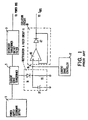
- FIG. 1 illustrates a prior art approach to sensing current in a power supply.
- This prior art system includes a power supply block 3 that typically includes a secondary power supply output circuit.
- a current sense transformer circuit 5 is coupled to the power supply secondary output circuit.
- a secondary transformer filter 9 is coupled to the current sense transformer circuit 5.
- the output of the secondary transformer filter 9 is then coupled to a power bus (e.g., 5V power bus).
- the output of the current sense transformer is a current determined by the transformer's turn ratio.
- a rectification and filter circuit 11 is coupled to the current sense transformer circuit 5 for detecting the output of the current sense transformer circuit 5 and converting the current pulses output into a rectified analog waveform.
- Circuit 11 may be implemented using a diode 31 that is coupled in series with a parallel combination of a resistor 35, and a capacitor 37.
- Resistor 35 determines the voltage sensed at the current peaks since voltage equals the product of the current and the resistance.
- the storage capacitor 15 stores energy during the current off time with a time constant of the resistance of resistor 35 times the capacitance of capacitor 37.
- the output of the transformer is a current pulse with a duty cycle set by the power supply of typically thirty percent (30%), the voltage across resistor 35 and capacitor 37 does not reach a peak voltage value of the current times resistor 35. Also, during the off time, resistor 35 will discharge capacitor 37, which results in a ripple voltage.
- the response to a current step increase is determined by capacitor 37 and the response to a current step decrease is determined by the time constant formed by resistor 35 and capacitor 37. Therefore, this type of detector has limitations in transient response, ripple voltage, and accuracy is affected by the duty cycle of the current pulses, since resistor 35 and capacitor 37 function as an averaging circuit.
- the duty cycle is affected by the load, as well as, the other outputs.
- the output of the storage capacitor 37 is coupled to a sense node (I sense ) 16. Typically, a current share controller 17 may be coupled to the sense node 16.
- a sense bus isolation circuit 19 is coupled to the sense node 16.
- the output of the isolation circuit is typically coupled to the I bus .
- the I bus is a signal bus having a voltage which represents the output current of the power supply.
- the I bus allows the power supplies to adjust their output current to match the largest output current which is represented by the signal on the I bus .
- An isolation circuit 19 typically includes an operational amplifier 45 having an output port that is coupled to a diode 47.
- the negative terminal of the diode is coupled to the negative terminal of the operational amplifier 45 to provide negative feedback.
- the circuit couples a positive I sense signal to the I bus without affecting the sense node 16. As long as the sense node 16 is more positive than the I bus , the rectification circuit will apply the sense node voltage to the I bus .
- the I bus is the current share bus and has the I sense voltage corresponding to the power supply with the highest sense node voltage.
- the peak detection and sample and hold circuit that employs a resistor and capacitor (RC) introduces an RC delay into the current sense operation. This RC delay affects the time before an current sense reading is accurately detectable.
- the prior art circuit for detecting current has no element for preventing and/or minimizing ripples on the sense waveform due to the discharge of the capacitor 37 by the resistor 35.
- an apparatus for sensing current is desirable that minimizes RC delay, maintains accuracy over changing duty cycle, and minimizes ripples in the current sense waveform.
- US-A-4383293 discloses an inverter circuit having an output current sensing circuit for a converter circuit converting between AC and DC using at least one controllable power semiconductor.
- the sensor circuit comprises a resistor 35 across which is developed a voltage indicative of a peak current conductor by power transistors.
- the peak current signal is transmitted to an inverter control circuit to protect the power transistors by limiting the peak current.
- the present invention is a simple, low cost current sense circuit for power supplies that provides very fast transient response and a direct current voltage that accurately represents the actual power supply output current with minimal ripple voltage. Accuracy is not affected by the power supply pulse duty cycle.
- FIG. 2 illustrates a redundant power supply system in which the present invention may be implemented.
- a redundant power supply system typically includes a backplane 61 that includes a plurality of current sense busses (I bus ) 65 and a plurality of power busses 67.
- the sense busses 65 provide a voltage representing the output current of each power supply to the power supplies of the system and to other components in the system.
- each power supply voltage is provided so that the other components may use this current information to regulate and control the power supplies.
- the power busses 67 simply provide the power supply voltages needed by a computer system.
- each of these power supplies provide the required voltages (e.g., 12 volts, 5 volts, 3.3 volts) to the power busses 67 and provide the respective current sense for each of those power supply voltages to the sense busses 65.
- Each power supply has an input for receiving an AC power supply from an AC power source 73.
- Each of the power supplies may also have a plurality of miscellaneous inputs and outputs (e.g., power_good, DC_On_Off, alarm).
- the power supplies typically provide a number of signals (not shown) to the system. These signals indicate to other circuits, disposed on the backplane 61, that a particular power supply has failed, is okay, or is providing good regulation.
- the backplane 61 also includes miscellaneous circuits 69, such as interface and control circuits that interface between the power supplies and the computer system.
- the present invention may be implemented in any of the power supplies (77, 79, 83) and implemented in any number of these power supplies.
- the details of a power supply will be described hereinafter in Figure 3 .
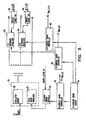
- FIG. 3 illustrates in greater detail a power supply 121 in which the present invention may be implemented.
- a power supply 121 includes an oscillator circuit 125 for generating a frequency at which to switch the power supply.
- a power supply 121 includes a pulse width modulator (PWM) circuit 127 that controls the switching of the power supply.
- PWM pulse width modulator
- a series of secondary regulator circuits e.g., mag amp, line regulators, DC to DC converter
- one for each voltage e.g., 135, 145
- a remote sense circuit (139,149) is coupled to several of the power supply voltages. This remote sense circuit 139 controls the output of the secondary regulator circuit in response to a remote sense signal from the current sense busses.
- the secondary regulator circuit and remote sense circuit combination is used for voltage such as 12 volts and 3.3 volts since the secondary regulator circuit is very efficient.
- This secondary regulator circuit may be any one of several regulator circuits, such as a magnetic amplifier (mag. amp.), linear, or other circuit.
- the optical isolation circuit 173 For the primary voltage (e.g., 5 volts), there is no secondary regulator circuit and the remote sense signal is provided to an optical isolation circuit 173.
- the optical isolation circuit 173 is further coupled to a current share controller 161.
- the current share controller e.g., 161 provides a control signal that increases the voltage of the power supply as required to current share. This control signal is provided to the optical isolation circuit 173.
- a current share controller (165, 168) is coupled to each of the secondary regulator circuit for providing a control signal to increase the voltage of that particular power supply.
- the current share controller may be implemented by an off-the-shelf the parts or by an apparatus described in the above-referenced patent to the common assignee.
- FIG. 4 illustrates in greater detail the current share controller 161.
- the share current controller 161 includes a plurality of comparator control circuits 183.
- Each comparator control circuit includes a first input for receiving an internal current sense (I sense ) voltage that may be provided by the present invention.
- the comparator control circuit includes an output for controlling the output voltage of the power supply and a second input from the I bus voltage.
- the comparator control circuit 183 in response to the difference of the two inputs (i.e., I bus , internal sense), generates a control signal to the mag amp or optical isolation buffer. For example, if a decrease in the internal current is detected with regard to I bus , then the comparator control circuit 183 increases the power supply voltage of that power supply.
- FIG. 5 illustrates a block diagram of one embodiment of the present invention.
- the present invention includes a power supply transformer secondary output circuit 201.
- this circuit 201 may be implemented using a full wave, forward converter, or other configuration. It will be noted by those skilled in the art that the secondary output circuitry 201 may be implemented using a number of different configurations.
- a current sense transformer 205 is coupled to the power supply transformer secondary output circuit 201.
- a secondary output filter 207 is coupled to the current sense transformer 205. The secondary output filter transforms the voltage pulse into a DC voltage.
- the secondary output filter 207 includes an output for providing a power supply voltage to a power bus.
- the current sense transformer 205 simply detects a current from the secondary output circuitry 201.
- the secondary output filter circuit 207 has an input port for receiving a current from the secondary output circuitry 201.
- the peak detection sample and hold circuit 211 is coupled to the current to voltage conversion circuit 206.
- the peak detection sample and hold circuit 211 includes a sample and hold unit and an enable signal generator, hereinafter described.
- the output of the peak detection sample and hold circuitry 211 is coupled to a current share controller 17, described previously and an isolation circuit 219, which rectifies the signal at the I sense node into a current sense voltage for the sense busses (I bus ).
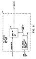
- FIG. 6 illustrates in greater detail the peak detecting sample and hold circuit 211 of one embodiment of the present invention.
- the peak detecting sample and hold circuit 211 of the present invention includes a sample and hold unit 221 for receiving a voltage sensed from the secondary transformer 201 and converting it into a current sense voltage (I sense ).
- the sample and hold unit 221 may be implemented with a transistor, a capacitor, and resistors in one embodiment, as will be described hereinafter.
- the peak detecting sample and hold circuit 211 also includes a sample and hold enable signal generator 225 for generating an enable signal that enables a sample and hold unit 211 to convert the voltage sensed from the output of the conversion circuit 206 into the signal at the I sense node.
- the hold enable signal generator 225 includes a first input for receiving a voltage from the power supply transformer secondary output circuit 201.
- the hold enable signal generator 225 shapes the voltage received from the secondary transformer into an enabling signal.
- This circuit 225 basically provides a slow turn-on and a fast turn-off of the sample and hold unit 221.
- T2 is the main power transformer in a switching power supply.
- T1 is a current sense transformer which has one turn on the primary side (the wire connecting the rectifying diodes D2 and D3 to the output filter consisting of L1 and C1.
- D2, D3, D5, L1, and C1 are the components normally found in a power supply.
- D5 is the catch diode, which clamps the voltage at the input of L1 when D2 and D3 are not conducting.
- the D2 and D3 configuration is shown for a push-pull power supply circuit, but different configurations of D2 and D3 are is equally suitable for other type of converters, such as Forward and Flyback converters.
- the peak current of I1 is equal to the +5V load current Io, plus some ripple current.
- the current out of the current sense transformer is I2, and is equal to I1/N, where N is the number of turns on the secondary of T1.
- I2 develops a voltage across R1.
- I1 goes to zero, the magnetic field in T1 is reset by resistor R5 by the negative voltage across R5 so that the T1 does not saturate.
- Diode D6 isolates this negative voltage from R1 so that the transformer can be reset.
- a positive voltage at the anode of D4 is conducted through R2 to the gate (V2) of a field effect transistor (FET) Q1 to turn it on at the peak current reading of I1.
- FET field effect transistor
- Resistors (R2 and R3) form a voltage divider so that the gate-to-source voltage of Q1 does not exceed its rating.
- D8, R2, R3, and C2 form a delay network so that the turn-on of Q1 is delayed to prevent a turn-on transient of 12 from being applied to C3.
- R6 allows the peak of 12 to be smoothed so that the voltage stored on C3 represents the average peak current of I2.
- This voltage is I sense , and is a DC voltage representation of Io.
- U1 and D10 buffer and isolate I sense so that this voltage may be coupled to a current sense bus for use with current shared power supplies, such as redundant power systems.
- the resistor (R4) and diode (D7) provide a current path to discharge C2 quickly and to turn Q1 off at the end of the I1 conduction.
- Diode D9 damps the gate voltage V2 close to ground.
- the peak current through the secondary transformer, as represented by V1, is stored on C3.
- the sample and hold circuit includes a MOSFET transistor (e.g., a metal oxide semiconductor field effect transistor (MOSFET)).
- MOSFET transistor includes having a first port coupled to a current sense transformer for receiving a voltage that is indicative of the current through the secondary transformer, a second port for providing an output voltage that is indicative of a direct current representation of the peak current in the secondary transformer, and a control port for receiving the control signal.
- the MOSFET transistor selectively couples the first port to the second port in response to the control signal generated by the peak detector circuit.
- the sample and hold circuit further includes a storage capacitor that is coupled to the second port for storing the direct current voltage representation of the peak current through the secondary transformer.
- the direct current voltage representation of the peak current through the secondary transformer at the second port can be used for various purposes (e.g., current limiting or current sharing).
- the second port may be coupled to a current sense bus via a buffering and isolation circuit.
- the current sense bus may be employed in current shared power supplies, such as redundant power systems.
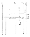
- Waveform 300 is the output of the present invention (i.e., the current sense voltage). Waveform 300 represents a voltage representation of the current provided by this power supply voltage and is simply the voltage at the I sense node. Waveform 304 represents the voltage representation at node V1 of the input current I1.
- the analog waveform 308 represents the voltage (V2) at the gate of transistor Q1.
- the voltage V2 turns Q1 on to allow the current I2 to charge the capacitor C3.
- Q1 is off.
- the resistor-capacitor circuit (R7 and C3) dissipates the voltage stored across C3, so that no voltage is passed to the I Bus .
- the current sense output of the present invention tracks the peak current V1 through the secondary transformer.
- resistor diode and capacitor network (R2, R3, R4, D7, D8, D9 and C2) are used in conjunction with the voltage at the anode of D4 to selectively enable and disable transistor Q1.
- the gate enabling signal is shown as 308 in Figure 8 .
- Figure 9 illustrates the graph of the load current versus time (i.e., at node Io).
- Figure 10 illustrates the sense current versus time.
- Figure 11 illustrates current sense voltage versus time graph of the present invention (i.e., the I sense node).
- the current provided by the power supply voltage ramps up to a peak value of approximately 30 amperes and then falls to approximately 7 to 8 amperes.
- the current sense versus time graph ( Figure 11 ) illustrates that I sense node, which is sampled every ten microseconds, approximates the load current versus time graph.
- the current sense voltage (I sense node) versus time graph also illustrates the voltage across C3 which is based upon the current sense voltage. Note that the I sense voltage ramps to the peak current during the sample period. Also, note that there is negligible voltage drop between the samples.
- the prior art circuits generated a I sense versus time graph as illustrated in Figure 12 .
- the prior art circuit exhibits a slow transient response, as well as, substantial ripple when compared to the present invention.
- the present invention is a simple, low cost current sense circuit for switching power supplies that provides very fast transient response for both increases and decreases in current load. Moreover, the present invention provides a DC voltage that accurately represents the actual power supply output current with minimum ripple. This circuit may be employed in power supplies in current shared, redundant power systems for processors.
Landscapes
- Engineering & Computer Science (AREA)
- Physics & Mathematics (AREA)
- General Physics & Mathematics (AREA)
- Power Engineering (AREA)
- Electromagnetism (AREA)
- Radar, Positioning & Navigation (AREA)
- Automation & Control Theory (AREA)
- Dc-Dc Converters (AREA)
Claims (8)
- Système de bloc d'alimentation comprenant :a. un circuit de sortie secondaire de transformateur d'alimentation (201) ayant un courant passant à travers le transformateur secondaire ;b. un transformateur à détection de courant (205), couplé au circuit de sortie secondaire de transformateur d'alimentation, ledit transformateur à détection de courant générant un courant, ledit courant étant indicatif du courant à travers le transformateur secondaire ;c. un circuit de conversion courant/tension (206) couplé au transformateur à détection de courant (205), pour convertir le courant fourni par le transformateur à détection de courant en une tension, ladite tension représentant le courant à travers le transformateur secondaire ; etd. un circuit échantillonneur bloqueur à détection de crête (221, 225) couplé au circuit de sortie secondaire de transformateur d'alimentation et au circuit de conversion courant/tension, ledit circuit échantillonneur bloqueur à détection de crête fournissant de façon sélective la tension générée par le circuit de conversion courant/tension au niveau d'un noeud de sortie (V1NODE) en réponse à un courant de crête reçu du circuit de sortie secondaire de transformateur d'alimentation, et un circuit bloqueur à détection de crête comprenant un transistor (Q1) et deux résistances (R2, R3) formant un réducteur de tension ; le système de bloc d'alimentation étant caractérisé en ce que ledit circuit bloqueur à détection de crête comprend en outre un réseau à retard comprenant une diode (D8) et un condensateur (C2).
- Système de bloc d'alimentation selon la revendication 1, dans lequel le bloc d'alimentation comprend en outre un circuit d'isolation (173), couplé au circuit échantillonneur bloqueur à détection de crête, ledit circuit d'isolation isolant la sortie du circuit échantillonneur bloqueur à détection de crête d'un bus de détection de courant.
- Système de bloc d'alimentation selon la revendication 1, dans lequel le circuit échantillonneur bloqueur à détection de crête (221, 225) comprend en outre :a. un détecteur de crête, couplé au circuit de sortie secondaire de transformateur d'alimentation, ledit détecteur de crête générant un signal de commande en réponse à une crête venant du circuit de sortie secondaire de transformateur d'alimentation ; etb. une unité échantillonneuse bloqueuse (221), couplée au circuit de conversion courant/tension et au détecteur de crête, pour fournir sélectivement la sortie du circuit de conversion courant/tension à un port de sortie de l'unité échantillonneuse bloqueuse sous la direction du signal de commande.
- Système de bloc d'alimentation selon la revendication 1, dans lequel l'unité échantillonneuse bloqueuse (221) comprend en outre un condensateur (C3) pour stocker une tension, ladite tension représentant le courant à travers le transformateur secondaire.
- Système de bloc d'alimentation selon la revendication 3, dans lequel l'unité échantillonneuse bloqueuse (221) comprend en outre :a. un premier port (S) pour recevoir une tension, ladite tension étant indicative du courant à travers le transformateur secondaire ;b. un second port (D) pour fournir une tension de sortie, ladite tension de sortie étant une représentation de tension de courant direct du courant à travers le transformateur secondaire ; etc. un port de contrôle (G) pour recevoir le signal de commande, ladite unité échantillonneuse bloqueuse couplant sélectivement le premier port au second port en réponse au signal de commande.
- Système de bloc d'alimentation selon la revendication 3, dans lequel le détecteur de crête comprend en outre un circuit de commande, couplé au transformateur secondaire, ledit circuit de commande générant le signal de commande en réponse à l'impulsion de courant de crête.
- Système de bloc d'alimentation selon la revendication 5, dans lequel l'unité échantillonneuse bloqueuse (221) comprend en outre ledit transistor qui est un transistor à effet de champ (Q1), ledit transistor à effet de champ ayant le premier port et le port de commande.
- Système de bloc d'alimentation selon la revendication 7, dans lequel le transistor à effet de champ est un semi-conducteur à oxyde métallique.
Applications Claiming Priority (3)
| Application Number | Priority Date | Filing Date | Title |
|---|---|---|---|
| US633690 | 1990-12-26 | ||
| US08/633,690 US5650715A (en) | 1996-04-19 | 1996-04-19 | Method and apparatus for sensing current in power supplies |
| PCT/US1997/003570 WO1997040437A1 (fr) | 1996-04-19 | 1997-03-11 | Procede et appareil de detection de courant dans les blocs d'alimentation |
Publications (3)
| Publication Number | Publication Date |
|---|---|
| EP0900418A1 EP0900418A1 (fr) | 1999-03-10 |
| EP0900418A4 EP0900418A4 (fr) | 1999-12-22 |
| EP0900418B1 true EP0900418B1 (fr) | 2009-06-24 |
Family
ID=24540713
Family Applications (1)
| Application Number | Title | Priority Date | Filing Date |
|---|---|---|---|
| EP97915881A Expired - Lifetime EP0900418B1 (fr) | 1996-04-19 | 1997-03-11 | Procede et appareil de detection de courant dans les blocs d'alimentation |
Country Status (5)
| Country | Link |
|---|---|
| US (1) | US5650715A (fr) |
| EP (1) | EP0900418B1 (fr) |
| AU (1) | AU2319397A (fr) |
| DE (1) | DE69739471D1 (fr) |
| WO (1) | WO1997040437A1 (fr) |
Families Citing this family (21)
| Publication number | Priority date | Publication date | Assignee | Title |
|---|---|---|---|---|
| US6417653B1 (en) | 1997-04-30 | 2002-07-09 | Intel Corporation | DC-to-DC converter |
| US5874841A (en) * | 1997-07-28 | 1999-02-23 | Philips Electronics North America Corporation | Sample-and-hold circuit for a switched-mode power supply |
| US6011414A (en) * | 1998-02-03 | 2000-01-04 | Philips Electronics North America Corporation | Arrangement for reducing the effects of capacitive coupling in a control circuit for a switched-mode power supply |
| US6066942A (en) * | 1998-05-06 | 2000-05-23 | Intel Corporation | DC-to-DC converter |
| US6069471A (en) * | 1998-05-14 | 2000-05-30 | Intel Corporation | Dynamic set point switching regulator |
| US6140808A (en) | 1998-08-05 | 2000-10-31 | Intel Corporation | DC-to-DC converter with transient suppression |
| US6144115A (en) * | 1998-10-27 | 2000-11-07 | Intel Corporation | Power share distribution system and method |
| US6677687B2 (en) * | 2001-10-23 | 2004-01-13 | Sun Microsystems, Inc. | System for distributing power in CPCI computer architecture |
| US6958596B1 (en) * | 2002-12-20 | 2005-10-25 | Intersil Americas Inc. | Compensation sample and hold for voltage regulator amplifier |
| DE102005006503A1 (de) * | 2005-02-14 | 2006-08-24 | Robert Bosch Gmbh | Verfahren und Schaltungsanordnung zur Erfassung des Stromes eines durch Pulsweitenmodulation gesteuerten Elektromotors |
| US7725753B2 (en) * | 2006-01-13 | 2010-05-25 | Zippy Technology Corp. | Identification apparatus for backup-type power supply systems |
| US8093745B2 (en) * | 2006-07-07 | 2012-01-10 | Ambient Corporation | Sensing current flowing through a power line |
| US20100007315A1 (en) * | 2008-07-09 | 2010-01-14 | Enermax Technology Corporation | High-efficiency power supply device and control method thereof |
| EP2634774B1 (fr) * | 2012-02-28 | 2019-09-18 | Nxp B.V. | Circuit à échantillonnage et maintien et procédé |
| TWI519023B (zh) | 2014-04-03 | 2016-01-21 | 力林科技股份有限公司 | 電源供應裝置 |
| DE102015216481A1 (de) * | 2015-08-28 | 2017-03-02 | Volkswagen Aktiengesellschaft | Wärmetauscher in Plattenbauweise mit Bypass sowie Verfahren zur Herstellung eines Wärmetauschers in Plattenbauweise mit Bypass |
| US10423204B2 (en) | 2017-03-15 | 2019-09-24 | International Business Machines Corporation | Enforcing power caps on computing devices with multiple power feeds |
| US10345888B2 (en) * | 2017-03-15 | 2019-07-09 | International Business Machines Corporation | Power capping for power consumption devices with multiple power supplies |
| JP6584726B2 (ja) * | 2017-05-15 | 2019-10-02 | 三菱電機株式会社 | 電流検出装置 |
| CN111722148B (zh) * | 2020-07-06 | 2023-03-21 | 浙江中控技术股份有限公司 | 一种电流采样电阻电路的故障诊断系统 |
| CN113520521B (zh) * | 2021-08-30 | 2023-11-03 | 江苏朴芃医疗科技有限公司 | 电流峰值检测装置、高压发生器及血管钙化治疗设备 |
Family Cites Families (6)
| Publication number | Priority date | Publication date | Assignee | Title |
|---|---|---|---|---|
| US3768012A (en) * | 1972-05-08 | 1973-10-23 | Pioneer Magnetics Inc | Power supply current detector system |
| US3859586A (en) * | 1973-09-26 | 1975-01-07 | Bell Telephone Labor Inc | Overcurrent protection circuit utilizing peak detection circuit with variable dynamic response |
| US4149233A (en) * | 1977-09-15 | 1979-04-10 | Nasa | Circuit for automatic load sharing in parallel converter modules |
| US4383293A (en) * | 1981-11-16 | 1983-05-10 | Acme Electric Corporation | Isolated DC current sense circuit |
| US5036452A (en) * | 1989-12-28 | 1991-07-30 | At&T Bell Laboratories | Current sharing control with limited output voltage range for paralleled power converters |
| US5508606A (en) * | 1994-04-25 | 1996-04-16 | Eaton Corporation | Direct current sensor |
-
1996
- 1996-04-19 US US08/633,690 patent/US5650715A/en not_active Expired - Lifetime
-
1997
- 1997-03-11 AU AU23193/97A patent/AU2319397A/en not_active Abandoned
- 1997-03-11 WO PCT/US1997/003570 patent/WO1997040437A1/fr not_active Ceased
- 1997-03-11 DE DE69739471T patent/DE69739471D1/de not_active Expired - Lifetime
- 1997-03-11 EP EP97915881A patent/EP0900418B1/fr not_active Expired - Lifetime
Also Published As
| Publication number | Publication date |
|---|---|
| EP0900418A1 (fr) | 1999-03-10 |
| EP0900418A4 (fr) | 1999-12-22 |
| WO1997040437A1 (fr) | 1997-10-30 |
| US5650715A (en) | 1997-07-22 |
| DE69739471D1 (de) | 2009-08-06 |
| AU2319397A (en) | 1997-11-12 |
Similar Documents
| Publication | Publication Date | Title |
|---|---|---|
| US5650715A (en) | Method and apparatus for sensing current in power supplies | |
| US5233287A (en) | Current limiting bilateral converter having a ground referenced current sensor | |
| US6343026B1 (en) | Current limit circuit for interleaved converters | |
| EP0582814B1 (fr) | Circuit pour l'élémination de pertubations | |
| US7208883B2 (en) | Current detection circuit, and power supply apparatus, power supply system and electronic apparatus using the current detection circuit | |
| US6980441B2 (en) | Circuit and method for controlling a synchronous rectifier in a power converter | |
| US9837917B1 (en) | X-cap. discharge method for flyback converter | |
| US6462525B1 (en) | Polyphase PWM converter with high efficiency at light loads | |
| US7443700B2 (en) | On-time control for constant current mode in a flyback power supply | |
| US5757625A (en) | Switched mode power supply with transformer and feedback via primary winding | |
| EP0675588B1 (fr) | ContrÔle du courant d'entrée tiré par un convertisseur de puissance à découpage | |
| US7561452B2 (en) | Transformer-isolated flyback converters and methods for regulating output current thereof | |
| EP0622889B1 (fr) | Circuit d'alimentation prérégulateur à basse puissance | |
| US6181586B1 (en) | Current-to-voltage converter and associate closed-loop control circuit | |
| EP0593257A2 (fr) | Convertisseur d'amplification | |
| CN116260319B (zh) | 一种功率转换器及用于功率转换器的功率开关控制器 | |
| US4593213A (en) | Current-limited MOSFET switch | |
| EP0995258B1 (fr) | Convertisseur cc-cc a boucle fermee et a barriere unique et procede associe | |
| US6101105A (en) | Apparatus and method for identifying an unregulated DC bus voltage | |
| US6765808B1 (en) | Power converter with cross current sensing | |
| US5627740A (en) | Low dissipation current sensing system for a switched DC power supply | |
| EP0332095B1 (fr) | Alimentation de puissance à découpage | |
| US6366484B1 (en) | Cross current sensing in power conversion | |
| JPS6126304B2 (fr) | ||
| US5986897A (en) | Switched-mode power supply having a circuit arrangement for turning the switching device when a voltage on the switching device is at a minimum |
Legal Events
| Date | Code | Title | Description |
|---|---|---|---|
| PUAI | Public reference made under article 153(3) epc to a published international application that has entered the european phase |
Free format text: ORIGINAL CODE: 0009012 |
|
| 17P | Request for examination filed |
Effective date: 19981027 |
|
| AK | Designated contracting states |
Kind code of ref document: A1 Designated state(s): DE FR GB |
|
| A4 | Supplementary search report drawn up and despatched |
Effective date: 19991109 |
|
| AK | Designated contracting states |
Kind code of ref document: A4 Designated state(s): DE FR GB |
|
| RIC1 | Information provided on ipc code assigned before grant |
Free format text: 6H 02M 3/28 A, 6G 05F 1/40 B, 6G 05F 1/56 B |
|
| 17Q | First examination report despatched |
Effective date: 20021022 |
|
| GRAP | Despatch of communication of intention to grant a patent |
Free format text: ORIGINAL CODE: EPIDOSNIGR1 |
|
| GRAS | Grant fee paid |
Free format text: ORIGINAL CODE: EPIDOSNIGR3 |
|
| GRAA | (expected) grant |
Free format text: ORIGINAL CODE: 0009210 |
|
| AK | Designated contracting states |
Kind code of ref document: B1 Designated state(s): DE FR GB |
|
| REG | Reference to a national code |
Ref country code: GB Ref legal event code: FG4D |
|
| REF | Corresponds to: |
Ref document number: 69739471 Country of ref document: DE Date of ref document: 20090806 Kind code of ref document: P |
|
| PLBE | No opposition filed within time limit |
Free format text: ORIGINAL CODE: 0009261 |
|
| STAA | Information on the status of an ep patent application or granted ep patent |
Free format text: STATUS: NO OPPOSITION FILED WITHIN TIME LIMIT |
|
| 26N | No opposition filed |
Effective date: 20100325 |
|
| REG | Reference to a national code |
Ref country code: FR Ref legal event code: ST Effective date: 20101130 |
|
| PG25 | Lapsed in a contracting state [announced via postgrant information from national office to epo] |
Ref country code: FR Free format text: LAPSE BECAUSE OF NON-PAYMENT OF DUE FEES Effective date: 20100331 |
|
| PGFP | Annual fee paid to national office [announced via postgrant information from national office to epo] |
Ref country code: GB Payment date: 20140305 Year of fee payment: 18 |
|
| PGFP | Annual fee paid to national office [announced via postgrant information from national office to epo] |
Ref country code: DE Payment date: 20140417 Year of fee payment: 18 |
|
| REG | Reference to a national code |
Ref country code: DE Ref legal event code: R119 Ref document number: 69739471 Country of ref document: DE |
|
| GBPC | Gb: european patent ceased through non-payment of renewal fee |
Effective date: 20150311 |
|
| PG25 | Lapsed in a contracting state [announced via postgrant information from national office to epo] |
Ref country code: DE Free format text: LAPSE BECAUSE OF NON-PAYMENT OF DUE FEES Effective date: 20151001 Ref country code: GB Free format text: LAPSE BECAUSE OF NON-PAYMENT OF DUE FEES Effective date: 20150311 |