EP0901080A1 - Arbitrierungssystem - Google Patents
Arbitrierungssystem Download PDFInfo
- Publication number
- EP0901080A1 EP0901080A1 EP98307033A EP98307033A EP0901080A1 EP 0901080 A1 EP0901080 A1 EP 0901080A1 EP 98307033 A EP98307033 A EP 98307033A EP 98307033 A EP98307033 A EP 98307033A EP 0901080 A1 EP0901080 A1 EP 0901080A1
- Authority
- EP
- European Patent Office
- Prior art keywords
- memory
- address
- access
- port
- request
- Prior art date
- Legal status (The legal status is an assumption and is not a legal conclusion. Google has not performed a legal analysis and makes no representation as to the accuracy of the status listed.)
- Granted
Links
Images



Classifications
-
- G—PHYSICS
- G06—COMPUTING OR CALCULATING; COUNTING
- G06F—ELECTRIC DIGITAL DATA PROCESSING
- G06F12/00—Accessing, addressing or allocating within memory systems or architectures
- G06F12/02—Addressing or allocation; Relocation
- G06F12/0215—Addressing or allocation; Relocation with look ahead addressing means
-
- G—PHYSICS
- G06—COMPUTING OR CALCULATING; COUNTING
- G06F—ELECTRIC DIGITAL DATA PROCESSING
- G06F13/00—Interconnection of, or transfer of information or other signals between, memories, input/output devices or central processing units
- G06F13/14—Handling requests for interconnection or transfer
- G06F13/16—Handling requests for interconnection or transfer for access to memory bus
- G06F13/1605—Handling requests for interconnection or transfer for access to memory bus based on arbitration
- G06F13/161—Handling requests for interconnection or transfer for access to memory bus based on arbitration with latency improvement
- G06F13/1626—Handling requests for interconnection or transfer for access to memory bus based on arbitration with latency improvement by reordering requests
- G06F13/1631—Handling requests for interconnection or transfer for access to memory bus based on arbitration with latency improvement by reordering requests through address comparison
Definitions
- the present invention relates to a bus arbitration system and method of controlling memory accesses from multiple memory users.
- FIG. 1 A generalised scenario is illustrated by Figure 1.
- reference numeral 2 denotes a bus arbiter for controlling accesses by a plurality of ports PORT 0 ...PORT 15 to a memory bus 4.
- the memory bus 4 is connected to memory resource via an external memory interface not shown in Figure 1. Alternatively, it could be connected directly to on-chip memory.
- Each port has a memory access path MA 0 ...MA 15 connecting it to the memory bus by which memory addresses can be sent to the memory resource and items returned from the memory resource.
- Each port has a request line r 0 ...r 15 connected to the bus arbiter and a grant line from the bus arbiter to each port g 0 ...g 15 .
- Each port also has a bus_busy line bb 0 ...bb 15 which are connected through an OR gate 6 to the bus arbiter 2.
- Each port signals its request by asserting the request line r 0 ...r 15 . Some time later the arbiter asserts one of the grant lines indicating which port can use the bus. This process is known as "awarding tenure" of the bus.
- On receipt of a grant signal a port asserts its bus_busy signal then uses the memory bus to satisfy one or more of its memory requests via its memory access path MA. When the port is finished it de-asserts the bus_busy signal allowing the arbiter to award tenure again.
- a bus arbitration system comprising:
- an access span is a sequence of requests from a single port to which the arbiter grants tenure consecutively.
- said locations are addressable by memory addresses comprising a number of addressing bits such that locations within an address set are addressable by a reduced number of addressing bits.
- the invention can be used to advantage in any situation where clustering accesses on the basis of locality may ultimately lead to relative addressing (possibly as a side effect using fewer addressing bits). This may be the case in magnetic and optical disks, magnetic tape etc because the clustering implies less disk head/tape transport movement per access.
- the invention is particularly useful in the context of DRAMs having a so-called fast page accessing mode.
- DRAMs are normally addressed by applying a row address and a column address to identify a particular location in memory. Memory addresses that have the same row address are said to be on the same page. If successive accesses are on the same page, the row address does not have to be reapplied so the second and subsequent accesses cost less time.
- each address set constitutes a page in memory and the reduced number of addressing bits address the line in each page.
- the arbiter has sequence determining circuitry for determining the sequence in which memory users are examined by the arbiter to see whether or not they are generating a request.
- This sequence can be programmable to take into account the number and type of memory users having access to the memory bus. This allows any particular architecture to be optimised in terms of its memory access bandwidth and latency requirements.
- the arbitrator can also include timing circuitry for determining a maximum time allowed between consecutive requests in an access span. If this time is exceeded that span will be terminated and a next request from a different memory user will be considered.
- the predetermined number of accesses within each access span for each memory user may also be programmable to take into account the pattern of memory accesses effected by each memory user.
- the invention also provides a method of controlling accesses by multiple memory users to a common memory wherein items are held at locations in memory organised in address sets such that when one location in an address set has been accessed, remaining locations in the same address set can be accessed more quickly by a subsequent memory access than other locations in the memory,
- Modern high-performance DRAM chips (dynamic read only memory chips) have a feature called fast page mode, which means that the most efficient way of using these types of memory occurs when there is a high degree of locality in the addresses being accessed.
- fast page mode a feature called fast page mode
- P log 2 (dram page size)
- the described embodiment of this invention exploits fast page mode by providing a bus arbiter (referred to herein as an arbitrator) which awards tenure in a manner which maximises the likelihood of getting on-page accesses and hence optimises memory performance.
- a bus arbiter referred to herein as an arbitrator
- Figure 2 The approach used is illustrated by Figure 2.
- the bus arbitration scheme includes a bus arbitrator 2 for controlling accesses from a plurality of ports PORT 0 ...PORT 15 to a memory bus 4.
- the memory bus 4 is itself connected to an external memory interface 8 connected to a memory resource such as a DRAM 10.
- Memory access paths, MA, request lines r, grant lines g and bus_busy lines bb are provided as described above with reference to Figure 1.
- each port Along with its request signal r each port generates a signal s 0 ...s 15 called samep. When asserted, the samep signal indicates that any difference between the address of the current request and this port's previous request is confined to the P lower order address bits.
- the arbitrator uses this knowledge of the locality of accesses from each port to determine whether it should service a multiplicity of requests from that port or whether it should move on to service another port's request.
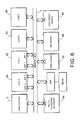
- Figure 8 is a schematic block diagram of circuitry located within each port for generating the same P signal.
- a memory access controller 100 within each port generates a memory access request including a memory address and, if appropriate, associated data.
- the memory address and any data is stored in a buffer 102.
- the most significant 21 address bits are supplied to a comparator 104.
- the comparator also receives the most significant 21 address bits from a preceding address which has been stored in a last packet address store 106.
- the comparator 104 determines that any difference between the address of the current request and the previous request made by the port is confined to the P lower order address bits. If so, the same P signal is asserted by the comparator.
- the port circuitry also includes a bus driver 108 which generates the request and memory access signals and receives the grant signal.
- the arbitrator allocates a maximum number of times that it will consecutively award tenure (each allowing one memory access) to each port. It will continue to award tenure to a port which has its request line asserted and its samep signal asserted so long as this maximum number is not exceeded. It will otherwise award tenure in a modified round-robin manner.
- Figure 3 illustrates arbitration circuitry of a simplified embodiment of the invention.
- Annexe 1 describes the symbols used in Figures 3 and 4.
- Each of the request signals r 0 ...r 15 are supplied to a first multiplexor 12.
- the samep signals s 0 ...s 15 are supplied to a second multiplexor 14. If a request signal is asserted while a particular port is being examined, the multiplexor 12 outputs a signal on request line 16 which is supplied to a first AND gate 26 and to the inverted input of a second AND gate 18 and a third AND gate 20. If a samep signal is asserted while the port is under examination, the second multiplexor 14 supplies a signal along samep line 22 to an input of an OR gate 24.
- a port counter 28 examines the ports in turn via the multiplexors 12,14. Ports are examined in a predetermined sequence, for example port 15 then port 14 and so on until port 0, then port 15 is reexamined. Movement of the port counter from one port to the next is under the control of a decr input 30.
- the decr input 30 is updated by a port-1 signal on line 32 via an OR gate 34 which determines that the port-1 signal is asserted if one of the following three signals is asserted.
- the first of these is the output of the third AND gate 20 on line 36.
- the output of the NOR gate 34 which is used to control the decr input 30 of the port counter 28 is also used to control the set input of an RS flip-flop 46.
- the AND gate 26 generates a grant signal on line 48 which is supplied via a demultiplexor 50 to the port currently being examined.
- the grant signal on line 48 is generated if the request line 16 is asserted and if either the samep line 22 is asserted or the output of the RS flip-flop 46 is asserted on the First line 52. This indicates that the request is the first request made by the port under examination.
- the grant signal on line 48 is supplied to the reset input of the RS flip-flop 46 to deassert the first signal on line 52 after the first memory access has been granted to the port under examination.
- the arbitrator will continue to assert the grant line in accordance with the following parameters:
- the port counter 28 is decremented and the arbitrator starts a new span with a different port in the following conditions:
- the state of the arbitrator at any time is held by the three counter registers: PORT 28, SPAN 44 and PATIENCE 40. In this implementation they have the values shown in TABLE I. Counter name Range Reset value Port 0..15 Don't care Span 0..4 4 Patience 0..6 6
- the value in the PORT counter 28 indicates the port which currently has tenure (i.e. is granted) or the port which is being examined to determine if it has a request.
- the port has initial value 15 and decrements to 0 when its decr line 30 is asserted. On being decremented from 0 it wraps around back to the value 15. In this way each port in turn is visited in a cyclical manner.
- the value in the SPAN counter 44 indicates the number of further requests that a port may be granted. As each request is granted, the grant signal on line 48 causes the span-1 line 54 to be asserted thus decrementing the SPAN counter 44. When a requester has been granted 4 times the port is decremented and a different requester is given the opportunity to be granted. The SPAN counter is reset by the port-1 signal on line 32.
- the patience counter 40 is essentially a timer which can end a span if requests are not made soon enough after the last request in the same span. On starting a new span the patience counter has the value 6. The counter is decremented on each cycle that the bus is not busy and there is no request (by the outputs of the second AND gate 18). It is reset each time a grant is made (grant signal on line 48) or the port counter value changes (port-1 signal on line 32).
- a grant signal is asserted for the examined port if the port indicated by the current value of port counter asserts a request which is either the first in a span or has its samep signal asserted.
- a port Once a port has received a grant it de-asserts its request on the next cycle. When it has another request to make it can do so at any time after the bus_busy cycle is asserted.
- the port asserts its samep signal if the address of the current access differs from that of the previous address in only the lower order 11 bits. This is done by a simple compare circuit in the port which is not described further herein.
- FIG 4 shows an enhanced version of the arbitrator. With reference to the circuit of Figure 3 it makes two enhancements:
- the programmability is achieved by adding a register bank 60 of 32 registers which contains ⁇ port,span ⁇ tuples and a port address register.
- a register controller 62 allows the contents of the registers Reg 0 ...Reg 31 to be accessed responsive to a PORT address supplied on address bus 64.
- the PORT address is supplied from a PORT address counter 66 which receives the port-1 signal output from the OR gate 34.
- the contents of each register are supplied along data bus 68 to the PORT register 29 which takes the place of the PORT counter 28 in Figure 3, as described more fully hereinafter.
- the port-1 signal is also used to generate a read signal on line 70 to activate the register controller 62.
- the PORT address counter 66 is decremented which causes the PORT register and the SPAN register to fetch new values from the register bank 60 at the position pointed at by the PORT address counter.
- the programming also affects the maximum latency observed by a port.
- the maximum latency observed by a port can be calculated by observing the maximum number of requests granted to other ports which can occur between consecutive visits to the same port. By placing several spans belonging to a port in the register bank 60 it is possible to limit this arbitrarily. For example, if all span widths were of value 4, then by programming every other register to contain a span for some port P 3 say, then port P 3 is never more than four memory accesses away from being granted.
- Ports are examined in turn in the order as determined by the contents of the register 31 then register 30 and so on until register 0 then the contents of PS register 31 are re-examined.
- n of a span is determined by the contents of the register for that port.
- requests have to access addresses which differ only in their lower 11 bits (as indicated by samep) and have to be made within 6 cycles of the previous request in this span.
- the state of the arbitrator at any time is held by the four registers constituting the PORT register 29, the PORT address counter 66, the SPAN counter 44 and the PATIENCE counter 40. In this implementation they have the values shown in TABLE II. Register name Range Reset/Reload value Port register 15..0 Reload from PS register Port address counter 31..0 Don't care Span Counter 0..4 Reload from PS register Patience 0..6 Reset to 6
- the value of the PORT address counter 66 determines which register in the register bank 60 will next load its contents ⁇ port,span ⁇ respectively into the port register 29 and span counter 44.
- the decr signal line of this register is decremented by the port-1 signal the values in the register addressed by the contents of the port address counter are loaded into the port register and span counter via the data bus 70.
- the value in the PORT register 29 indicates the port which currently has tenure (i.e. is granted) or the port which is being examined to determine if it has a request.
- the value in the SPAN counter indicates the number of further requests that a port may be granted. This controls generation of the grant signal in a manner described previously.
- the PATIENCE counter is essentially a timer which can terminate a span if requests are not made soon enough after the last request in the same span.
- the patience counter On starting a new span the patience counter has the value 6. The counter is decremented on each cycle that the bus is not busy and there is no request. It is reset each time a grant is made or the port address counter value changes.
- the register bank 60 is a set of 7-bit registers which control the order of traversal of the ports and the size of each span. They are in the memory address space and so are read/writable by a processor or other device which may want to program the arbitrator.
- the mechanism for accessing the register bank by another bus user is standard and not described here.
- Each register has two fields: a 3-bit span field comprising bits 0...2 of each register and a 4-bit port field comprising bits 3...6 of each register. This is shown in Figure 5.
- the register controller 62 accesses the register indicated by the contents of the Addr lines 64 and places the 7-bit contents onto the data bus 68, where the appropriate bits are latched into the port register 29 and span counter 44.
- the grant signal is asserted if the port indicated by the current value of port counter is asserting a request which is either the first in a span or has its samep signal asserted.
- a port Once a port receives a grant it de-asserts its request on the next cycle. When it has another request to make it can do so at any time after the bus_busy cycle is asserted.
- the port asserts its samep signal if the address of the current access differs from that of the previous address in only the lower order 11 bits.
- the ports of the above-referenced modules are each allocated a port number.
- One allocation example is given in TABLE III.
- Module and port name Port number Binary port number Instruction port of CPU0 1 0001 Data port of CPU0 2 0010 Instruction port of CPU1 3 0011 Data port of CPU1 4 0100 Audio interface 5 0101 Video interface 6 0110 Network interface 7 0111 Test Reset Debug module 9 1001 Multi Standard Decoder 10 1010 Preloader 11 1011
- TABLE 4 represents an example of how the register bank 60 may be programmed to control memory accesses by the various modules connected to the bus 4.
- the effect of a programmed arbitration system can be visualised as in the diagram of Figure 7.
- the arbitration circuitry described above can be considered to have a memory resource pointer MRP which is used as an index for the register bank 60 to determine which port is currently able to request the memory resource.
- MRP memory resource pointer
- the MR pointer moves onto the next port. If this port is not requesting the memory resource, the pointer will move on again. Moving on past inactive points may not be instantaneous, but it is not difficult to ensure that any delay caused can usually be hidden by the time taken for the EMI to satisfy the current request.
- this can be visualised in the form of a wheel around which the memory resource pointer MRP rotates dealing with requests from each port in turn.
- the time taken for the memory resource pointer MRP to cycle round and return to the same value is called the MR period.
- the worst case MR period occurs when each port in the table makes the maximum number of allocated samepage requests.
- the worst case MR period would appear to be the total number of requests in the MR table multiplied by the time for a 4-word read request.
- different ports have different patterns of memory access. For example the audio port 84 always uses single word reads whereas the Instruction fetch port (IRF0,IRF1) of the CPUs uses four-word reads.
- each of these requests is not known to the arbiter but the actual time taken to service the requests will depend on the size of the request so this should be taken into account when programming the MR parameters.
- the arbitration systems described above are able to achieve higher levels of memory performance from standard DRAM memory components than existing arbitration schemes.
Landscapes
- Engineering & Computer Science (AREA)
- Theoretical Computer Science (AREA)
- Physics & Mathematics (AREA)
- General Engineering & Computer Science (AREA)
- General Physics & Mathematics (AREA)
- Bus Control (AREA)
Applications Claiming Priority (2)
| Application Number | Priority Date | Filing Date | Title |
|---|---|---|---|
| GBGB9719047.4A GB9719047D0 (en) | 1997-09-08 | 1997-09-08 | Arbitration system |
| GB9719047 | 1997-09-08 |
Publications (2)
| Publication Number | Publication Date |
|---|---|
| EP0901080A1 true EP0901080A1 (de) | 1999-03-10 |
| EP0901080B1 EP0901080B1 (de) | 2005-06-15 |
Family
ID=10818732
Family Applications (1)
| Application Number | Title | Priority Date | Filing Date |
|---|---|---|---|
| EP98307033A Expired - Lifetime EP0901080B1 (de) | 1997-09-08 | 1998-09-02 | Arbitrierungssystem |
Country Status (4)
| Country | Link |
|---|---|
| US (1) | US6301642B1 (de) |
| EP (1) | EP0901080B1 (de) |
| DE (1) | DE69830550D1 (de) |
| GB (1) | GB9719047D0 (de) |
Cited By (2)
| Publication number | Priority date | Publication date | Assignee | Title |
|---|---|---|---|---|
| US6662251B2 (en) * | 2001-03-26 | 2003-12-09 | International Business Machines Corporation | Selective targeting of transactions to devices on a shared bus |
| WO2007067739A1 (en) * | 2005-12-09 | 2007-06-14 | Advanced Micro Devices, Inc. | Memory access request arbitration |
Families Citing this family (15)
| Publication number | Priority date | Publication date | Assignee | Title |
|---|---|---|---|---|
| JP3606852B2 (ja) * | 2001-08-13 | 2005-01-05 | 沖電気工業株式会社 | バス制御システム |
| KR100455396B1 (ko) * | 2002-10-14 | 2004-11-06 | 삼성전자주식회사 | 마스터 블록들의 우선 순위를 결정하는 파라미터 발생회로 및 파라미터 발생 방법. |
| US8539096B2 (en) * | 2003-09-26 | 2013-09-17 | Lsi Corporation | Systems and methods for configuring ports of an SAS domain |
| WO2005059764A1 (en) * | 2003-12-09 | 2005-06-30 | Thomson Licensing | Memory controller |
| JP4055903B2 (ja) * | 2003-12-26 | 2008-03-05 | シャープ株式会社 | バス通信システム |
| US7975086B1 (en) * | 2004-03-08 | 2011-07-05 | Pmc-Sierra Us, Inc. | Apparatus for real-time arbitration between masters and requestors and method for operating the same |
| US7467247B2 (en) * | 2005-10-31 | 2008-12-16 | Hewlett-Packard Development Company, L.P. | Timeouts on accessing a shared resource |
| US20080059672A1 (en) * | 2006-08-30 | 2008-03-06 | Irish John D | Methods and Apparatus for Scheduling Prioritized Commands on a Bus |
| US8904119B2 (en) | 2012-10-31 | 2014-12-02 | Lsi Corporation | Method and structures for performing a migration of a logical volume with a serial attached SCSI expander |
| US9135198B2 (en) | 2012-10-31 | 2015-09-15 | Avago Technologies General Ip (Singapore) Pte Ltd | Methods and structure for serial attached SCSI expanders that self-configure by setting routing attributes of their ports based on SMP requests |
| US8904108B2 (en) | 2012-10-31 | 2014-12-02 | Lsi Corporation | Methods and structure establishing nested Redundant Array of Independent Disks volumes with an expander |
| US8782292B2 (en) | 2012-10-31 | 2014-07-15 | Lsi Corporation | Methods and structure for performing a rebuild of a logical volume with a serial attached SCSI expander |
| US8756345B2 (en) | 2012-10-31 | 2014-06-17 | Lsi Corporation | Methods and structure for managing protection information with a serial attached SCSI expander |
| US11144457B2 (en) * | 2018-02-22 | 2021-10-12 | Netspeed Systems, Inc. | Enhanced page locality in network-on-chip (NoC) architectures |
| KR20220135048A (ko) * | 2021-03-29 | 2022-10-06 | 삼성전자주식회사 | 버스를 통해 자원을 공유하기 위한 장치 및 방법 |
Citations (4)
| Publication number | Priority date | Publication date | Assignee | Title |
|---|---|---|---|---|
| US4623986A (en) * | 1984-02-23 | 1986-11-18 | Texas Instruments Incorporated | Memory access controller having cycle number register for storing the number of column address cycles in a multiple column address/single row address memory access cycle |
| US5193194A (en) * | 1988-10-18 | 1993-03-09 | Motorola, Inc. | Concurrent arbitration system and method for bus control |
| WO1996030838A1 (en) * | 1995-03-31 | 1996-10-03 | Samsung & Electronic, Co. Ltd. | Memory controller which executes read and write commands out of order |
| US5655102A (en) * | 1993-09-29 | 1997-08-05 | Silicon Graphics, Inc. | System and method for piggybacking of read responses on a shared memory multiprocessor bus |
Family Cites Families (5)
| Publication number | Priority date | Publication date | Assignee | Title |
|---|---|---|---|---|
| US5987574A (en) * | 1997-04-30 | 1999-11-16 | Sony Corporation | Bank arbitration for SDRAM memory control |
| US6049855A (en) * | 1997-07-02 | 2000-04-11 | Micron Electronics, Inc. | Segmented memory system employing different interleaving scheme for each different memory segment |
| US5983325A (en) * | 1997-12-09 | 1999-11-09 | Advanced Micro Devices, Inc. | Dataless touch to open a memory page |
| US6052134A (en) * | 1997-12-22 | 2000-04-18 | Compaq Computer Corp. | Memory controller and method for dynamic page management |
| US6052756A (en) * | 1998-01-23 | 2000-04-18 | Oki Electric Industry Co., Ltd. | Memory page management |
-
1997
- 1997-09-08 GB GBGB9719047.4A patent/GB9719047D0/en not_active Ceased
-
1998
- 1998-09-02 EP EP98307033A patent/EP0901080B1/de not_active Expired - Lifetime
- 1998-09-02 DE DE69830550T patent/DE69830550D1/de not_active Expired - Lifetime
- 1998-09-08 US US09/149,272 patent/US6301642B1/en not_active Expired - Lifetime
Patent Citations (4)
| Publication number | Priority date | Publication date | Assignee | Title |
|---|---|---|---|---|
| US4623986A (en) * | 1984-02-23 | 1986-11-18 | Texas Instruments Incorporated | Memory access controller having cycle number register for storing the number of column address cycles in a multiple column address/single row address memory access cycle |
| US5193194A (en) * | 1988-10-18 | 1993-03-09 | Motorola, Inc. | Concurrent arbitration system and method for bus control |
| US5655102A (en) * | 1993-09-29 | 1997-08-05 | Silicon Graphics, Inc. | System and method for piggybacking of read responses on a shared memory multiprocessor bus |
| WO1996030838A1 (en) * | 1995-03-31 | 1996-10-03 | Samsung & Electronic, Co. Ltd. | Memory controller which executes read and write commands out of order |
Non-Patent Citations (1)
| Title |
|---|
| "Fast Data Access of DRAMs by Utilizing a Queued Memory Command Buffer", IBM TECHNICAL DISCLOSURE BULLETIN, vol. 35, no. 7, December 1992 (1992-12-01), NEW YORK, US, pages 63 - 66, XP000332950 * |
Cited By (6)
| Publication number | Priority date | Publication date | Assignee | Title |
|---|---|---|---|---|
| US6662251B2 (en) * | 2001-03-26 | 2003-12-09 | International Business Machines Corporation | Selective targeting of transactions to devices on a shared bus |
| WO2007067739A1 (en) * | 2005-12-09 | 2007-06-14 | Advanced Micro Devices, Inc. | Memory access request arbitration |
| GB2446997A (en) * | 2005-12-09 | 2008-08-27 | Advanced Micro Devices Inc | Memory access request arbitration |
| US7426621B2 (en) | 2005-12-09 | 2008-09-16 | Advanced Micro Devices, Inc. | Memory access request arbitration |
| GB2446997B (en) * | 2005-12-09 | 2010-11-10 | Advanced Micro Devices Inc | Memory access request arbitration |
| CN101326504B (zh) * | 2005-12-09 | 2012-04-25 | 格罗方德半导体公司 | 存储器访问请求仲裁 |
Also Published As
| Publication number | Publication date |
|---|---|
| US6301642B1 (en) | 2001-10-09 |
| EP0901080B1 (de) | 2005-06-15 |
| DE69830550D1 (de) | 2005-07-21 |
| GB9719047D0 (en) | 1997-11-12 |
Similar Documents
| Publication | Publication Date | Title |
|---|---|---|
| EP0901080B1 (de) | Arbitrierungssystem | |
| KR100420707B1 (ko) | 가변폭버스의동시적인액세스를이용하는다중프로세서시스템에서버스중재를위한방법및시스템 | |
| US6393506B1 (en) | Virtual channel bus and system architecture | |
| KR100420706B1 (ko) | 가변폭버스의동시적인액세스를이용하는다중프로세서시스템에서i/o제어를위한방법및시스템 | |
| US6026464A (en) | Memory control system and method utilizing distributed memory controllers for multibank memory | |
| US6330645B1 (en) | Multi-stream coherent memory controller apparatus and method | |
| US7222224B2 (en) | System and method for improving performance in computer memory systems supporting multiple memory access latencies | |
| EP0625753B1 (de) | Dynamisch programmierbarer Busarbiter mit Einrichtung zur historischen Rückmeldung | |
| EP4315015B1 (de) | Schreibbankgruppenmaske während der arbitrierung | |
| EP4359903B1 (de) | Effiziente rangumschaltung in einer speichersteuerung mit mehreren rangen | |
| KR100296718B1 (ko) | 다중프로세서 시스템에서 가변폭 버스를 동시에 액세스하기 위한 방법 및 시스템 | |
| US12073114B2 (en) | Stacked command queue | |
| KR20010081016A (ko) | 다른 시간에서의 메모리 접근 실행 시 데이터 버스 상의데이터 충돌 감지 장치 및 방법 | |
| US11995008B2 (en) | Memory controller with hybrid DRAM/persistent memory channel arbitration | |
| US11625352B2 (en) | DRAM command streak management | |
| EP4315013B1 (de) | Verwaltung der effizienz von dram-befehlsstreifen | |
| US6928525B1 (en) | Per cache line semaphore for cache access arbitration | |
| EP4150468A1 (de) | Effiziente speicherbusverwaltung | |
| KR20010086034A (ko) | 범용 리소스 접근 제어기 | |
| JP3260456B2 (ja) | コンピュータシステムおよびそれに適した集積回路並びに要求選択回路 | |
| US6202137B1 (en) | Method and apparatus of arbitrating requests to a multi-banked memory using bank selects | |
| US6944698B2 (en) | Method and apparatus for providing bus arbitrations in a data processing system |
Legal Events
| Date | Code | Title | Description |
|---|---|---|---|
| PUAI | Public reference made under article 153(3) epc to a published international application that has entered the european phase |
Free format text: ORIGINAL CODE: 0009012 |
|
| AK | Designated contracting states |
Kind code of ref document: A1 Designated state(s): DE FR GB IT |
|
| AX | Request for extension of the european patent |
Free format text: AL;LT;LV;MK;RO;SI |
|
| 17P | Request for examination filed |
Effective date: 19990902 |
|
| AKX | Designation fees paid |
Free format text: DE FR GB IT |
|
| 17Q | First examination report despatched |
Effective date: 20040212 |
|
| GRAP | Despatch of communication of intention to grant a patent |
Free format text: ORIGINAL CODE: EPIDOSNIGR1 |
|
| GRAS | Grant fee paid |
Free format text: ORIGINAL CODE: EPIDOSNIGR3 |
|
| GRAA | (expected) grant |
Free format text: ORIGINAL CODE: 0009210 |
|
| AK | Designated contracting states |
Kind code of ref document: B1 Designated state(s): DE FR GB IT |
|
| PG25 | Lapsed in a contracting state [announced via postgrant information from national office to epo] |
Ref country code: IT Free format text: LAPSE BECAUSE OF FAILURE TO SUBMIT A TRANSLATION OF THE DESCRIPTION OR TO PAY THE FEE WITHIN THE PRESCRIBED TIME-LIMIT;WARNING: LAPSES OF ITALIAN PATENTS WITH EFFECTIVE DATE BEFORE 2007 MAY HAVE OCCURRED AT ANY TIME BEFORE 2007. THE CORRECT EFFECTIVE DATE MAY BE DIFFERENT FROM THE ONE RECORDED. Effective date: 20050615 |
|
| REG | Reference to a national code |
Ref country code: GB Ref legal event code: FG4D |
|
| REF | Corresponds to: |
Ref document number: 69830550 Country of ref document: DE Date of ref document: 20050721 Kind code of ref document: P |
|
| PGFP | Annual fee paid to national office [announced via postgrant information from national office to epo] |
Ref country code: DE Payment date: 20050825 Year of fee payment: 8 |
|
| PG25 | Lapsed in a contracting state [announced via postgrant information from national office to epo] |
Ref country code: DE Free format text: LAPSE BECAUSE OF FAILURE TO SUBMIT A TRANSLATION OF THE DESCRIPTION OR TO PAY THE FEE WITHIN THE PRESCRIBED TIME-LIMIT Effective date: 20050916 |
|
| ET | Fr: translation filed | ||
| PLBE | No opposition filed within time limit |
Free format text: ORIGINAL CODE: 0009261 |
|
| STAA | Information on the status of an ep patent application or granted ep patent |
Free format text: STATUS: NO OPPOSITION FILED WITHIN TIME LIMIT |
|
| 26N | No opposition filed |
Effective date: 20060316 |
|
| PGFP | Annual fee paid to national office [announced via postgrant information from national office to epo] |
Ref country code: GB Payment date: 20060831 Year of fee payment: 9 |
|
| GBPC | Gb: european patent ceased through non-payment of renewal fee |
Effective date: 20070902 |
|
| REG | Reference to a national code |
Ref country code: FR Ref legal event code: ST Effective date: 20080531 |
|
| PG25 | Lapsed in a contracting state [announced via postgrant information from national office to epo] |
Ref country code: FR Free format text: LAPSE BECAUSE OF NON-PAYMENT OF DUE FEES Effective date: 20071001 |
|
| PGFP | Annual fee paid to national office [announced via postgrant information from national office to epo] |
Ref country code: FR Payment date: 20060928 Year of fee payment: 9 |
|
| PG25 | Lapsed in a contracting state [announced via postgrant information from national office to epo] |
Ref country code: GB Free format text: LAPSE BECAUSE OF NON-PAYMENT OF DUE FEES Effective date: 20070902 |