EP0902512A2 - Integrierte interferometrische Struktur - Google Patents
Integrierte interferometrische Struktur Download PDFInfo
- Publication number
- EP0902512A2 EP0902512A2 EP98402199A EP98402199A EP0902512A2 EP 0902512 A2 EP0902512 A2 EP 0902512A2 EP 98402199 A EP98402199 A EP 98402199A EP 98402199 A EP98402199 A EP 98402199A EP 0902512 A2 EP0902512 A2 EP 0902512A2
- Authority
- EP
- European Patent Office
- Prior art keywords
- amplifier
- output
- optical
- signal
- amplifiers
- Prior art date
- Legal status (The legal status is an assumption and is not a legal conclusion. Google has not performed a legal analysis and makes no representation as to the accuracy of the status listed.)
- Withdrawn
Links
Images


Classifications
-
- H—ELECTRICITY
- H01—ELECTRIC ELEMENTS
- H01S—DEVICES USING THE PROCESS OF LIGHT AMPLIFICATION BY STIMULATED EMISSION OF RADIATION [LASER] TO AMPLIFY OR GENERATE LIGHT; DEVICES USING STIMULATED EMISSION OF ELECTROMAGNETIC RADIATION IN WAVE RANGES OTHER THAN OPTICAL
- H01S5/00—Semiconductor lasers
- H01S5/50—Amplifier structures not provided for in groups H01S5/02 - H01S5/30
-
- G—PHYSICS
- G02—OPTICS
- G02F—OPTICAL DEVICES OR ARRANGEMENTS FOR THE CONTROL OF LIGHT BY MODIFICATION OF THE OPTICAL PROPERTIES OF THE MEDIA OF THE ELEMENTS INVOLVED THEREIN; NON-LINEAR OPTICS; FREQUENCY-CHANGING OF LIGHT; OPTICAL LOGIC ELEMENTS; OPTICAL ANALOGUE/DIGITAL CONVERTERS
- G02F1/00—Devices or arrangements for the control of the intensity, colour, phase, polarisation or direction of light arriving from an independent light source, e.g. switching, gating or modulating; Non-linear optics
- G02F1/35—Non-linear optics
- G02F1/3515—All-optical modulation, gating, switching, e.g. control of a light beam by another light beam
- G02F1/3517—All-optical modulation, gating, switching, e.g. control of a light beam by another light beam using an interferometer
-
- G—PHYSICS
- G02—OPTICS
- G02F—OPTICAL DEVICES OR ARRANGEMENTS FOR THE CONTROL OF LIGHT BY MODIFICATION OF THE OPTICAL PROPERTIES OF THE MEDIA OF THE ELEMENTS INVOLVED THEREIN; NON-LINEAR OPTICS; FREQUENCY-CHANGING OF LIGHT; OPTICAL LOGIC ELEMENTS; OPTICAL ANALOGUE/DIGITAL CONVERTERS
- G02F1/00—Devices or arrangements for the control of the intensity, colour, phase, polarisation or direction of light arriving from an independent light source, e.g. switching, gating or modulating; Non-linear optics
- G02F1/01—Devices or arrangements for the control of the intensity, colour, phase, polarisation or direction of light arriving from an independent light source, e.g. switching, gating or modulating; Non-linear optics for the control of the intensity, phase, polarisation or colour
- G02F1/21—Devices or arrangements for the control of the intensity, colour, phase, polarisation or direction of light arriving from an independent light source, e.g. switching, gating or modulating; Non-linear optics for the control of the intensity, phase, polarisation or colour by interference
- G02F1/225—Devices or arrangements for the control of the intensity, colour, phase, polarisation or direction of light arriving from an independent light source, e.g. switching, gating or modulating; Non-linear optics for the control of the intensity, phase, polarisation or colour by interference in an optical waveguide structure
- G02F1/2257—Devices or arrangements for the control of the intensity, colour, phase, polarisation or direction of light arriving from an independent light source, e.g. switching, gating or modulating; Non-linear optics for the control of the intensity, phase, polarisation or colour by interference in an optical waveguide structure the optical waveguides being made of semiconducting material
-
- H—ELECTRICITY
- H01—ELECTRIC ELEMENTS
- H01S—DEVICES USING THE PROCESS OF LIGHT AMPLIFICATION BY STIMULATED EMISSION OF RADIATION [LASER] TO AMPLIFY OR GENERATE LIGHT; DEVICES USING STIMULATED EMISSION OF ELECTROMAGNETIC RADIATION IN WAVE RANGES OTHER THAN OPTICAL
- H01S5/00—Semiconductor lasers
- H01S5/02—Structural details or components not essential to laser action
- H01S5/026—Monolithically integrated components, e.g. waveguides, monitoring photo-detectors, drivers
-
- H—ELECTRICITY
- H01—ELECTRIC ELEMENTS
- H01S—DEVICES USING THE PROCESS OF LIGHT AMPLIFICATION BY STIMULATED EMISSION OF RADIATION [LASER] TO AMPLIFY OR GENERATE LIGHT; DEVICES USING STIMULATED EMISSION OF ELECTROMAGNETIC RADIATION IN WAVE RANGES OTHER THAN OPTICAL
- H01S5/00—Semiconductor lasers
- H01S5/06—Arrangements for controlling the laser output parameters, e.g. by operating on the active medium
- H01S5/0601—Arrangements for controlling the laser output parameters, e.g. by operating on the active medium comprising an absorbing region
-
- H—ELECTRICITY
- H01—ELECTRIC ELEMENTS
- H01S—DEVICES USING THE PROCESS OF LIGHT AMPLIFICATION BY STIMULATED EMISSION OF RADIATION [LASER] TO AMPLIFY OR GENERATE LIGHT; DEVICES USING STIMULATED EMISSION OF ELECTROMAGNETIC RADIATION IN WAVE RANGES OTHER THAN OPTICAL
- H01S5/00—Semiconductor lasers
- H01S5/10—Construction or shape of the optical resonator, e.g. extended or external cavity, coupled cavities, bent-guide, varying width, thickness or composition of the active region
- H01S5/1003—Waveguide having a modified shape along the axis, e.g. branched, curved, tapered, voids
Definitions
- the invention relates to systems optoelectronics used for optical transmission or the processing of optical digital data.
- the converters of wavelength are used to convert an optical signal transmitted, from one wavelength to another wavelength, while maintaining its performance.
- the information is under the form of binary data represented by pulses modulating an optical carrier wave.
- a binary value is therefore determined according to the level of amplitude (or power) of the modulated optical wave.
- this signal may be subject to degradations that make it more difficult, in terms of receivers, detecting high and low signal levels received.
- the quality of a signal optics is usually defined by at least two parameters: signal-to-noise ratio and rate of extinction.
- the signal-to-noise ratio is defined as the ratio from optical signal power to noise power in a wavelength band containing the length wave of the signal carrier.
- the extinction rate is defined as the ratio of powers corresponding respectively to the high levels and signal down. This rate must be high enough despite variations in the input signal.
- An interferometric structure is shown in Figure 1 in the case of the wavelength converter. It consists of two guiding branches 1 and 2. At least one of these branches is provided with an OA semiconductor optical amplifier 1 . However, in general it is preferable to place a second semiconductor optical amplifier OA 2 on the other branch 2 for reasons of symmetry. Indeed, the presence of the second OA 2 semiconductor optical amplifier makes it possible to conserve substantially the same level of amplification in the two branches of the structure and consequently to have substantially identical powers at the output of the branches of the interferometer.
- optical amplifiers OA 1 , OA 2 are sufficient to form the interferometric structure when it is of the "active-passive" type, that is to say when the guides which compose it are produced from two types of material, for train active guides and passive guides.
- the guides located at the ends of the interferometric structure form passive guides and are made of a non-absorbent material so that the optical signal at the output of the interferometric structure is identical to the signal from the amplifiers OA 1 and OA 2 .
- the realization of such an integrated structure of the “active-passive” type is very complicated to implement because it requires several successive epitaxy recoveries to deposit the two types of material. The realization of this structure being long and tedious, its cost is considerably increased.
- all active that is to say a structure whose guides are all active and formed from a single material.
- the optical signal from the amplifiers OA 1 and OA 2 is strongly absorbed by the material used and the optical power at the output of the structure becomes far too weak to be detected. Consequently, in such an “all active” type structure, it is necessary to place peripheral optical amplifiers in order to amplify the optical power absorbed and to recover a suitable signal at the output of the structure.
- peripheral amplifiers are referenced OA 3 , OA 4 , OA 5 and OA 6 in Figure 1.
- a first coupler K 1 makes it possible to couple one end of each of these branches to a peripheral semiconductor optical amplifier, also called input amplifier OA 5 .
- a laser source 7 also makes it possible to supply, to this peripheral amplifier OA 5 , an output carrier wave M of wavelength ⁇ S.
- a second coupler K 2 is arranged so as to couple the other end of the first branch 1 to another optical semiconductor input peripheral amplifier OA 4 .
- This coupler K 2 allows the introduction into the first amplifier OA 1 of an input signal E of wavelength ⁇ e having been amplified by the input amplifier OA 4 .
- the amplifier OA 1 saturates and the state of the interferometer is changed, which causes a phase modulation of the output carrier wave.
- the waves AM 1 and AM 2 correspond to the waves M 1 and M 2 coming from the coupler K 1 and amplified respectively by the amplifiers OA 1 and OA 2 .
- the output signal S is then amplified by the peripheral output amplifier OA 3 .
- Another peripheral amplifier OA 6 is also provided to respect the symmetry of the structure and to allow the replacement of one of the amplifiers OA 3 or OA 4 in the event of a possible failure.
- the saturation power threshold of the amplifiers OA 1 and OA 2 located in the branches 1 and 2 of such an interferometric structure is set relatively low. Consequently, when the interference of the waves AM 1 and AM 2 is constructive, that is to say when the waves AM 1 and AM 2 are in phase, the optical powers of the two amplifiers OA 1 and OA 2 are added so well that the optical power in the output amplifier OA 3 is very high.
- the output amplifier OA 3 strongly saturates and the extinction rate is very degraded.
- the gain of the high levels becomes lower than the gain of the low levels, so that the output signal S undergoes compression of the high levels and is consequently distorted.
- This deformation can also occur on the input signal E, or on the output carrier wave M. Or, if the input signal E is deformed, or if the output carrier wave M is deformed, then the output signal S is also degraded and the rate of extinction of the interferometric structure is reduced.
- the saturation power input of an amplifier is defined by the power input optics for which the amplifier gain is divided by 2.
- the aforementioned drawbacks may appear in any "all active" interferometric structure.
- the object of the invention is to remedy these drawbacks by proposing a structure which, compared to structures known, makes the input saturation power of peripheral amplifiers more difficult to reach by the input power of these amplifiers. For that, we can either seek to increase the saturation power input of said amplifiers either do so that the input power of these amplifiers is scaled down.
- a structure interferometric integrated to provide an optical signal of output in which a first and a second branch, comprising at least a first semiconductor optical amplifier, are coupled to optical amplifiers input and / or output peripheral semiconductors, characterized in that said structure has a section attenuation between the output of at least one amplifier semiconductor optics of one of the branches and the input of the peripheral output amplifier and / or the length of the waveguide of at least one peripheral amplifier is less than 300 ⁇ m.
- the attenuation section brings at least 50% losses optical.
- the optical semiconductor amplifiers OA 1 and OA 2 situated on the branches of the interferometers of the Mach-Zehnder type or equivalent must have a relatively low saturation threshold.
- the peripheral amplifiers OA 3 should be , OA 4 and OA 5 operate in the lowest saturation regime possible.
- the structure must be such that the input saturation threshold is more difficult to reach by the input power.
- the operating conditions of at least one peripheral amplifier are modified. These operating conditions include the optical power at the input of the amplifier or its input saturation power. Preferably, it is the operating conditions of the output amplifier that are first modified. The operating conditions of the other peripheral amplifiers OA 4 then OA 5 can then be modified to avoid any distortion of the input signal E of the output carrier wave M.
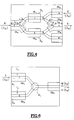
- a first embodiment of a wavelength converter according to the invention consists in enabling the optical power injected into the peripheral output amplifier OA 3 to be reduced.
- This first embodiment is illustrated in the diagram in FIG. 2 which represents a wavelength converter comprising an interferometric structure of the Mach-Zehnder type.
- this converter includes an attenuation section 10, shown in hatched lines in FIG. 2, located between the output of the optical amplifier OA 1 of the first branch 1 and the input of the peripheral output amplifier OA 3 .
- the position of the input of the output amplifier OA 3 is defined as being located just behind the coupler K 3 and not at the limit of the electrode E 3 .
- the attenuation section 10 is obtained by introducing optical losses in the corresponding guide arm 11 wave.
- the waveguide arm 11 can for example be interrupted to diffract part of the light.
- the guide has for example two sections tapered opposite each other, which allows diffract part of the light power and reinject another part. This case is the simplest to realize because only the shape of the mask used to make the engraving of the waveguide changes.
- Another method for introducing these losses consists, for example, in bending the arm 11 of the guide, relative to the end of the amplifier OA 1 , along a steeper slope.
- the losses can also be introduced only at the level of the coupler K 3 by using for example a coupler badly adapted to the interferometric structure.
- the attenuation section can also be produced between the output of the two amplifiers OA 1 , OA 2 and the input of the output amplifier OA 3 , along the guide arms 11 and 12 d 'wave.
- the goal is to get a power level Ps output from the constant converter without damaging the TE extinction rate or S / N signal-to-noise ratio.
- the structure of the attenuation section is such that it allows a contribution of at least 50% of optical losses.
- the attenuation section 10 in the arms 11 and 12, located between the output of the amplifiers OA 1 and OA 2 respectively and the input of the output amplifier OA 3 provides at least 50% of losses optics in each arm 11 and 12 to make it possible to reduce by a factor of 2 the total optical power in the coupler K 3 , that is to say the power injected into the output amplifier OA 3 .
- a second embodiment of a converter wavelength according to the invention consists in increasing the saturation threshold of at least one amplifier peripheral. For this, the structure of the active waveguide of this peripheral amplifier is changed.
- the structure of the guide of the output amplifier OA 3 which is priority modified to maintain a good rate of extinction of the output signal S, and thus to avoid any distortion of this signal.
- the structure of the other peripheral input amplifiers OA 4 then OA 5 can then be modified in order to avoid any distortion of the input signal E and of the output carrier wave M.
- the second embodiment is illustrated in the diagram in FIG. 4 which represents a wavelength converter comprising an interferometric structure of the Mach-Zehnder type in which the length of the active guides of the peripheral amplifiers for output OA 3 and input OA 4 and OA 5 is less than a determined limit value.
- the input saturation power of a semiconductor optical amplifier varies inversely with the length of the active guide of this amplifier. Consequently, to increase the saturation power of the peripheral amplifiers, and in particular that of the output amplifier OA 3 , the length of their active guide is restricted.
- the degradation of the extinction rate occurs essentially in the output amplifier OA 3 , after the coupler K 3 , but also at the output of the input amplifiers OA 4 and OA 5 , before the couplers K 2 and K 1 .
- This degradation of the extinction rate increases with the length of the active waveguide of these amplifiers because the associated saturation power decreases.
- the length of the active guide of a peripheral amplifier is defined as being the length L2 of the guide portion located at the ends of the converter, that is to say between a coupler K 3 or K 1 and the output or l entry of the interferometric structure.
- the length L1 of the first portion of the active guide, of the output amplifier OA 3 which is located before the junction Y, that is to say before the coupler K 3 , is less important.
- the converted signal AM 1 has not yet interfered with the signal AM 2 supplied by the second amplifier OA 2 of the interferometer and is still modulated in phase: the saturation of the amplifier OA 3 output therefore does not modify, in this guide portion, the signal extinction rate. Consequently, the length L1 of the guide portion preceding the coupler K 3 is not restricted.
- the saturation power of the output amplifier OA 3 becomes too weak to allow the interferometer to operate at a suitable output power Ps and with a signal to noise ratio S / B and an extinction rate TE not degraded.
- This limit value of the length L2 of the guide of the peripheral amplifier is equal to 300 ⁇ m.
- the curves of FIGS. 5A to 5C make it possible to compare the results obtained from a peripheral amplifier, for example the output amplifier OA 3 , in which the length L2 of the ribbon of active layer is respectively equal to and less than 300 ⁇ m.
- the overall length L of the compared amplifier remains identical. Indeed, in both cases, the sum of the length L2 of the guide portion located after the coupler K 3 and the length L1 of the guide portion located before this coupler is identical and equal, in the example illustrated on Figures 5A to 5C, at 600 ⁇ m.
- the degradation of the TE extinction rate is greater than 1 or even 2 dB when the length of the amplifier is 300 ⁇ m, while it remains strictly below 1dB when the length of the amplifier is 150 ⁇ m.
- the length of the active waveguide at least at least one peripheral amplifier is preferably less than 300 ⁇ m in order to increase the saturation threshold of this amplifier and maintain a rate of extinction optimum while maintaining an output power Ps suitable.
- the length of the active waveguide must however be both long enough to allow filtration high order optical modes and good quality of the interferometer, and short enough to avoid the effects of signal saturation. Through therefore, this length is preferably between 100 and 300 ⁇ m.
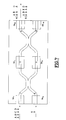
- FIG. 6 represents another structure of Michelson type equivalent to the previous one to which the invention applies.
- the two amplifiers OA 1 and OA 2 are coupled by only one of their ends, the opposite faces being provided with a reflective coating R1, R2.
- the modulating input signal E is injected into the first amplifier OA 1 via the face R1 and the output carrier wave M is injected into the two amplifiers OA 1 and OA 2 by the faces opposite to the faces R1 and R2, via a coupler K1 making it possible to couple one end of each of the branches 1 and 2 to a peripheral semiconductor optical amplifier OA 5 .
- An output signal S, of wavelength ⁇ S resulting from the coupling of auxiliary waves supplied by the first and second amplifiers OA 1 and OA 2 , is then amplified by the peripheral amplifier OA 5 .
- FIG. 7 represents another type of interferometric structure to which the invention applies.
- This type of structure concerns interferometric insertion-extraction multiplexers.
- the structure shown in Figure 7 corresponds to an "all active" device and includes peripheral amplifiers OA 7 , OA 8 , OA 9 , OA 10 at its ends.
- a multiplexed signal with 4 channels ABCD for example is injected into the amplifier referenced OA 7 .
- This signal is separated into two in branches 1 and 2 of the interferometer then recomposed and recovered at the output of the amplifier OA 9 .
- One of the signal channels, for example channel C can be suppressed by sending a control pulse by the amplifier OA 9 to phase-shift the pulses of the channel C in question.
- the signal recovered at the output of the amplifier OA 9 corresponds to the case referenced a) in FIG. 7 and now only includes 3 ABD channels. In the same way, one can then add another X channel by the amplifier OA 8 . In this case, referenced b) in FIG. 7, a multiplexed signal comprising 4 ABXD channels is recovered at the output of the amplifier OA 9 .
Landscapes
- Physics & Mathematics (AREA)
- Nonlinear Science (AREA)
- General Physics & Mathematics (AREA)
- Optics & Photonics (AREA)
- Condensed Matter Physics & Semiconductors (AREA)
- Electromagnetism (AREA)
- Optical Modulation, Optical Deflection, Nonlinear Optics, Optical Demodulation, Optical Logic Elements (AREA)
- Optical Integrated Circuits (AREA)
Applications Claiming Priority (3)
| Application Number | Priority Date | Filing Date | Title |
|---|---|---|---|
| FR9711122A FR2768231B1 (fr) | 1997-09-08 | 1997-09-08 | Structure interferometrique integree |
| FR9711122 | 1997-09-08 | ||
| US09/148,187 US6035078A (en) | 1997-09-08 | 1998-09-04 | Integrated interferometer structure |
Publications (2)
| Publication Number | Publication Date |
|---|---|
| EP0902512A2 true EP0902512A2 (de) | 1999-03-17 |
| EP0902512A3 EP0902512A3 (de) | 1999-05-19 |
Family
ID=26233791
Family Applications (1)
| Application Number | Title | Priority Date | Filing Date |
|---|---|---|---|
| EP98402199A Withdrawn EP0902512A3 (de) | 1997-09-08 | 1998-09-07 | Integrierte interferometrische Struktur |
Country Status (5)
| Country | Link |
|---|---|
| US (1) | US6035078A (de) |
| EP (1) | EP0902512A3 (de) |
| JP (1) | JPH11142902A (de) |
| CA (1) | CA2243858A1 (de) |
| FR (1) | FR2768231B1 (de) |
Families Citing this family (12)
| Publication number | Priority date | Publication date | Assignee | Title |
|---|---|---|---|---|
| FR2781322B1 (fr) * | 1998-07-20 | 2000-09-08 | Alsthom Cge Alcatel | Dispositif d'emission de donnees optiques |
| FR2786279B1 (fr) * | 1998-11-24 | 2000-12-29 | Cit Alcatel | Composant optique a base d'amplificateurs optiques a semi-conducteur comportant un nombre reduit d'electrodes independantes |
| JP2001147409A (ja) | 1999-11-19 | 2001-05-29 | Ddi Corp | 光信号処理装置 |
| GB0007549D0 (en) * | 2000-03-28 | 2000-05-17 | Iltron Limited | A wavelength converter |
| US6563621B2 (en) * | 2000-10-06 | 2003-05-13 | Alphion Corporation | Bit-rate and format insensitive all-optical clock extraction circuit |
| US6570697B2 (en) * | 2000-10-06 | 2003-05-27 | Alphion Corporation | Format insensitive and bit rate independent optical preprocessor |
| US6646773B2 (en) | 2001-05-23 | 2003-11-11 | Board Of Regents, The University Of Texas System | Digital micro-mirror holographic projection |
| US20030068114A1 (en) * | 2001-08-02 | 2003-04-10 | Gayle Link | Semiconductor waveguide optical regenerative device |
| US6856751B2 (en) * | 2002-03-22 | 2005-02-15 | Lynx Photonic Networks, Inc. | Method and system for obtaining variable optical attenuation with very low polarization dependent loss over an ultra wide dynamic range |
| US6879738B2 (en) * | 2003-02-24 | 2005-04-12 | Intel Corporation | Method and apparatus for modulating an optical beam in an optical device |
| WO2006011262A1 (ja) * | 2004-07-30 | 2006-02-02 | Nihon Yamamura Glass Co., Ltd. | 光信号増幅3端子装置 |
| EP1677395B1 (de) * | 2004-12-28 | 2012-06-13 | Fujitsu Limited | Optische Verstärkungsvorrichtung |
Family Cites Families (9)
| Publication number | Priority date | Publication date | Assignee | Title |
|---|---|---|---|---|
| JPH0718964B2 (ja) * | 1987-06-29 | 1995-03-06 | 日本電信電話株式会社 | 集積光デバイスおよびその製造方法 |
| JPH0519311A (ja) * | 1991-07-16 | 1993-01-29 | Fujitsu Ltd | 光増幅方式 |
| JPH05259581A (ja) * | 1992-03-16 | 1993-10-08 | Nippon Telegr & Teleph Corp <Ntt> | 波長変換器 |
| US5233453A (en) * | 1992-04-29 | 1993-08-03 | International Business Machines Corporation | Space-division switched waveguide array filter and method using same |
| US5287376A (en) * | 1992-12-14 | 1994-02-15 | Xerox Corporation | Independently addressable semiconductor diode lasers with integral lowloss passive waveguides |
| EP0717482A1 (de) * | 1994-12-14 | 1996-06-19 | AT&T Corp. | Halbleiterinterferometer zur optischen Wellenlängenumwandlung |
| DE19549395A1 (de) * | 1995-02-07 | 1996-10-31 | Ldt Gmbh & Co | Bilderzeugungssysteme zur Bestimmung von Sehfehlern an Probanden und für deren Therapie |
| US5703975A (en) * | 1995-06-09 | 1997-12-30 | Corning Incorporated | Interferometric switch |
| JP2765545B2 (ja) * | 1995-12-26 | 1998-06-18 | 日本電気株式会社 | 光波長弁別回路およびその製造方法 |
-
1997
- 1997-09-08 FR FR9711122A patent/FR2768231B1/fr not_active Expired - Fee Related
-
1998
- 1998-09-04 US US09/148,187 patent/US6035078A/en not_active Expired - Lifetime
- 1998-09-04 CA CA002243858A patent/CA2243858A1/fr not_active Abandoned
- 1998-09-07 JP JP10253078A patent/JPH11142902A/ja active Pending
- 1998-09-07 EP EP98402199A patent/EP0902512A3/de not_active Withdrawn
Also Published As
| Publication number | Publication date |
|---|---|
| FR2768231B1 (fr) | 1999-12-10 |
| FR2768231A1 (fr) | 1999-03-12 |
| CA2243858A1 (fr) | 1999-03-08 |
| JPH11142902A (ja) | 1999-05-28 |
| EP0902512A3 (de) | 1999-05-19 |
| US6035078A (en) | 2000-03-07 |
Similar Documents
| Publication | Publication Date | Title |
|---|---|---|
| EP0813097B1 (de) | Vorrichtung zur Regeneration digitaler optischer Signale und ihre Verwendung zur Veränderung derartiger Signale | |
| EP1005120A1 (de) | Optisches halbleiterbauelement mit einem modenwandler | |
| EP0902512A2 (de) | Integrierte interferometrische Struktur | |
| FR2685835A1 (fr) | Systeme de transmission tres longue distance sur fibre optique a compensation des distorsions a la reception. | |
| FR2695212A1 (fr) | Dispositif à filtre optique. | |
| FR2933207A1 (fr) | Dispositif de modulation optique et dispositif a semi-conducteur optique. | |
| EP3994509B1 (de) | Anordnung einer aktiven halbleiterbauelements und eines passiven optischen bauteils auf silikonbasis | |
| FR2740620A1 (fr) | Amplificateur optique, et ensemble le comportant | |
| FR2707442A1 (fr) | Système de transmission sur fibre optique à compensation des distorsions en ligne. | |
| EP0859268A1 (de) | Wellenlängenwandler für binären optischen signalen | |
| EP0871061A1 (de) | Wellenlängenwandler von optischen binären Signalen | |
| CA2238923C (fr) | Systeme de transmission optique a compensation dynamique de la puissance transmise | |
| FR2695761A1 (fr) | Procédé de fabrication de dispositifs électro-optiques à ruban, notamment de lasers, et dispositifs ainsi obtenus. | |
| FR2753285A1 (fr) | Amplificateur optique a semi conducteur | |
| EP1484631A1 (de) | Integrierte Optoelektronische Vorrichtung mit einem Elektroabsorptionsmodulator und dessen elektronisches Steuerelement | |
| EP0999622A1 (de) | Optische Halbleiterverstärker mit kontrolierter stabilisierter Verstärkung und optisches System unter Verwendung desselben | |
| FR2768232A1 (fr) | Procede de fabrication d'un composant optique integre comprenant un guide d'onde epais couple a un guide d'onde mince | |
| FR2801686A1 (fr) | Processeur de signal optique | |
| FR2688964A1 (fr) | Photorecepteur en onde guidee a base de puits quantiques de materiaux semiconducteurs, notamment pour systeme de communication coherent en diversite de polarisation. | |
| EP1134859B1 (de) | Optische Verstärkungsvorrichtung | |
| EP1004919A1 (de) | Optisches Bauelement bestehend aus optischen Halbleiterverstärkern welche eine verminderte Anzahl von unabhängigen Elektroden enthalten | |
| EP1111819B1 (de) | Faseroptisches Übertragungssystem mit Rauschverminderung mittels nicht-linearem Offset des Signales | |
| WO2003043148A2 (fr) | Composant monolithique electro-optique multisections | |
| FR3146735A1 (fr) | Circuit photonique intégré d’émission apte à fonctionner sur une plage de température étendue | |
| FR3138219A1 (fr) | puce photonique pourvue d’un modulateur Mach-Zehnder |
Legal Events
| Date | Code | Title | Description |
|---|---|---|---|
| PUAI | Public reference made under article 153(3) epc to a published international application that has entered the european phase |
Free format text: ORIGINAL CODE: 0009012 |
|
| AK | Designated contracting states |
Kind code of ref document: A2 Designated state(s): DE ES GB IT SE |
|
| AX | Request for extension of the european patent |
Free format text: AL;LT;LV;MK;RO;SI |
|
| RAP3 | Party data changed (applicant data changed or rights of an application transferred) |
Owner name: ALCATEL |
|
| PUAL | Search report despatched |
Free format text: ORIGINAL CODE: 0009013 |
|
| AK | Designated contracting states |
Kind code of ref document: A3 Designated state(s): AT BE CH CY DE DK ES FI FR GB GR IE IT LI LU MC NL PT SE |
|
| AX | Request for extension of the european patent |
Free format text: AL;LT;LV;MK;RO;SI |
|
| 17P | Request for examination filed |
Effective date: 19991119 |
|
| AKX | Designation fees paid |
Free format text: DE ES GB IT SE |
|
| 17Q | First examination report despatched |
Effective date: 20030724 |
|
| RAP1 | Party data changed (applicant data changed or rights of an application transferred) |
Owner name: AVANEX CORPORATION |
|
| STAA | Information on the status of an ep patent application or granted ep patent |
Free format text: STATUS: THE APPLICATION IS DEEMED TO BE WITHDRAWN |
|
| 18D | Application deemed to be withdrawn |
Effective date: 20040204 |