EP0902530A2 - Spannungswandler - Google Patents
Spannungswandler Download PDFInfo
- Publication number
- EP0902530A2 EP0902530A2 EP98304540A EP98304540A EP0902530A2 EP 0902530 A2 EP0902530 A2 EP 0902530A2 EP 98304540 A EP98304540 A EP 98304540A EP 98304540 A EP98304540 A EP 98304540A EP 0902530 A2 EP0902530 A2 EP 0902530A2
- Authority
- EP
- European Patent Office
- Prior art keywords
- coupled
- capacitor
- switch
- power supply
- state
- Prior art date
- Legal status (The legal status is an assumption and is not a legal conclusion. Google has not performed a legal analysis and makes no representation as to the accuracy of the status listed.)
- Withdrawn
Links
Images


Classifications
-
- H—ELECTRICITY
- H02—GENERATION; CONVERSION OR DISTRIBUTION OF ELECTRIC POWER
- H02M—APPARATUS FOR CONVERSION BETWEEN AC AND AC, BETWEEN AC AND DC, OR BETWEEN DC AND DC, AND FOR USE WITH MAINS OR SIMILAR POWER SUPPLY SYSTEMS; CONVERSION OF DC OR AC INPUT POWER INTO SURGE OUTPUT POWER; CONTROL OR REGULATION THEREOF
- H02M7/00—Conversion of AC power input into DC power output; Conversion of DC power input into AC power output
- H02M7/02—Conversion of AC power input into DC power output without possibility of reversal
- H02M7/04—Conversion of AC power input into DC power output without possibility of reversal by static converters
- H02M7/12—Conversion of AC power input into DC power output without possibility of reversal by static converters using discharge tubes with control electrode or semiconductor devices with control electrode
- H02M7/21—Conversion of AC power input into DC power output without possibility of reversal by static converters using discharge tubes with control electrode or semiconductor devices with control electrode using devices of a triode or transistor type requiring continuous application of a control signal
- H02M7/217—Conversion of AC power input into DC power output without possibility of reversal by static converters using discharge tubes with control electrode or semiconductor devices with control electrode using devices of a triode or transistor type requiring continuous application of a control signal using semiconductor devices only
Definitions
- the present invention relates to devices for transforming voltage.
- the present invention pertains to an electrical device which reduces and converts an alternating current input voltage to a direct current output voltage. More particularly, the present invention is directed to a device which efficiently converts high voltage alternating current into a lower voltage direct current for use in a dual input voltage CATV settop terminal or other electronic apparatus.
- Switching regulators can also be coupled directly from a rectified power line with no ac power transformer. Switching regulators typically are small, lightweight and efficient dc power supplies.
- Switching power supplies and power supplies relying on transformers have associated problems.
- the most notable problem in switching power supplies is the manifestation of noise both in the power supply output and that induced back into the power source due to a high switching frequency.
- an additional burden is placed on the individual component specifications used in the switching power supply.
- higher input voltage levels typically require a more robust transformer construction yielding heavier weight, more steel and additional windings to perform the voltage transformation.
- the power supply must have an adjustable input since the input voltage level may vary in dependance upon a particular country where the device is sold. In the United States, the ac mains power supply is 60 cycles, 120Vac. However, in other countries the frequency may vary to 50 cycles and the input voltage level may be as high as 240Vac. For a particular manufacturer to design and build an electronic device to meet these demands, a compromise must be made in terms of expense and performance to meet the dual voltage input requirement. To design a dual input voltage power supply with either of the above methods leads to undesirable limitations.
- the present invention converts a high voltage ac input source into a lower voltage dc output particularly suited for CATV settop terminals with dual input voltage requirements.
- the invention uses the frequency of the ac input source to switch a darlington transistor pair on and off to alternately reconfigure a combination of storage capacitors and blocking diodes to perform energy storage and effect voltage division.
- the dc output voltage of the circuit will be approximately one half of the peak ac input source voltage at no load.
- Figure 1 is a block diagram of a dual input voltage CATV settop terminal incorporating the present invention.
- Figure 2 is a simplified electrical schematic of the present invention with mechanical switches represented shown in a charging position.
- Figure 3 is a simplified electrical schematic of the present invention with mechanical switches represented shown in a discharging position.
- Figure 4 is an electrical schematic of the present invention showing the preferred embodiment.
- Figure 5 is an electrical schematic of the present invention showing an alternative embodiment.
- Figure 6A is a plot of the voltage measured across nodes L1-N.
- Figure 6B is a plot of the voltage measured across nodes a-N.
- Figure 6C is a plot of the voltage V be measured across the first transistor Q1 and the second darlington transistor Q2 b .
- Figure 6D is a plot of the voltage across the first capacitor C1 .
- Figure 6E is a plot of the voltage across the second capacitor C2 .
- a CATV settop terminal 15 employing a conventional single input voltage power supply 17 in series with the present invention 19 .
- the CATV settop terminal 15 may process a plurality of audio, video and data programs conveyed separately over a coaxial cable or other means (not shown).
- the function of the CATV settop terminal 15 does not require discussion and is beyond the scope of the present invention.
- the CATV settop terminal 15 requires a source of power.
- One external connection 21 of the CATV settop terminal 15 provides a connection to a utility receptacle 23 over a 3 conductor cable 25 .
- an ac mains power supply 27 provides the power for the CATV settop terminal 15 functions.
- the ac mains power supply 23 is typically accessible in a subscriber's home via the 3-prong female utility receptacle 23 having a line (black) connection L , a neutral (white) connection N and an earth (green) connection G .
- To connect the settop terminal 15 or other electronic apparatus (not shown) to the receptacle 23 requires the 3 conductor cable 25 which is either permanently connected to the settop terminal 15 or is detachable usually having an IEC 3-prong female connection molded onto one end of the cable 25 to mate with an IEC 3-prong male chassis-mounted connector 21 on the settop terminal 15 .
- the mating connector at the utility receptacle 23 depends upon the country of use.
- a fuse FU is provided to protect the household wiring in the unlikely event of a short circuit.
- FIGS 2-4 Electrical schematics illustrating the dc voltage converter 19 of the present invention are shown in Figures 2-4 .
- the dc voltage converter 19 is located within a power supply section of the settop terminal or other electrical device (not shown) which requires a voltage reduction from an ac mains power supply and rectification to dc.
- Simplified diagrams showing the charging and discharging cycles of the voltage converter 19 are shown in Figures 2-3 respectively.
- the simplified voltage converter 19 includes a first and second capacitor, C1, C2, one blocking diode D1, and a double-pole double-throw (DPDT) switch S .
- a first set of form-c contacts c2, c1, c3 and a second set of form-c contacts c5, c4, c6 of the switch S alternately reconfigure the circuit from a capacitor charging mode shown in Figure 2 to a capacitor discharging mode shown in Figure 3 .
- DPDT double-pole double-throw
- the blocking diode D1 rectifies the high voltage ac source 23 (shown in Figure 6A ) input into a dc voltage (shown in Figure 6B ).
- the first set of form-c contacts c2-c1 of the switch S couple the cathode of the blocking diode D1 to the positive terminal of the first capacitor C1 .
- the second set of form-c contacts c5-c4 couple the negative terminal of the first capacitor C1 to a common node b formed by the positive terminal of the second capacitor C2 and the positive output O of the converter 19 .
- the charging period of the first and second capacitors C1, C2 is determined by the line frequency and is defined by the positive portion of the alternating current cycle (shown in Figure 6D ).
- the blocking diode D1 effects the charging of the first and second capacitors C1, C2 . It is well known to those skilled in the electronics arts that in a dc circuit, capacitors coupled in series block current, each having a portion of the total voltage impressed across each capacitor while capacitors in parallel have equal voltages. Therefore, if the contacts of the switch S are never broken, the first capacitor C1 would charge to capacity and ultimately block any current output.
- the form-c contacts of the switch S transition, reconfiguring the circuit for the duration of the negative half of the alternating current cycle (shown in Figure 6A ).
- the first set of form-c contacts c1-c3 couple the positive terminal of the first capacitor C1 with the positive terminal of the second capacitor C2 .
- the second set of form-c contacts c4-c6 ground the negative terminal of the first capacitor C1 thereby placing the first and second capacitors C1, C2 in parallel, discharging the first capacitor C1 into the second capacitor C2 and producing a continuous filtered, dc output O to downstream regulation 17 or a load R L (shown in Figure 6E ).
- the moment of switching occurs at each zero crossing of the ac mains power supply 23 waveform.
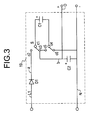
- the preferred embodiment of the present invention is shown in Figure 4 .
- the preferred embodiment replicates and automates the switching function of the mechanical switch S by adding to the circuit a second and third blocking diode D2 , D3 and a high speed, high current, npn darlington transistor pair formed by a first and second transistor Q2 a , Q2 b .
- a first small signal npn transistor Q1 along with a first current limiting resistor R1 coupled to the base 31 of the transistor Q1 monitors the ac zero crossing by coupling the first resistor R1 and the emitter 33 of the first transistor Q1 across the input terminals L1, N .
- the collector 35 of the first transistor Q1 is coupled to the base 37 of the first darlington transistor Q2 a through a second current limiting resistor R2 .
- the first transistor Q1 is turned-on and sinks current through a third resistor R3 during the positive portion of the input waveform (shown in Figures 6B and 6C ).
- transistor Q1 is turned-off (shown in Figures 6B and 6C ).
- a fourth resistor R4 is coupled between the base 37 of the first darlington transistor Q2 a and the emitter 39 of the second darlington transistor Q2 b .
- a fourth diode D4 is placed in parallel across the fourth resistor R4 .
- a third current limiting resistor R3 is coupled between the common node a formed by both collectors 41, 43 of the darlington transistor pair Q2 a , Q2 b , the cathode of the first blocking diode D1 and the positive terminal of the first capacitor C1 to the base 37 of the first darlington transistor Q2 a .
- the cathode of the second blocking diode D2 is connected to a common node c formed by the negative terminal of the first capacitor C1 and the anode of the third blocking diode D3 .
- the cathode of the third blocking diode D3 is connected to the common node b coupling the speed-up resistor R4 , the emitter 39 of the second darlington transistor Q2 b and the positive terminal of the second capacitor C2 forming the positive output O of the converter 19 .
- Coupled to the common input/output bus N is the emitter 33 of the small signal transistor Q1 , the anode of the second blocking diode D2 and the negative terminal of the second capacitor C2 .
- the preferred embodiment as shown in Figure 4 operates similarly to the simplified charging mode shown in Figure 2 and the simplified discharging mode in Figure 3 .
- the small signal transistor Q1 turns-on and turns-off.
- the cyclical turning on and off of the small signal transistor Q1 controls the darlington transistor pair Q2 a , Q2 b which conversely reconfigures the circuit to allow the first and second capacitors C1, C2 to be charged during the positive portion of the ac waveform by the halfwave rectification of the first blocking diode D1 .
- the first capacitor C1 discharges into the second capacitor C2 thereby providing a continuous filtered dc output 0 to the load R L .
- V peak V C1 + V C2 Equation 3
- V peak 2 Q C ; for each capacitor.
- the first capacitor C1 discharges into the second capacitor C2 and the load R L .
- the dc voltage across the second capacitor C2 will be approximately one half of the peak ac input voltage, V peak as long as the capacitance values of the first capacitor C1 and the second capacitor C2 are equal.
- the capacitance of the first capacitor C1 may be slightly less than or equal to the capacitance of the second capacitor C2 so the voltage experienced during initial energization does not exceed V peak /2. If the capacitance of the first capacitor C1 is greater than the capacitance of the second capacitor C2 , the initial energization transient may produce a voltage greater than V peak /2 across the second capacitor depending upon the load R L . After the present invention 19 has been in operation for several cycles, the voltage stabilizes at V peak /2.
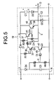
- FIG. 5 An alternative embodiment for the present invention 19 is shown in Figure 5 .
- a voltage monitoring circuit is added to the above described circuit.
- the voltage monitoring circuit includes a fifth diode D5 coupled in series with a third capacitor C3 .
- the series combination is coupled across the line and neutral inputs L1, N with the anode of the fifth diode D5 coupled to the line L1 input.
- a voltage divider having a fifth resistor R5 coupled in series with a sixth resistor R6 is connected in parallel across the third capacitor C3 to create a calculated voltage drop depending on the input voltage.
- the cathode of a regulating fifth Zener diode D5 is coupled to the common node d formed between the fifth and sixth resistors R5, R6 and having the anode coupled to the base 45 of a third npn transistor Q3 .
- the value of the Zener diode D6 is 10V.
- Other Zener values will function with the proper fifth to sixth resistor R5, R6 ratio.
- the collector 47 of the third transistor Q3 interrupts the emitter 33 of the first transistor Q1 .
- the emitter 49 of the third transistor is coupled to the circuit common N .
- the dc voltage across the third capacitor C3 will be approximately 184Vdc or less.
- the voltage divider formed by the fifth and sixth resistors R5, R6 drops approximately 10Vdc across the sixth resistor R6 producing approximately 174Vdc across the fifth resistor R5 .
- the third transistor Q3 will remain off if the input voltage supply 27 is 130V RMS or less thereby preventing the first transistor Q1 from turning-on which keeps the darlington pair Q2 a , Q2 b fully on maintaining the circuit as a halfwave rectifier. For input voltages greater than 130V RMS , the third transistor Q3 turns-on and permits the circuit to operate as described earlier.
Landscapes
- Engineering & Computer Science (AREA)
- Power Engineering (AREA)
- Rectifiers (AREA)
- Dc-Dc Converters (AREA)
- Ac-Ac Conversion (AREA)
Applications Claiming Priority (2)
| Application Number | Priority Date | Filing Date | Title |
|---|---|---|---|
| US08/929,714 US5914869A (en) | 1997-09-15 | 1997-09-15 | Ac/dc transformerless voltage converter |
| US929714 | 1997-09-15 |
Publications (2)
| Publication Number | Publication Date |
|---|---|
| EP0902530A2 true EP0902530A2 (de) | 1999-03-17 |
| EP0902530A3 EP0902530A3 (de) | 2000-05-10 |
Family
ID=25458332
Family Applications (1)
| Application Number | Title | Priority Date | Filing Date |
|---|---|---|---|
| EP98304540A Withdrawn EP0902530A3 (de) | 1997-09-15 | 1998-06-09 | Spannungswandler |
Country Status (5)
| Country | Link |
|---|---|
| US (1) | US5914869A (de) |
| EP (1) | EP0902530A3 (de) |
| JP (1) | JPH11252921A (de) |
| AU (1) | AU7991998A (de) |
| CA (1) | CA2237288A1 (de) |
Families Citing this family (10)
| Publication number | Priority date | Publication date | Assignee | Title |
|---|---|---|---|---|
| JP3475138B2 (ja) * | 1999-12-08 | 2003-12-08 | 三洋電機株式会社 | チャージポンプ回路 |
| JP3475173B2 (ja) * | 1999-12-08 | 2003-12-08 | 三洋電機株式会社 | チャージポンプ回路 |
| US6583522B1 (en) * | 2000-09-27 | 2003-06-24 | Worldwater Corp. | Switchable multiple source power supply |
| US6597591B2 (en) * | 2001-12-03 | 2003-07-22 | Adda Corporation | Transformerless AC/DC converter |
| US7737658B2 (en) * | 2003-10-27 | 2010-06-15 | Sony Corporation | Battery packs having a charging mode and a discharging mode |
| JP2005284710A (ja) | 2004-03-30 | 2005-10-13 | Sanyo Electric Co Ltd | 駆動回路 |
| TWI344258B (en) * | 2005-08-19 | 2011-06-21 | Delta Electronics Inc | Motor driving method and device thereof |
| US8233301B1 (en) | 2008-12-20 | 2012-07-31 | Sensorlink Corporation | Impedance dropping dc power supply having an impedance controlled converter |
| CN102244955B (zh) * | 2010-05-14 | 2015-12-30 | 皇家飞利浦电子股份有限公司 | 自适应电路 |
| US10389507B2 (en) * | 2015-10-20 | 2019-08-20 | Analog Devices Global | System for power transfer and duplex communication via single isolation device |
Family Cites Families (6)
| Publication number | Priority date | Publication date | Assignee | Title |
|---|---|---|---|---|
| US3213350A (en) * | 1961-07-03 | 1965-10-19 | Charles J Armour | Voltage regulator means interrupting load current upon excessive load voltages |
| JPS6025391U (ja) * | 1983-07-27 | 1985-02-21 | 日本ケミコン株式会社 | 電源装置 |
| AT384694B (de) * | 1985-12-10 | 1987-12-28 | Uher Ag | Spannungswandlerschalter |
| US4882665A (en) * | 1988-06-10 | 1989-11-21 | Choi Keh Kun | High frequency, high power, power supply |
| JPH02146955A (ja) * | 1988-08-30 | 1990-06-06 | Michiko Naito | 静電トランス |
| EP0560666A2 (de) * | 1992-03-10 | 1993-09-15 | Fu Ming Zhou | Gleichspannungsteiler |
-
1997
- 1997-09-15 US US08/929,714 patent/US5914869A/en not_active Expired - Lifetime
-
1998
- 1998-05-11 CA CA002237288A patent/CA2237288A1/en not_active Abandoned
- 1998-06-09 EP EP98304540A patent/EP0902530A3/de not_active Withdrawn
- 1998-07-24 JP JP10210033A patent/JPH11252921A/ja active Pending
- 1998-08-11 AU AU79919/98A patent/AU7991998A/en not_active Abandoned
Also Published As
| Publication number | Publication date |
|---|---|
| JPH11252921A (ja) | 1999-09-17 |
| US5914869A (en) | 1999-06-22 |
| CA2237288A1 (en) | 1999-03-15 |
| AU7991998A (en) | 1999-03-25 |
| EP0902530A3 (de) | 2000-05-10 |
Similar Documents
| Publication | Publication Date | Title |
|---|---|---|
| US6154380A (en) | AC/DC boost converter | |
| KR100378801B1 (ko) | 직류 전원 회로 | |
| US5638262A (en) | Method and apparatus for providing isolated power sourced from bleeder current | |
| US5144544A (en) | Power feed system for telephone and/or information technology terminals | |
| CN110995025A (zh) | 一种开关电源电路 | |
| TWI590574B (zh) | 電源供應裝置 | |
| CA2521211C (en) | Switching power supply with capacitor input for a wide range of ac input voltages | |
| US4736286A (en) | Switching power supply | |
| AU696737B2 (en) | High efficiency voltage converter and regulator circuit | |
| US5914869A (en) | Ac/dc transformerless voltage converter | |
| US4219872A (en) | Power supply | |
| US5798630A (en) | Switching power circuit to supply electric-vehicle battery charger with high-frequency power | |
| US6462924B1 (en) | Power supply apparatus comprising a voltage detection circuit and method for using same | |
| US6909617B1 (en) | Zero-voltage-switched, full-bridge, phase-shifted DC-DC converter with improved light/no-load operation | |
| EP0090782A2 (de) | Gleichstrom-Gleichstrom-Sperrwandler mit niedriger Welligkeit im Ausgangskondensator | |
| US6072709A (en) | Multiple output voltage converter with improved cross-regulation | |
| CN113726175B (zh) | 转换装置、控制器及其供电控制方法 | |
| GB2206982A (en) | Direct current power supply | |
| HK66996A (en) | Circuit arrangement for powering a load | |
| CN109286321A (zh) | 开关电源电路 | |
| US11916492B2 (en) | Device for supplying power from an AC voltage | |
| US10917088B1 (en) | Power conversion device | |
| US20220115956A1 (en) | Flyback converter and electronic device | |
| CN211046770U (zh) | 一种电源电路及电子设备 | |
| CN216362285U (zh) | 一种电源电路与电子设备 |
Legal Events
| Date | Code | Title | Description |
|---|---|---|---|
| PUAI | Public reference made under article 153(3) epc to a published international application that has entered the european phase |
Free format text: ORIGINAL CODE: 0009012 |
|
| AK | Designated contracting states |
Kind code of ref document: A2 Designated state(s): AT BE CH CY DE DK LI |
|
| AX | Request for extension of the european patent |
Free format text: AL;LT;LV;MK;RO;SI |
|
| PUAL | Search report despatched |
Free format text: ORIGINAL CODE: 0009013 |
|
| AK | Designated contracting states |
Kind code of ref document: A3 Designated state(s): AT BE CH CY DE DK ES FI FR GB GR IE IT LI LU MC NL PT SE |
|
| AX | Request for extension of the european patent |
Free format text: AL;LT;LV;MK;RO;SI |
|
| 17P | Request for examination filed |
Effective date: 20001106 |
|
| AKX | Designation fees paid |
Free format text: AT BE CH CY DE DK LI |
|
| RBV | Designated contracting states (corrected) |
Designated state(s): DE ES FR GB IE IT |
|
| 17Q | First examination report despatched |
Effective date: 20010228 |
|
| STAA | Information on the status of an ep patent application or granted ep patent |
Free format text: STATUS: THE APPLICATION IS DEEMED TO BE WITHDRAWN |
|
| 18D | Application deemed to be withdrawn |
Effective date: 20010911 |