EP0902924B1 - Circuit memoire redondant avec cellules de memoire rom - Google Patents
Circuit memoire redondant avec cellules de memoire rom Download PDFInfo
- Publication number
- EP0902924B1 EP0902924B1 EP97930292A EP97930292A EP0902924B1 EP 0902924 B1 EP0902924 B1 EP 0902924B1 EP 97930292 A EP97930292 A EP 97930292A EP 97930292 A EP97930292 A EP 97930292A EP 0902924 B1 EP0902924 B1 EP 0902924B1
- Authority
- EP
- European Patent Office
- Prior art keywords
- memory cells
- redundancy
- data
- units
- unit
- Prior art date
- Legal status (The legal status is an assumption and is not a legal conclusion. Google has not performed a legal analysis and makes no representation as to the accuracy of the status listed.)
- Expired - Lifetime
Links
- 230000015654 memory Effects 0.000 title claims abstract description 239
- 210000000352 storage cell Anatomy 0.000 title description 2
- 230000008439 repair process Effects 0.000 claims description 20
- 238000001514 detection method Methods 0.000 claims description 17
- 239000003990 capacitor Substances 0.000 claims description 12
- 238000012937 correction Methods 0.000 claims description 9
- 230000004913 activation Effects 0.000 claims description 7
- 230000008901 benefit Effects 0.000 abstract description 3
- 210000004027 cell Anatomy 0.000 description 166
- 238000004519 manufacturing process Methods 0.000 description 13
- 238000012360 testing method Methods 0.000 description 6
- 230000002950 deficient Effects 0.000 description 4
- 230000007547 defect Effects 0.000 description 3
- 230000006870 function Effects 0.000 description 2
- FFBHFFJDDLITSX-UHFFFAOYSA-N benzyl N-[2-hydroxy-4-(3-oxomorpholin-4-yl)phenyl]carbamate Chemical compound OC1=C(NC(=O)OCC2=CC=CC=C2)C=CC(=C1)N1CCOCC1=O FFBHFFJDDLITSX-UHFFFAOYSA-N 0.000 description 1
- 230000009849 deactivation Effects 0.000 description 1
- 238000011161 development Methods 0.000 description 1
- 230000018109 developmental process Effects 0.000 description 1
- 238000000638 solvent extraction Methods 0.000 description 1
- 238000012549 training Methods 0.000 description 1
Images


Classifications
-
- G—PHYSICS
- G11—INFORMATION STORAGE
- G11C—STATIC STORES
- G11C29/00—Checking stores for correct operation ; Subsequent repair; Testing stores during standby or offline operation
- G11C29/70—Masking faults in memories by using spares or by reconfiguring
- G11C29/72—Masking faults in memories by using spares or by reconfiguring with optimized replacement algorithms
-
- G—PHYSICS
- G11—INFORMATION STORAGE
- G11C—STATIC STORES
- G11C11/00—Digital stores characterised by the use of particular electric or magnetic storage elements; Storage elements therefor
- G11C11/005—Digital stores characterised by the use of particular electric or magnetic storage elements; Storage elements therefor comprising combined but independently operative RAM-ROM, RAM-PROM, RAM-EPROM cells
-
- G—PHYSICS
- G11—INFORMATION STORAGE
- G11C—STATIC STORES
- G11C29/00—Checking stores for correct operation ; Subsequent repair; Testing stores during standby or offline operation
- G11C29/04—Detection or location of defective memory elements, e.g. cell constructio details, timing of test signals
- G11C29/08—Functional testing, e.g. testing during refresh, power-on self testing [POST] or distributed testing
- G11C29/12—Built-in arrangements for testing, e.g. built-in self testing [BIST] or interconnection details
- G11C29/18—Address generation devices; Devices for accessing memories, e.g. details of addressing circuits
- G11C29/24—Accessing extra cells, e.g. dummy cells or redundant cells
-
- G—PHYSICS
- G11—INFORMATION STORAGE
- G11C—STATIC STORES
- G11C29/00—Checking stores for correct operation ; Subsequent repair; Testing stores during standby or offline operation
- G11C29/70—Masking faults in memories by using spares or by reconfiguring
- G11C29/78—Masking faults in memories by using spares or by reconfiguring using programmable devices
Definitions
- the invention relates to a redundancy concept for integrated Memory circuits with ROM memory cells.
- RAM memories random access memory, read and write memory
- redundant word or bit lines are also RAM memory cells like that Have "normal” word and bit lines.
- a repairable ROM memory is described in US Pat. No. 4,601,031, where a broken row of ROM memory cells replaced by a redundant row with RAM memory cells becomes. Each column of the ROM memory cell array contains one Check bit and the data to be stored in the redundant row are reconstructed using this check bit. In the Initialization of the memory will be reconstructed data in written the redundant row.
- the invention has for its object a memory circuit specify with ROM memory cells in which the redundant Storage cells have a small footprint.
- "normal" addressable is provided first units with ROM memory cells through redundant to replace addressable second units with RAM memory cells.
- the first and second units can e.g. Word or bit lines or possibly even entire memory blocks his.
- a memory test is preferably carried out immediately after the manufacturing process of the memory. Then that's it Defective replacement of the first units according to the invention can be undertaken.
- the memory cell contents of the replaced ROM memory cells in the volatile redundant RAM memory cells restoring sees a training the invention before each start of the memory (i.e. when applying the supply voltage) an initialization perform, in which these memory cell contents are reconstructed and stored in the RAM memory cells.
- This initialization of the memory is by means of a processor feasible.
- redundant RAM memory cells has the advantage on that these can be realized on a smaller area than PROM memory cells that act as redundant memory cells of the above-mentioned US-A 5,388,076. This especially applies when it comes to redundant DRAM memory cells (Dynamic RAM) is acting.
- DROM memories Dynamic ROM
- DROMs are a variant of a ROM and have ROM memory cells that have the same structure and the same Have cell structure like DRAM memory cells. These ROM memory cells have the same electrical components and the same dimensions as RAM memory cells.
- a DROM is easily done by slightly changing the Manufacturing process of a DRAM can be produced and achieved such a ROM with memory cells that are just as small as DRAM memory cells are.
- At least some of the ROM memory cells of a DROM are included compared to normal DRAM memory cells in their structure modified: For example, in a first implementation the electrical connection between a selection transistor and a memory cell capacitor of the DRAM memory cell be present in a ROM memory cell, if a date of a first logic state in the ROM memory cell is saved. To save a date a second logical state, however, is not an electrical one Connection between selection transistor and memory cell capacitor the corresponding ROM memory cell. In the memory cell capacitor of the latter, modified Memory cells cannot store any charge be so that when reading the memory cell via the selection transistor the potential of one with the selection transistor connected bit line remains almost unaffected.
- a second form of implementation for the ROM memory cells DROMs provides the one normally associated with the memory cell capacitor connected connection of the selection transistor to connect with different fixed potentials, depending on the logical state of the data to be saved (this is shown in the above-mentioned US-A 5,388,076).
- Figure 1 shows schematically an integrated according to the invention Storage.
- This has bit lines BL, "normal" word lines WL and redundant word lines WL ', in their crossing points Memory cells 11, 12, 13 are arranged.
- a Addressing of the word lines WL is via a word line decoder 20 and addressing the redundant word lines WL via a redundant word line decoder 20 (both are shown as one unit in FIG. 1), while addressing the bit lines BL over a bit line decoder 21 takes place.
- There are word addresses for this WADR or bit addresses BADR to the corresponding decoder 20, 20 ', 21 can be applied.
- the three of the normal word lines WL shown are each individually addressable "normal" first units E1 with ROM memory cells 11.
- the first units E1 are used for operation of the memory if there is no redundancy.
- the redundant word lines WL are redundant second units E2 with RAM memory cells 12 and serve in the event of redundancy an address-based replacement of one of the first units E1.
- one of the normal word lines WL is a third one addressable unit E3 with fixed value memory cells 13.
- a redundancy repair is preferably carried out immediately after the Manufacture of the integrated memory and after implementation a memory test. A broken one of the first Units E1 is then addressable by the second unit E2 replaceable. For this purpose, the redundant word line decoder 20 'to program accordingly, what a conventional Hardware redundancy repair corresponds and therefore that Known expert.
- E3 Parity bits can be stored, which are used to reconstruct the data content of defective ROM memory cells 11 by means of Error correction codes in an extended initialization phase serve the store when it is commissioned, as will be explained below.
- This invention Initialization is every time the memory is started up to make because RAM memory cells are known to be volatile Memory are.
- the memory according to the invention in FIG. 1 also shows Redundancy detection means 4 and a repair means 5.
- the redundancy detection means 4 are in the redundancy case the addresses of replaced first units E1 can be determined. Thereupon is a reconstruction through the repair means 5 or repair of those originally replaced in the of the ROM memory cells 11 in the manner to be stored feasible that this data subsequently in the replacing RAM memory cells 12 are stored.
- the second unit E2 is every time the memory is started up an initialization feasible in which the content of volatile, redundant RAM memory cells 12 restored becomes.
- the redundancy detection means 4 and the repair means 5 can be implemented, for example, by a microprocessor be the address recognition of faulty first units and the reconstruction of the incorrect data in the redundant RAM memory cells 12 performs.
- This processor can on the same integrated circuit as the integrated one Storage can be arranged or on a separate integrated Circuit.
- the error correction by the repair means 5 is, for example using error correction codes with the help the parity bits stored in the third units E3 feasible.
- the parity bits allow reconstruction single memory error within one of the word lines WL with the help of the others, in the memory cells of this Word line WL stored data.
- the third units E3 with the fixed value memory cells 13 in the same memory cell array as that to arrange first units E1. Then the fixed value memory cells 13 of the same type of memory cell as that ROM memory cells 11 (e.g. DROM memory cells). But it is alternatively also possible that the third units E3 in one arranged separately from the first units E1 are.
- a third unit E3 instead of individual parity bits (a third unit E3) also parity symbols with several parity bits, e.g. Parity bytes be provided. Then there are several third units E3 available.
- Error correction codes for the reconstruction of incorrectly stored Data are known to those skilled in the art and are here not explained further. Only the Reed-Solomon code is an example and called the Hamming code.
- Figure 1 shows an example of only a few normal word lines WL and a redundant word line WL 'and a few bit lines BL.
- real memory has a lot more such lines on.
- the invention is alternatively or additionally instead of on word line redundancy of course also applicable to bit line redundancy.
- FIG. 2 shows a possible embodiment as a detailed view some of the ROM memory cells 11 and the RAM memory cells 12 from Figure 1.
- the bit lines BL and one of the word lines WL first unit E1
- only one of the redundant word lines WL ' second unit E2
- the integrated Memory is a DROM memory.
- the section of the integrated memory shown includes two "normal” or “regular” ROM memory cells 11 and two redundant RAM memory cells 12, the one-transistor DRAM memory cells are.
- DROMs have ROM memory cells that have the same cell structure like DRAM memory cells.
- Each of the ROM memory cells 11 and the RAM memory cells 12 therefore points a selection transistor T and a memory cell capacitor C on.
- the ROM memory cell 11 at the top left in FIG. 2 has one electrical connection between the selection transistor T and the memory cell capacitor C, as is the case with the RAM memory cells 12 is the case. In contrast, the ROM memory cell 11 this connection does not exist at the bottom left, it is a modified memory cell 14. The presence or the absence of this electrical connection is during the manufacture of the integrated memory fixed while the ROM memory cells 11 - e.g. by Mask programming - programmed, d. H. described with data become.
- the ROM memory cell 11 is assumed to have been at the top left a date of a first logical state 1 stored while the ROM memory cell 11 bottom left (the modified memory cell 14) a date of a second logic state 0 has been saved. The first one logical state by a high potential and the second logical State defined by a low potential.
- the "normal" word line WL which is the first unit E1 forms, defective as a whole or has individual defects ROM memory cells 11 on (which by a test, for example at the end of the integrated manufacturing process Circuit, but may also be feasible later, can be determined), it is redundant due to the redundant Word line WL '(second unit E2) can be replaced in terms of address.
- This second unit E2 only has RAM memory cells 12 on. It is in the illustrated embodiment RAM memory cells 12 are DRAM memory cells.
- the ROM memory cells 11 for storing data of the first logical state 1 are thus structured exactly like that RAM memory cells 12.
- the initialization according to the invention advantageously takes place use of the redundancy detection means 4 and the repair agent 5.
- the redundancy detection means 4 can be determined whether one and if necessary which first unit E1 by one of the redundant second Units E2 has been replaced. Then are through Repair means 5 in the replacing second units E2 data the correct logical state can be saved as it actually is in the ROM memory cells 11 of the replaced ones first unit E1 should be stored. After graduation this, compared to the initialization practiced so far The initialization phase of an extended DROM is the integrated one Memory ready.
- both the "normal" ROM memory cells 11 and the redundant RAM memory cells 12 also have the same cell structure have a very simple manufacturing process for the integrated memory.
- the area for Realization of the redundant second units E2 is very low, since in particular in this embodiment 1-transistor DRAM memory cells shown a very small Have space requirements.
- the invention is therefore suitable very good for use in DROMs, the manufacture of which is known by modifying a DRAM manufacturing process.
- the invention is not limited to DROMs.
- the redundant RAM memory cells 12 do not necessarily have to 1-transistor DRAM memory cells. Others are coming too RAM memory cells into consideration.
- the fixed value memory cells 13 of the third units E3 can also advantageously DROM memory cells like the ROM memory cells 11 in Figure 2 be. In particular, they can be part of the same Memory cell array like this.
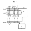
- FIG. 3 shows others in a simplified form of representation Details from the memory of Figure 1.
- the entered logical states 0, 1 should be in the selected Not the actual memory cell content but the desired memory cell content Show correctness of the corresponding first unit E1.
- the desired memory cell content can differ from the actual one Memory cell content due to manufacturing errors the integrated circuit or programming of the ROMS.
- the second unit E2 is redundant RAM memory cells 12 shown to replace one of the first Units El serves in the event of redundancy.
- the third unit E3 has the fixed value memory cells 13 for storing the parity bits P on.
- the first E1, second E2 and third E3 Units are each word lines WL, WL '.
- the redundancy detection means 4 in FIG. 3 contains a fixed value storage means 15, which has as many storage spaces has how first units E1 are present. Through the dashed connecting lines indicate that everyone Storage space of the fixed value storage means 15 advantageously Can be part of one of the first units E1.
- information is stored, which indicate whether the associated first unit E1 is free of errors stored data has modified memory cells 14 or not. As mentioned above, it can happen in a row of manufacturing defects that actually occur instead of one modified memory cell 14 to be manufactured is an unmodified one Memory cell 11 is generated.
- the information in the fixed value storage means 15 are there simultaneously with the Programming the memory can be saved, i.e. usually in the manufacture of the store.
- the fixed value storage means 15 entered a 0 if the associated one first unit E1 in the case of a fault, a modified memory cell 14 has. There is one in the fixed value storage means 15 1 saved when the associated first unit E1 is error-free has no modified memory cells 14.
- Each of the memory cells 11, 12 is filled with data of the first logical State 1 described by the respective first Unit E1 (or in the case of redundancy, the second unit E2 instead of the first unit E1) to be replaced becomes. If the first unit E1 is one, the exclusively unmodified memory cells 11 has, this is based on the redundancy detection means 4 the corresponding entry in the associated fixed value storage means 15 recognizable. For such a first unit E1 with unmodified ROM memory cells 11, which are do not differ in any way from a DRAM memory cell 12 according to FIG. 2, is a replacement in the event of redundancy by the second unit E2 with RAM memory cells 12 completely unproblematic. The second unit E2 then points to that in the Commissioning of the memory performed initialization the data of the first logical state written in the process 1 on. The reconstruction is redundant in these RAM memory cells 12 data already completed.
- the redundancy detection means 4 is based on the corresponding entries in the fixed value storage means 15 notes that it is the first unit addressed E1 is one that is actually modified According to the invention, memory cells 14 should contain after initializing the entire memory with Data of the first logical state 1 at least all memory cells of these first units 1 with modified memory cells 14 read out again. It turns out that a of the first units E1 based on the entry in the fixed value storage means 15 actually modified memory cells 14 should have, when reading the corresponding Address addressed memory cells but only data from the first logical state 1 are read, it is clear that in this case a first one at the corresponding address Unit E1 with modified memory cells 14 by the second unit E2 with RAM memory cells 12 has been replaced is (redundancy case).
- Figure 4 shows another embodiment of details of the Memory in Figure 1.
- the first E1 and second units E2 are, as in Figure 1, "normal" word lines WL or redundant Word lines WL '.
- Word addresses WADR for addressing of the normal word lines WL are through the normal word line decoder 20 decodable and the corresponding word line WL can be selected in this way.
- the word address WADR through a redundancy word line decoder 20 (shown in FIG 1 together with the word line decoder 20 as a unit is shown) decodable. Is a redundancy of the first units E1 replaced by the second unit E2 the corresponding word address WADR is in the redundancy word line decoder 20 'programmed.
- redundancy word line decoder 20 This usually happens by means of separable connections (fuses) in the connection to the manufacture and test of the store. Now the redundancy word line decoder 20 'speaks to an applied one Word address WADR on, it generates a redundancy activation signal REN, which on the one hand leads to a deactivation of the normal word line decoder 20 leads and the other for a selection of the corresponding redundant word line WL '.
- the redundancy activation signal is now provided REN to use by means of the redundancy detection means 4 the addresses of replaced first units E1 to determine. This is due to the redundancy detection means 4 can be registered at which created word addresses WADR the redundancy activation signal REN for selection the second unit E2 by the redundancy word line decoder 20 'is generated. In this way you can find the one you are looking for Determine addresses particularly easily, then follow through the repair means 5 the reconstruction of the data stored in the memory cells to be replaced and storing this data in the memory cells of the second Unit E2 is feasible.
- FIG. 4 shows a register L, in which the redundancy activation signal, if required REN can be saved. This may be necessary be when the processor performing the functions of the redundancy detection means 4 and the repair agent 5, is not capable of multitasking, so that temporary storage in register L before evaluating the redundancy activation signal REN by the redundancy detection means 4 he follows.
- each of these groups having a third unit E3 is assigned to fixed value memory cells 13.
- the invention is not limited to the replacement of ROM memory cells of a DROM is limited by DRAM memory cells. According to the invention there is generally redundancy of any ROM memory cells by any RAM memory cells possible.
- DROM which has two types of ROM memory cells (namely modified and unmodified memory cells), for both types of memory cells RAM memory cells as To provide redundancy.
- the invention is also applicable to memories that have both DROM and DRAM areas exhibit.
Landscapes
- Engineering & Computer Science (AREA)
- Computer Hardware Design (AREA)
- For Increasing The Reliability Of Semiconductor Memories (AREA)
- Techniques For Improving Reliability Of Storages (AREA)
Claims (5)
- Circuit mémoireavec des premières unités (E1), qui peuvent être adressées individuellement, avec des cellules de mémoire ROM (11) et avec au moins une deuxième unité redondante (E2) avec des cellules de mémoire RAM (12), qui sert, en cas de redondance, au remplacement du point de vue de l'adressage de l'une des premières unités (E1),avec un moyen (4) de détection de la redondance pour la détermination de l'adresse de la première unité (E1) remplacée, en cas de redondance, par la deuxième unité (E2),avec un moyen (5) de réparation pour déterminer, immédiatement après, des données, destinées à l'origine à être stockées dans les cellules de mémoire ROM (11) remplacées, et pour stocker ces données dans les cellules de mémoire RAM (12) qui les remplacent,dans lequel les cellules de mémoire RAM (12) comportent un transistor (T) de sélection et un condensateur (C) de mémorisation, qui lui est raccordé électriquement,dans lequel celles des cellules de mémoire ROM (11), qui sont destinées à stocker des données d'un premier état logique (1), sont conçues de la même façon que les cellules de mémoire RAM (12) etdans lequel celles des cellules de mémoire ROM (11), qui sont destinées à stocker des données d'un deuxième état logique (0), sont des cellules de mémoire modifiées (14) qui se distinguent des cellules de mémoire RAM (12) par le fait que, dans celles-ci, la liaison électrique entre le transistor (T) de sélection et le condensateur (C) de mémorisation est interrompue.
- Circuit mémoire selon la revendication 1,qui comporte une troisième unité adressable (E3) avec des cellules de mémoire à valeur fixe (E3), dans lesquelles sont stockés des bits de parité (P) etdans lequel la détermination des données destinées à l'origine à être stockées dans les cellules de mémoire ROM (11) remplacées est effectuée par le moyen (5) de réparation à l'aide de codes de correction d'erreurs en faisant appel à des bits de parité (P).
- Circuit mémoire selon la revendication 1 ou 2dans lequel, pour déterminer si une des premières unités (E1) avec des cellules de mémoire modifiées (14) a été remplacée, en cas de redondance, par la deuxième unité (E2), des données du premier état logique (1) sont écrites dans toutes les cellules de mémoire (11, 12), puis relues sur ces cellules de mémoire (11, 12), qui sont adressées par application de l'adresse (WADR) de cette première unité (E1) avec des cellules de mémoire modifiées (14), etdans lequel, immédiatement après, une comparaison est effectuée entre les données écrites et les données relues,la détermination des données destinées à l'origine à être stockées et le stockage de ces données dans les cellules de mémoire correspondant à l'adresse (WADR) respective n'ayant lieu que si les données écrites et les données relues concordent.
- Circuit mémoire selon la revendication 3
dans lequel le moyen (4) de détection de la redondance comporte un moyen de mémorisation à valeur fixe (15), dans lequel sont mémorisées, celles des premières unités (E1) qui, en cas d'absence d'erreur, contiennent des cellules de mémoire modifiées (14). - Circuit mémoire selon l'une des revendications précédentes
dans lequel, pour la détermination de l'adresse des unités remplacées parmi les premières unités (E1), est appliqué, sur le moyen (4) de détection de la redondance, un signal (REN) d'activation de la redondance, généré par un décodeur de redondance (20') et servant à activer la deuxième unité (E2).
Applications Claiming Priority (3)
| Application Number | Priority Date | Filing Date | Title |
|---|---|---|---|
| DE19622275A DE19622275A1 (de) | 1996-06-03 | 1996-06-03 | Redundanzkonzept für integrierte Speicher mit ROM-Speicherzellen |
| DE19622275 | 1996-06-03 | ||
| PCT/DE1997/001016 WO1997046942A1 (fr) | 1996-06-03 | 1997-05-21 | Conception de la redondance pour circuits de memoire avec cellules de memoire rom |
Publications (2)
| Publication Number | Publication Date |
|---|---|
| EP0902924A1 EP0902924A1 (fr) | 1999-03-24 |
| EP0902924B1 true EP0902924B1 (fr) | 2001-04-04 |
Family
ID=7796036
Family Applications (1)
| Application Number | Title | Priority Date | Filing Date |
|---|---|---|---|
| EP97930292A Expired - Lifetime EP0902924B1 (fr) | 1996-06-03 | 1997-05-21 | Circuit memoire redondant avec cellules de memoire rom |
Country Status (5)
| Country | Link |
|---|---|
| US (1) | US5986952A (fr) |
| EP (1) | EP0902924B1 (fr) |
| DE (2) | DE19622275A1 (fr) |
| TW (1) | TW371759B (fr) |
| WO (1) | WO1997046942A1 (fr) |
Families Citing this family (11)
| Publication number | Priority date | Publication date | Assignee | Title |
|---|---|---|---|---|
| JP2000298997A (ja) * | 1999-04-15 | 2000-10-24 | Nec Corp | 半導体メモリ装置、データ設定方法および装置、情報記憶媒体 |
| US7069482B1 (en) * | 2000-08-21 | 2006-06-27 | Nanoamp Solutions, Inc. | ROM error-correction control |
| US6421283B1 (en) * | 2000-09-27 | 2002-07-16 | Conexant Systems, Inc. | Trap and patch system for virtual replacement of defective volatile memory cells |
| US6545899B1 (en) * | 2001-12-12 | 2003-04-08 | Micron Technology, Inc. | ROM embedded DRAM with bias sensing |
| US20030115538A1 (en) * | 2001-12-13 | 2003-06-19 | Micron Technology, Inc. | Error correction in ROM embedded DRAM |
| US20030185062A1 (en) * | 2002-03-28 | 2003-10-02 | Micron Technology, Inc. | Proximity lookup for large arrays |
| US7174477B2 (en) * | 2003-02-04 | 2007-02-06 | Micron Technology, Inc. | ROM redundancy in ROM embedded DRAM |
| JP3935151B2 (ja) * | 2004-01-26 | 2007-06-20 | 株式会社東芝 | 半導体集積回路装置 |
| US8381019B2 (en) * | 2010-06-24 | 2013-02-19 | International Business Machines Corporation | EDRAM macro disablement in cache memory |
| KR102492033B1 (ko) * | 2018-03-26 | 2023-01-26 | 에스케이하이닉스 주식회사 | 메모리 장치 및 이를 포함하는 메모리 시스템 |
| CN109831815B (zh) * | 2018-12-14 | 2021-10-08 | 中磊电子股份有限公司 | 数据传输协调系统及其方法 |
Family Cites Families (6)
| Publication number | Priority date | Publication date | Assignee | Title |
|---|---|---|---|---|
| GB2129585B (en) * | 1982-10-29 | 1986-03-05 | Inmos Ltd | Memory system including a faulty rom array |
| KR900006155B1 (ko) * | 1985-09-04 | 1990-08-24 | 후지쓰 가부시끼가이샤 | 프로그래머블 반도체 리드 온리 메모리 장치 |
| JPH0683716A (ja) * | 1992-09-01 | 1994-03-25 | Rohm Co Ltd | 電気的書換可能型不揮発メモリ |
| JP3265076B2 (ja) * | 1993-09-20 | 2002-03-11 | 株式会社東芝 | 半導体記憶装置 |
| KR0140178B1 (ko) * | 1994-12-29 | 1998-07-15 | 김광호 | 반도체 메모리장치의 결함 셀 구제회로 및 방법 |
| US5644541A (en) * | 1995-11-03 | 1997-07-01 | Philip K. Siu | Memory substitution system and method for correcting partially defective memories |
-
1996
- 1996-06-03 DE DE19622275A patent/DE19622275A1/de not_active Withdrawn
-
1997
- 1997-05-21 DE DE59703299T patent/DE59703299D1/de not_active Expired - Fee Related
- 1997-05-21 WO PCT/DE1997/001016 patent/WO1997046942A1/fr not_active Ceased
- 1997-05-21 EP EP97930292A patent/EP0902924B1/fr not_active Expired - Lifetime
- 1997-05-27 TW TW086107165A patent/TW371759B/zh active
-
1998
- 1998-12-03 US US09/204,927 patent/US5986952A/en not_active Expired - Lifetime
Also Published As
| Publication number | Publication date |
|---|---|
| WO1997046942A1 (fr) | 1997-12-11 |
| DE59703299D1 (de) | 2001-05-10 |
| US5986952A (en) | 1999-11-16 |
| DE19622275A1 (de) | 1997-12-04 |
| EP0902924A1 (fr) | 1999-03-24 |
| TW371759B (en) | 1999-10-11 |
Similar Documents
| Publication | Publication Date | Title |
|---|---|---|
| DE68928112T2 (de) | Masken-rom mit Ersatzspeicherzellen | |
| DE2328869A1 (de) | Verfahren zur pruefung eines digitalen speichersystems sowie zur durchfuehrung dieses verfahrens dienendes selbstpruefendes digitales speichersystem | |
| EP1008993B1 (fr) | Mémoire avec dispositif de auto-test et sa mèthode | |
| EP0902924B1 (fr) | Circuit memoire redondant avec cellules de memoire rom | |
| EP1113362B1 (fr) | Mémoire de semiconducteur intégrée avec une unité de mémoire pour le stockage des adresses de cellules de mémoire défectueuses | |
| EP1124232A2 (fr) | Mémoire de semiconducteur intégrée avec l'unité redondante des cellules de mémoire | |
| DE10206689B4 (de) | Integrierter Speicher und Verfahren zum Betrieb eines integrierten Speichers | |
| WO2000013087A1 (fr) | Procede de reparation de cellules defectueuses d'une memoire integree | |
| DE102020134945A1 (de) | Dynamische fehlerüberwachung und -reparatur | |
| DE69426818T2 (de) | Fehlertolerantes Speichergerät, insbesondere des Typs "flash EEPROM" | |
| DE69032844T2 (de) | Halbleiterspeicher mit Einrichtung zum Ersetzen defekter Speicherzellen | |
| DE69100796T2 (de) | Integrierte Speicherschaltung mit Redundanz und verbesserter Adressierung in Testbetriebsart. | |
| EP0990236B1 (fr) | Dispositif dote de cellules memoire et procede de controle du bon fonctionnement des cellules memoire | |
| EP0615211A1 (fr) | Dispositif pour mémoriser des données de sécurité | |
| EP1102168B1 (fr) | Mémoire intégrée avec des cellules de mémoire et des cellules de référence | |
| DE69300165T2 (de) | Verfahren zur Reparatur defekter Elemente in einem Redundanzspeicher. | |
| EP1085523B1 (fr) | Mémoire integrée avec cellules de mémoire et cellules de référence | |
| DE69509965T2 (de) | Redundante Schmelzsicherungsmatrixanordnung für integrierten Speicher sowie Verfahren zu ihrem Betrieb | |
| DE19924153B4 (de) | Schaltungsanordnung zur Reparatur eines Halbleiterspeichers | |
| DE10311373B4 (de) | Integrierter Speicher mit redundanten Einheiten von Speicherzellen und Verfahren zum Test eines integrierten Speichers | |
| DE10307027A1 (de) | Verfahren und Testeinrichtung zum Ermitteln einer Reparaturlösung für einen Speicherbaustein | |
| EP1163679B1 (fr) | Procede permettant de faire fonctionner une memoire integree a cellules inscriptibles et memoire integree associee | |
| DE60208376T2 (de) | Verfahren zum Speichern von Fehlern einer Speichervorrichtung in einem Diagnosefeld mit minimaler Speicherkapazität | |
| DE4223273C2 (de) | Halbleiterspeichereinrichtung und Betriebsverfahren für eine solche | |
| DE10146931B4 (de) | Verfahren und Anordnung zum Ersetzen fehlerhafter Speicherzellen in Datenverarbeitungsvorrichtungen |
Legal Events
| Date | Code | Title | Description |
|---|---|---|---|
| PUAI | Public reference made under article 153(3) epc to a published international application that has entered the european phase |
Free format text: ORIGINAL CODE: 0009012 |
|
| 17P | Request for examination filed |
Effective date: 19981117 |
|
| AK | Designated contracting states |
Kind code of ref document: A1 Designated state(s): DE FR GB IE IT |
|
| RTI1 | Title (correction) |
Free format text: REDUNDANCY MEMORY CIRCUIT WITH ROM STORAGE CELLS |
|
| GRAG | Despatch of communication of intention to grant |
Free format text: ORIGINAL CODE: EPIDOS AGRA |
|
| GRAG | Despatch of communication of intention to grant |
Free format text: ORIGINAL CODE: EPIDOS AGRA |
|
| GRAH | Despatch of communication of intention to grant a patent |
Free format text: ORIGINAL CODE: EPIDOS IGRA |
|
| 17Q | First examination report despatched |
Effective date: 20000912 |
|
| GRAH | Despatch of communication of intention to grant a patent |
Free format text: ORIGINAL CODE: EPIDOS IGRA |
|
| RAP1 | Party data changed (applicant data changed or rights of an application transferred) |
Owner name: INFINEON TECHNOLOGIES AG |
|
| GRAA | (expected) grant |
Free format text: ORIGINAL CODE: 0009210 |
|
| AK | Designated contracting states |
Kind code of ref document: B1 Designated state(s): DE FR GB IE IT |
|
| REG | Reference to a national code |
Ref country code: IE Ref legal event code: FG4D Free format text: GERMAN |
|
| REF | Corresponds to: |
Ref document number: 59703299 Country of ref document: DE Date of ref document: 20010510 |
|
| ET | Fr: translation filed | ||
| ITF | It: translation for a ep patent filed | ||
| GBT | Gb: translation of ep patent filed (gb section 77(6)(a)/1977) |
Effective date: 20010618 |
|
| REG | Reference to a national code |
Ref country code: GB Ref legal event code: IF02 |
|
| PLBE | No opposition filed within time limit |
Free format text: ORIGINAL CODE: 0009261 |
|
| STAA | Information on the status of an ep patent application or granted ep patent |
Free format text: STATUS: NO OPPOSITION FILED WITHIN TIME LIMIT |
|
| 26N | No opposition filed | ||
| PGFP | Annual fee paid to national office [announced via postgrant information from national office to epo] |
Ref country code: GB Payment date: 20070522 Year of fee payment: 11 |
|
| PGFP | Annual fee paid to national office [announced via postgrant information from national office to epo] |
Ref country code: IT Payment date: 20080524 Year of fee payment: 12 |
|
| PGFP | Annual fee paid to national office [announced via postgrant information from national office to epo] |
Ref country code: IE Payment date: 20080523 Year of fee payment: 12 Ref country code: DE Payment date: 20080715 Year of fee payment: 12 |
|
| GBPC | Gb: european patent ceased through non-payment of renewal fee |
Effective date: 20080521 |
|
| PG25 | Lapsed in a contracting state [announced via postgrant information from national office to epo] |
Ref country code: GB Free format text: LAPSE BECAUSE OF NON-PAYMENT OF DUE FEES Effective date: 20080521 |
|
| REG | Reference to a national code |
Ref country code: FR Ref legal event code: ST Effective date: 20100129 |
|
| REG | Reference to a national code |
Ref country code: IE Ref legal event code: MM4A |
|
| PG25 | Lapsed in a contracting state [announced via postgrant information from national office to epo] |
Ref country code: IE Free format text: LAPSE BECAUSE OF NON-PAYMENT OF DUE FEES Effective date: 20090521 Ref country code: FR Free format text: LAPSE BECAUSE OF NON-PAYMENT OF DUE FEES Effective date: 20090602 |
|
| PGFP | Annual fee paid to national office [announced via postgrant information from national office to epo] |
Ref country code: FR Payment date: 20080526 Year of fee payment: 12 |
|
| PG25 | Lapsed in a contracting state [announced via postgrant information from national office to epo] |
Ref country code: DE Free format text: LAPSE BECAUSE OF NON-PAYMENT OF DUE FEES Effective date: 20091201 |
|
| PG25 | Lapsed in a contracting state [announced via postgrant information from national office to epo] |
Ref country code: IT Free format text: LAPSE BECAUSE OF NON-PAYMENT OF DUE FEES Effective date: 20090521 |