EP0902988B1 - Circuit de commutation multi-acces hf - Google Patents
Circuit de commutation multi-acces hf Download PDFInfo
- Publication number
- EP0902988B1 EP0902988B1 EP98905160A EP98905160A EP0902988B1 EP 0902988 B1 EP0902988 B1 EP 0902988B1 EP 98905160 A EP98905160 A EP 98905160A EP 98905160 A EP98905160 A EP 98905160A EP 0902988 B1 EP0902988 B1 EP 0902988B1
- Authority
- EP
- European Patent Office
- Prior art keywords
- port
- switching
- ports
- state
- switching circuit
- Prior art date
- Legal status (The legal status is an assumption and is not a legal conclusion. Google has not performed a legal analysis and makes no representation as to the accuracy of the status listed.)
- Expired - Lifetime
Links
- 230000005540 biological transmission Effects 0.000 claims description 25
- 238000000034 method Methods 0.000 claims description 15
- 230000008569 process Effects 0.000 claims description 7
- 239000003990 capacitor Substances 0.000 claims description 3
- 230000009471 action Effects 0.000 claims description 2
- 230000004044 response Effects 0.000 description 6
- 238000002955 isolation Methods 0.000 description 4
- 238000006243 chemical reaction Methods 0.000 description 3
- 238000005516 engineering process Methods 0.000 description 2
- 238000004519 manufacturing process Methods 0.000 description 2
- 229910001218 Gallium arsenide Inorganic materials 0.000 description 1
- 230000003321 amplification Effects 0.000 description 1
- 230000008901 benefit Effects 0.000 description 1
- 230000008859 change Effects 0.000 description 1
- 238000007796 conventional method Methods 0.000 description 1
- 230000009977 dual effect Effects 0.000 description 1
- 230000000694 effects Effects 0.000 description 1
- 230000005669 field effect Effects 0.000 description 1
- 238000003199 nucleic acid amplification method Methods 0.000 description 1
- 238000010615 ring circuit Methods 0.000 description 1
- 230000008054 signal transmission Effects 0.000 description 1
- 239000000758 substrate Substances 0.000 description 1
Images


Classifications
-
- H—ELECTRICITY
- H01—ELECTRIC ELEMENTS
- H01P—WAVEGUIDES; RESONATORS, LINES, OR OTHER DEVICES OF THE WAVEGUIDE TYPE
- H01P1/00—Auxiliary devices
- H01P1/10—Auxiliary devices for switching or interrupting
- H01P1/15—Auxiliary devices for switching or interrupting by semiconductor devices
Definitions
- This invention concerns a multi-port switching circuit.
- the embodiments of one realisation may operate at frequencies around 60 GHz; but with appropriate devices embodiments may operate at other frequencies including higher frequencies up to and even exceeding 100 GHz.
- Switching networks have been developed which operate at frequencies up to and exceeding 40 GHz.
- the switching elements in such networks use a combination of shunt passive FET devices and quarter-wave transformers, or combinations of series and shunt passive FET devices.
- Passive FET devices in one type of switch, require bias to be applied to the gate and not between the source and drain. Broadband switches using a combination of active and passive switching elements have also been demonstrated.
- GB-A-2 121 239, US-A-4 151 489 and US-A-4 129 838 show examples of switched ring-circuits.
- the invention provides a multi-port switching circuit, comprising at least three ports, interconnected by transmission lines.
- the transmission lines are arranged with a central ring and outwardly extending arms.
- the ports are positioned at the ends of respective arms.
- ring has been used in a loose descriptive sense and does not necessarily imply circularity.
- a switching device such as a FET or HEMT, is associated with each port.
- the switching device is arranged between a first and a second transmission line.
- Each switching device may be arranged to shunt the main signal path of the circuit with its main current path extending between the junction of the first and the second transmission line, and signal ground.
- the first transmission line extends between the port and the switching device to provide impedance matching, and the second transmission line also provides impedance matching and a connecting path to the ring.
- the first and second transmission lines are initially chosen to have lengths of a quarter wavelength at the centre of the band of operation of the switch. The dimensions of the matching lines and the lines which form the connections to the ring are then determined using a procedure to optimise the performance of the circuit.
- the optimisation procedure involves the selection of two of the ports as the input and output ports of the switching network.
- the switching devices associated with these ports are modelled by ON state representations.
- the other port, or ports, are isolated, and their associated switching devices are modelled in the OFF state.
- Optimisation of the transmission lines lengths and widths then aims to provide desired performance levels such as low transmission loss, good isolation at all other ports, low return loss or high power handling.
- gate width and length and substrate thickness may also be optimised, but these parameters are usually predetermined by selection of a particular fabrication process for the switching circuit.
- the optimisation procedure continues by varying the signal flow in the circuit. That is, in the first step, the signals flow from a first port to a second port, with the other ports isolated; in the second step, signals flow from the second port to a third port with the other ports isolated. This process continues until a set of optimised parameters is established for each signal path configuration. The range of optimised parameters are then examined and a single best set of parameters is used to complete the design.
- the optimisation process uses conventional techniques and is able to take into account the effects of all the bends and discontinuities in the switch.
- the optimisation provides similar switching performance between any pair of ports, independent of the chosen input and output.
- the switching devices may be arranged symmetrically around the ring to simplify the optimisation process. However, symmetry is not a requirement.
- HEMTs High Electron Mobility Transistors
- the choice of switching device influences, amongst other things, the power-handling capability of the circuit. Any switching device may be chosen.
- Switching devices such as HEMTs, may be modelled in their OFF state by a resistor and a capacitor in series, and in the ON state by a resistor and an inductor arranged in series.
- HEMTs HEMTs
- different and more complex models can be chosen.
- Switching action may be achieved by biasing a pair of HEMTs in their ON state to create the signal path, while biasing all other HEMTs in their OFF state. Bias is applied to the gate terminals of the HEMTs, the drain terminal is connected to the junction between the first and second transmission lines, and the source terminal is grounded.
- the OFF or low impedance state is achieved by applying a DC voltage of zero volts to the gate terminal.
- the ON or high impedance state is achieved by applying a DC voltage slightly greater than that required to pinch the device off.
- a feature of this circuit is that only a single switching device is required at each port as a result of optimising the performance of the network for low losses and high isolation.
- the switching circuit offers the benefit of providing a multi-port interconnection requiring an equal number of switching devices equal to the number of switched ports.
- Embodiments of the multi-port switching circuit using HEMTs may operate in a frequency band around 60 GHz, and are able to provide all the usual switching functions, such as multiplexing at millimetre-wave (mm-wave) frequencies.
- mm-wave millimetre-wave
- Switching networks embodying the invention may be used in multifunction circuits to allow functionality to be re-configured by altering the control voltages on the switching devices to re-route the signal.
- a circuit containing an embodiment of the switching network may provide the ability to amplify a signal, up-conversion, down-conversion, or up and down conversion with amplification.
- Circuits embodying the invention may offer redundancy that enables continued operation after failure of a circuit connected to the switching circuit. For instance, if a switching circuit was arranged to interconnect a number of identical circuits such as transmit channels, or receive channels, failure in any particular channel can be overcome by altering the control voltages on the switching circuit to re-route the signal path.
- the switching circuit can be configured to use the transmit and receive circuits which have the most appropriate characteristics for the current conditions. For instance, if the transmit and receive circuits have performance characteristics which make them suitable for operation in different conditions then the switching circuit may be configured to use the transmit and receive circuits that are appropriate for the current conditions, and can be re-configured as conditions change.
- three port switch 1 comprises three transistors 2, 3 and 4 each connected to a central ring 5 by means of respective transmission lines 6, 7 and 8.
- the transistors 2, 3 and 4 are each associated with a respective external port 9, 10 and 11 by means of respective transmission lines 12, 13 and 14.
- Transistor 2 has its source 15 at signal ground, its drain 16 connected to the transmission lines, and a gate 17.
- the terminals of transistors 3 and 4 have not been numbered, for the sake of brevity.
- Figure 2 shows the simulated magnitude responses when the switch is configured with input applied at port 9 and output taken from port 10; the magnitude responses for any two sets of ports is nominally identical.
- Curve 18 shows the simulated loss from the input port 9 to the output port 10 to be less than 2 dB at the center frequency of 61 GHz, and to remain less than 3 dB between 54 to 66 GHz.
- Curve 19 which shows the input match to be better than 20 dB at the centre frequency and remains good over a wide bandwidth; that is greater than 10 dB over 8 GHz of bandwidth.
- Curve 20 shows the isolation between the input port 9 and the isolated OFF port 11 to be better than 16 dB.
- six port switch 30 comprises six HEMTs 31, 32, 33, 34, 35 and 36 arranged around a central ring 37.
- Each of the transistors is connected to the ring 37 by respective lengths of transmission line 38, 39, 40, 41, 42 and 43.
- the external connection ports 44, 45, 46, 47, 48, and 49 are connected to respective HEMTs by transmission lines 50, 51, 52, 53, 54 and 55.
- the transmission lines provide impedance matching, for both the signal transmission path and the isolated ports.
- Figure 4 shows the simulated magnitude response when the switch is configured with input applied at port 44 and output from port 47; the magnitude responses for any two sets of ports is nominally identical.
- Curve 56 shows the simulated loss from the input port 44 to the output port 47 is just over 3 dB at the center frequency of 61 GHz, and remains less than 4 dB between 57 to 66 GHz.
- Curve 57 shows the input match is better than 15 dB and remains good over a wide bandwidth; that is greater than 10 dB over 8 GHz of bandwidth.
- Curve 58 shows the isolation between the input port 44 and any of the OFF ports is better than 16 dB.
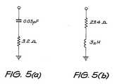
- Figure 5 shows the bi-state model of the two finger, fifty micrometer (ie, 2 by 25 ⁇ m fingers) wide HEMT used in this embodiment.
- the HEMT In the OFF state shown in figure 5(a) the HEMT is biased at zero volts. In this state the HEMT is represented by a 3.2 ohm resistor and a 0.03 picoFarad capacitor arranged in series.
- the ON state shown in figure 5(b) the HEMT is biased slightly beyond pinch-off. In this state the HEMT is represented by a 23.4 ohm resistor and a 3 nanoHenry inductance arranged in series.
- the switch is optimised using the bi-state model for a stated set of performance parameters in order to produce the required performance. Any of the parameters can, of course, be traded against other parameters to achieve different levels of performance that may be required by different applications; for instance input match could be traded against power handling capability. If the circuit were connected to a number of different circuits having different performance characteristics then it could be optimised accordingly.
Landscapes
- Electronic Switches (AREA)
- Small-Scale Networks (AREA)
Claims (10)
- Circuit de commutation multiport, comprenant : au moins trois ports (9, 10, 11) interconnectés par des lignes de transmission, les lignes de transmission étant agencées avec une bague centrale (5) et des bras s'étendant extérieurement, et les ports étant positionnés aux extrémités des bras respectifs ; un dispositif de commutation (2, 3, 4) qui est associé à chaque port, et chaque dispositif de commutation étant agencé entre la jonction d'une première (12, 13, 14) et d'une seconde (6, 7, 8) ligne de transmission, et la première ligne de transmission s'étendant entre le port et le dispositif de commutation pour fournir une adaptation d'impédance, et la seconde ligne de transmission fournissant une adaptation d'impédance et une voie de connexion vers la bague.
- Circuit de commutation multiport selon la revendication 1, dans lequel se trouve un dispositif de commutation unique (2, 3, 4) associé à chaque port.
- Circuit de commutation multiport selon la revendication 1 ou 2, dans lequel le dispositif de commutation unique (2, 3, 4) associé à chaque port est agencé pour shunter la voie de signal principale du circuit avec la voie de courant principale des dispositifs de commutation s'étendant entre la jonction des première et seconde lignes de transmission, et une terre de signalisation.
- Circuit de commutation multiport selon l'une quelconque des revendications précédentes, dans lequel les dispositifs de commutation (2, 3, 4) sont des HEMT.
- Circuit de commutation multiport selon l'une quelconque des revendications précédentes, dans lequel les dispositifs de commutation (2, 3, 4) sont agencés symétriquement autour de la bague (5).
- Procédé de construction d'un circuit de commutation multiport selon l'une quelconque des revendications précédentes, dans lequel les dimensions des lignes d'adaptation (6 à 8, 12 à 14) et des lignes qui constituent les connections vers la bague (5) sont déterminées en utilisant une procédure pour optimiser le fonctionnement du circuit comme suit :les premières (12 à 14) et les secondes (6 à 8) lignes de transmission sont choisies initialement pour avoir des longueurs d'un quart de la longueur d'onde au centre de la bande de fonctionnement du commutateur ;deux des ports (9, 10, 11) sont choisis en tant que ports d'entrée et de sortie du réseau de commutation ;les dispositifs de commutation (2, 3, 4) associés avec ces ports sont modélisés par des représentations de l'état ON ;l'autre port, ou les autres ports, sont isolés, et leurs dispositifs de commutation associés sont modélisés dans l'état OFF ; etles longueurs et les largeurs des lignes de transmission sont alors ajustées pour atteindre des paramètres de fonctionnement choisis.
- Procédé selon la revendication 6, dans lequel la procédure se poursuit en faisant varier le flux de signaux dans le circuit ; dans la première étape, les signaux fluent à partir d'un premier port vers un second port, les autres ports étant isolés ; dans la seconde étape, des signaux fluent à partir du second port vers le troisième port, les autres ports étant isolés ; et ce processus se poursuit jusqu'à ce qu'une série de paramètres optimisés soient établis pour chaque configuration de voie de signal ; la gamme de paramètres optimisés est alors examinée et une série unique des meilleurs paramètres est utilisée pour terminer la conception.
- Procédé selon la revendication 7, dans lequel les dispositifs de commutation sont modélisés dans leur état OFF par une résistance et un condensateur en série, et dans leur état ON par une résistance et une bobine d'induction montées en série.
- Circuit de commutation multiport selon la revendication 4, dans lequel l'action de commutation est obtenue en polarisant une paire de HEMT dans leur état ON afin de créer la voie de signal, tout en polarisant tous les autres HEMT dans leur état OFF ; la polarisation est appliquée aux bornes de grille des HEMT, la borne de drain est connectée à la jonction entre les premières (12 à 14) et les secondes (6 à 8) lignes de transmission et la borne de source est mise à la terre ; l'état OFF ou d'impédance faible est obtenu en appliquant une tension de CC de zéro volt à la borne de grille ; et l'état ON ou de haute impédance est obtenu en appliquant une tension de CC légèrement plus élevée que celle nécessaire pour pincer le dispositif.
- Émetteur-récepteur intégrant un dispositif de commutation multiport selon les revendications 1 à 5 ou 9.
Applications Claiming Priority (4)
| Application Number | Priority Date | Filing Date | Title |
|---|---|---|---|
| AUPO5467/97 | 1997-03-05 | ||
| AUPO5467A AUPO546797A0 (en) | 1997-03-05 | 1997-03-05 | A high frequency multi-port switching circuit |
| AUPO546797 | 1997-03-05 | ||
| PCT/AU1998/000141 WO1998039812A1 (fr) | 1997-03-05 | 1998-03-05 | Circuit de commutation multi-acces hf |
Publications (3)
| Publication Number | Publication Date |
|---|---|
| EP0902988A1 EP0902988A1 (fr) | 1999-03-24 |
| EP0902988A4 EP0902988A4 (fr) | 2001-04-11 |
| EP0902988B1 true EP0902988B1 (fr) | 2005-05-11 |
Family
ID=3799770
Family Applications (1)
| Application Number | Title | Priority Date | Filing Date |
|---|---|---|---|
| EP98905160A Expired - Lifetime EP0902988B1 (fr) | 1997-03-05 | 1998-03-05 | Circuit de commutation multi-acces hf |
Country Status (6)
| Country | Link |
|---|---|
| US (1) | US6111475A (fr) |
| EP (1) | EP0902988B1 (fr) |
| JP (1) | JP2000511033A (fr) |
| AU (1) | AUPO546797A0 (fr) |
| CA (1) | CA2251967A1 (fr) |
| WO (1) | WO1998039812A1 (fr) |
Families Citing this family (7)
| Publication number | Priority date | Publication date | Assignee | Title |
|---|---|---|---|---|
| US6600913B1 (en) * | 2000-10-27 | 2003-07-29 | Sony International (Europe) Gmbh | Two-port demodulation device |
| US7126437B2 (en) * | 2002-06-05 | 2006-10-24 | Intel Corporation | Bus signaling through electromagnetic couplers having different coupling strengths at different locations |
| WO2004100304A1 (fr) * | 2003-05-06 | 2004-11-18 | Paul Wallis | Commuteur de radio frequence et de donnees |
| US8269685B2 (en) * | 2010-05-07 | 2012-09-18 | Bae Systems Information And Electronic Systems Integration Inc. | Tapered slot antenna |
| CN108172961A (zh) * | 2017-12-21 | 2018-06-15 | 南京理工大学 | 基于半模基片集成波导的宽带Gysel型功分器 |
| CN108183302A (zh) * | 2017-12-21 | 2018-06-19 | 南京理工大学 | 基于半模基片集成波导的Gysel型功分器 |
| CN110347080B (zh) * | 2019-07-05 | 2024-07-09 | 矽杰微电子(厦门)有限公司 | 一种毫米波感应开关电路 |
Family Cites Families (8)
| Publication number | Priority date | Publication date | Assignee | Title |
|---|---|---|---|---|
| GB1578132A (en) * | 1976-05-15 | 1980-11-05 | Marconi Co Ltd | Switching arrangements |
| US4151489A (en) * | 1977-11-15 | 1979-04-24 | Communications Satellite Corporation | Waveguide switch having four ports and three connecting states |
| US4302734A (en) * | 1980-03-12 | 1981-11-24 | Nasa | Microwave switching power divider |
| GB2121239B (en) * | 1982-05-13 | 1985-10-02 | Standard Telephones Cables Ltd | A solid state changeover switch for microwave signals |
| SU1259369A1 (ru) * | 1984-12-28 | 1986-09-23 | Сибирский физико-технический институт им.В.Д.Кузнецова при Томском государственном университете им.В.В.Куйбышева | Многоканальный диодный переключатель |
| JPH08139501A (ja) * | 1994-11-04 | 1996-05-31 | Sony Corp | 伝送線路スイッチ |
| JP3332194B2 (ja) * | 1995-08-10 | 2002-10-07 | ソニー株式会社 | スイツチ半導体集積回路及び通信端末装置 |
| US5757249A (en) * | 1996-10-08 | 1998-05-26 | Lucent Technologies Inc. | Communication system having a closed loop bus structure |
-
1997
- 1997-03-05 AU AUPO5467A patent/AUPO546797A0/en not_active Abandoned
-
1998
- 1998-03-05 US US09/171,606 patent/US6111475A/en not_active Expired - Lifetime
- 1998-03-05 WO PCT/AU1998/000141 patent/WO1998039812A1/fr not_active Ceased
- 1998-03-05 CA CA002251967A patent/CA2251967A1/fr not_active Abandoned
- 1998-03-05 JP JP10537998A patent/JP2000511033A/ja active Pending
- 1998-03-05 EP EP98905160A patent/EP0902988B1/fr not_active Expired - Lifetime
Also Published As
| Publication number | Publication date |
|---|---|
| WO1998039812A1 (fr) | 1998-09-11 |
| EP0902988A1 (fr) | 1999-03-24 |
| JP2000511033A (ja) | 2000-08-22 |
| AUPO546797A0 (en) | 1997-03-27 |
| CA2251967A1 (fr) | 1998-09-11 |
| EP0902988A4 (fr) | 2001-04-11 |
| WO1998039812A8 (fr) | 1999-08-19 |
| US6111475A (en) | 2000-08-29 |
Similar Documents
| Publication | Publication Date | Title |
|---|---|---|
| CN108292911B (zh) | 低相移高频衰减器 | |
| US5808527A (en) | Tunable microwave network using microelectromechanical switches | |
| US5079527A (en) | Recombinant, in-phase, 3-way power divider | |
| US5309048A (en) | Distributed digital attenuator | |
| US6320476B1 (en) | Millimeter-band semiconductor switching circuit | |
| EP1001480B1 (fr) | Circuit à semiconducteur d'atténuation variable pour micro-ondes | |
| US7498903B2 (en) | Digital phase shifter | |
| US5148128A (en) | RF digital phase shift modulators | |
| US7157993B2 (en) | 1:N MEM switch module | |
| EP1447875A1 (fr) | Déphaseur multibit et sa méthode de fabrication | |
| US7532087B2 (en) | Switch circuit | |
| US6111475A (en) | High frequency multi-port switching circuit | |
| US7816996B2 (en) | Non-reflective MPNT switch | |
| US6580337B1 (en) | MEMS switch | |
| US5150083A (en) | Digitally controlled monolithic switch matrix using selectable dual gate FET power dividers and combiners | |
| AU734198B2 (en) | A high frequency multi-port switching circuit | |
| US5334959A (en) | 180 degree phase shifter bit | |
| US4010430A (en) | Low loss, broadband switchable microwave step attenuator | |
| US6801108B2 (en) | Millimeter-wave passive FET switch using impedance transformation networks | |
| JP4040600B2 (ja) | 2×2スイッチおよび4×4スイッチ | |
| Archer et al. | Millimetre-wave bi-directional amplifiers | |
| JPH11186803A (ja) | 高周波スイッチ回路 | |
| JP2002280811A (ja) | マイクロ波回路 | |
| US20250260391A1 (en) | Reconfigurable monolithically integrated phase-change attenuator and methods thereof | |
| JP3357715B2 (ja) | マイクロ波移相器 |
Legal Events
| Date | Code | Title | Description |
|---|---|---|---|
| PUAI | Public reference made under article 153(3) epc to a published international application that has entered the european phase |
Free format text: ORIGINAL CODE: 0009012 |
|
| AK | Designated contracting states |
Kind code of ref document: A1 Designated state(s): DK FR GB IT |
|
| 17P | Request for examination filed |
Effective date: 19990222 |
|
| A4 | Supplementary search report drawn up and despatched |
Effective date: 20010227 |
|
| AK | Designated contracting states |
Kind code of ref document: A4 Designated state(s): DK FR GB IT |
|
| GRAP | Despatch of communication of intention to grant a patent |
Free format text: ORIGINAL CODE: EPIDOSNIGR1 |
|
| GRAS | Grant fee paid |
Free format text: ORIGINAL CODE: EPIDOSNIGR3 |
|
| GRAA | (expected) grant |
Free format text: ORIGINAL CODE: 0009210 |
|
| AK | Designated contracting states |
Kind code of ref document: B1 Designated state(s): DK FR GB IT |
|
| PG25 | Lapsed in a contracting state [announced via postgrant information from national office to epo] |
Ref country code: IT Free format text: LAPSE BECAUSE OF FAILURE TO SUBMIT A TRANSLATION OF THE DESCRIPTION OR TO PAY THE FEE WITHIN THE PRE;WARNING: LAPSES OF ITALIAN PATENTS WITH EFFECTIVE DATE BEFORE 2007 MAY HAVE OCCURRED AT ANY TIME BEFORE 2007. THE CORRECT EFFECTIVE DATE MAY BE DIFFERENT FROM THE ONE RECORDED.SCRIBED TIME-LIMIT Effective date: 20050511 |
|
| REG | Reference to a national code |
Ref country code: GB Ref legal event code: FG4D |
|
| PG25 | Lapsed in a contracting state [announced via postgrant information from national office to epo] |
Ref country code: DK Free format text: LAPSE BECAUSE OF FAILURE TO SUBMIT A TRANSLATION OF THE DESCRIPTION OR TO PAY THE FEE WITHIN THE PRESCRIBED TIME-LIMIT Effective date: 20050811 |
|
| PG25 | Lapsed in a contracting state [announced via postgrant information from national office to epo] |
Ref country code: GB Free format text: LAPSE BECAUSE OF NON-PAYMENT OF DUE FEES Effective date: 20060305 |
|
| PLBE | No opposition filed within time limit |
Free format text: ORIGINAL CODE: 0009261 |
|
| STAA | Information on the status of an ep patent application or granted ep patent |
Free format text: STATUS: NO OPPOSITION FILED WITHIN TIME LIMIT |
|
| ET | Fr: translation filed | ||
| 26N | No opposition filed |
Effective date: 20060214 |
|
| GBPC | Gb: european patent ceased through non-payment of renewal fee |
Effective date: 20060305 |
|
| PGFP | Annual fee paid to national office [announced via postgrant information from national office to epo] |
Ref country code: FR Payment date: 20100324 Year of fee payment: 13 |
|
| REG | Reference to a national code |
Ref country code: FR Ref legal event code: ST Effective date: 20111130 |
|
| PG25 | Lapsed in a contracting state [announced via postgrant information from national office to epo] |
Ref country code: FR Free format text: LAPSE BECAUSE OF NON-PAYMENT OF DUE FEES Effective date: 20110331 |