EP0902990B1 - Agencement de connecteur haute densite, destine a un module pour cartes imprimees - Google Patents
Agencement de connecteur haute densite, destine a un module pour cartes imprimees Download PDFInfo
- Publication number
- EP0902990B1 EP0902990B1 EP98902384A EP98902384A EP0902990B1 EP 0902990 B1 EP0902990 B1 EP 0902990B1 EP 98902384 A EP98902384 A EP 98902384A EP 98902384 A EP98902384 A EP 98902384A EP 0902990 B1 EP0902990 B1 EP 0902990B1
- Authority
- EP
- European Patent Office
- Prior art keywords
- circuit board
- inserts
- contact tails
- arrangement
- heatsink
- Prior art date
- Legal status (The legal status is an assumption and is not a legal conclusion. Google has not performed a legal analysis and makes no representation as to the accuracy of the status listed.)
- Expired - Lifetime
Links
- 238000000034 method Methods 0.000 claims description 23
- 230000013011 mating Effects 0.000 claims description 22
- 230000000712 assembly Effects 0.000 description 25
- 238000000429 assembly Methods 0.000 description 25
- 229910000679 solder Inorganic materials 0.000 description 16
- 239000004593 Epoxy Substances 0.000 description 7
- 238000013461 design Methods 0.000 description 6
- 230000005540 biological transmission Effects 0.000 description 4
- DMFGNRRURHSENX-UHFFFAOYSA-N beryllium copper Chemical compound [Be].[Cu] DMFGNRRURHSENX-UHFFFAOYSA-N 0.000 description 3
- 230000010354 integration Effects 0.000 description 3
- 239000000463 material Substances 0.000 description 3
- RZVHIXYEVGDQDX-UHFFFAOYSA-N 9,10-anthraquinone Chemical compound C1=CC=C2C(=O)C3=CC=CC=C3C(=O)C2=C1 RZVHIXYEVGDQDX-UHFFFAOYSA-N 0.000 description 2
- 238000010276 construction Methods 0.000 description 2
- 238000005516 engineering process Methods 0.000 description 2
- 238000009434 installation Methods 0.000 description 2
- 238000004519 manufacturing process Methods 0.000 description 2
- 238000012986 modification Methods 0.000 description 2
- 230000004048 modification Effects 0.000 description 2
- 230000010287 polarization Effects 0.000 description 2
- 238000004382 potting Methods 0.000 description 2
- 238000000926 separation method Methods 0.000 description 2
- 241001136800 Anas acuta Species 0.000 description 1
- 238000013459 approach Methods 0.000 description 1
- 230000015572 biosynthetic process Effects 0.000 description 1
- 238000000576 coating method Methods 0.000 description 1
- 150000001875 compounds Chemical class 0.000 description 1
- 230000001419 dependent effect Effects 0.000 description 1
- 238000011161 development Methods 0.000 description 1
- 230000000694 effects Effects 0.000 description 1
- PCHJSUWPFVWCPO-UHFFFAOYSA-N gold Chemical compound [Au] PCHJSUWPFVWCPO-UHFFFAOYSA-N 0.000 description 1
- 239000010931 gold Substances 0.000 description 1
- 229910052737 gold Inorganic materials 0.000 description 1
- 229910052751 metal Inorganic materials 0.000 description 1
- 239000002184 metal Substances 0.000 description 1
- 238000004806 packaging method and process Methods 0.000 description 1
- 238000012856 packing Methods 0.000 description 1
- 230000001681 protective effect Effects 0.000 description 1
- 239000012858 resilient material Substances 0.000 description 1
- 230000000717 retained effect Effects 0.000 description 1
- 238000005476 soldering Methods 0.000 description 1
- 229910001220 stainless steel Inorganic materials 0.000 description 1
- 239000010935 stainless steel Substances 0.000 description 1
- 238000013519 translation Methods 0.000 description 1
Images
Classifications
-
- H—ELECTRICITY
- H01—ELECTRIC ELEMENTS
- H01R—ELECTRICALLY-CONDUCTIVE CONNECTIONS; STRUCTURAL ASSOCIATIONS OF A PLURALITY OF MUTUALLY-INSULATED ELECTRICAL CONNECTING ELEMENTS; COUPLING DEVICES; CURRENT COLLECTORS
- H01R13/00—Details of coupling devices of the kinds covered by groups H01R12/70 or H01R24/00 - H01R33/00
- H01R13/62—Means for facilitating engagement or disengagement of coupling parts or for holding them in engagement
- H01R13/629—Additional means for facilitating engagement or disengagement of coupling parts, e.g. aligning or guiding means, levers, gas pressure electrical locking indicators, manufacturing tolerances
- H01R13/631—Additional means for facilitating engagement or disengagement of coupling parts, e.g. aligning or guiding means, levers, gas pressure electrical locking indicators, manufacturing tolerances for engagement only
- H01R13/6315—Additional means for facilitating engagement or disengagement of coupling parts, e.g. aligning or guiding means, levers, gas pressure electrical locking indicators, manufacturing tolerances for engagement only allowing relative movement between coupling parts, e.g. floating connection
-
- H—ELECTRICITY
- H01—ELECTRIC ELEMENTS
- H01R—ELECTRICALLY-CONDUCTIVE CONNECTIONS; STRUCTURAL ASSOCIATIONS OF A PLURALITY OF MUTUALLY-INSULATED ELECTRICAL CONNECTING ELEMENTS; COUPLING DEVICES; CURRENT COLLECTORS
- H01R12/00—Structural associations of a plurality of mutually-insulated electrical connecting elements, specially adapted for printed circuits, e.g. printed circuit boards [PCB], flat or ribbon cables, or like generally planar structures, e.g. terminal strips, terminal blocks; Coupling devices specially adapted for printed circuits, flat or ribbon cables, or like generally planar structures; Terminals specially adapted for contact with, or insertion into, printed circuits, flat or ribbon cables, or like generally planar structures
- H01R12/50—Fixed connections
- H01R12/51—Fixed connections for rigid printed circuits or like structures
- H01R12/52—Fixed connections for rigid printed circuits or like structures connecting to other rigid printed circuits or like structures
-
- H—ELECTRICITY
- H01—ELECTRIC ELEMENTS
- H01R—ELECTRICALLY-CONDUCTIVE CONNECTIONS; STRUCTURAL ASSOCIATIONS OF A PLURALITY OF MUTUALLY-INSULATED ELECTRICAL CONNECTING ELEMENTS; COUPLING DEVICES; CURRENT COLLECTORS
- H01R12/00—Structural associations of a plurality of mutually-insulated electrical connecting elements, specially adapted for printed circuits, e.g. printed circuit boards [PCB], flat or ribbon cables, or like generally planar structures, e.g. terminal strips, terminal blocks; Coupling devices specially adapted for printed circuits, flat or ribbon cables, or like generally planar structures; Terminals specially adapted for contact with, or insertion into, printed circuits, flat or ribbon cables, or like generally planar structures
- H01R12/50—Fixed connections
- H01R12/59—Fixed connections for flexible printed circuits, flat or ribbon cables or like structures
- H01R12/62—Fixed connections for flexible printed circuits, flat or ribbon cables or like structures connecting to rigid printed circuits or like structures
-
- H—ELECTRICITY
- H01—ELECTRIC ELEMENTS
- H01R—ELECTRICALLY-CONDUCTIVE CONNECTIONS; STRUCTURAL ASSOCIATIONS OF A PLURALITY OF MUTUALLY-INSULATED ELECTRICAL CONNECTING ELEMENTS; COUPLING DEVICES; CURRENT COLLECTORS
- H01R12/00—Structural associations of a plurality of mutually-insulated electrical connecting elements, specially adapted for printed circuits, e.g. printed circuit boards [PCB], flat or ribbon cables, or like generally planar structures, e.g. terminal strips, terminal blocks; Coupling devices specially adapted for printed circuits, flat or ribbon cables, or like generally planar structures; Terminals specially adapted for contact with, or insertion into, printed circuits, flat or ribbon cables, or like generally planar structures
- H01R12/70—Coupling devices
- H01R12/71—Coupling devices for rigid printing circuits or like structures
- H01R12/72—Coupling devices for rigid printing circuits or like structures coupling with the edge of the rigid printed circuits or like structures
- H01R12/721—Coupling devices for rigid printing circuits or like structures coupling with the edge of the rigid printed circuits or like structures cooperating directly with the edge of the rigid printed circuits
-
- H—ELECTRICITY
- H05—ELECTRIC TECHNIQUES NOT OTHERWISE PROVIDED FOR
- H05K—PRINTED CIRCUITS; CASINGS OR CONSTRUCTIONAL DETAILS OF ELECTRIC APPARATUS; MANUFACTURE OF ASSEMBLAGES OF ELECTRICAL COMPONENTS
- H05K1/00—Printed circuits
- H05K1/02—Details
- H05K1/11—Printed elements for providing electric connections to or between printed circuits
- H05K1/117—Pads along the edge of rigid circuit boards, e.g. for pluggable connectors
-
- H—ELECTRICITY
- H05—ELECTRIC TECHNIQUES NOT OTHERWISE PROVIDED FOR
- H05K—PRINTED CIRCUITS; CASINGS OR CONSTRUCTIONAL DETAILS OF ELECTRIC APPARATUS; MANUFACTURE OF ASSEMBLAGES OF ELECTRICAL COMPONENTS
- H05K1/00—Printed circuits
- H05K1/02—Details
- H05K1/14—Structural association of two or more printed circuits
- H05K1/141—One or more single auxiliary printed circuits mounted on a main printed circuit, e.g. modules, adapters
Definitions
- This invention relates to an electrical connector arrangement for a circuit board package, and to a method of assembling electrical connectors to a circuit board. More specifically the invention relates to an arrangement and method for increasing the spacing between contact tails extending from edge connectors of a circuit board module at the point of electrical interconnection between the circuit board and the contact tails.
- LRM is a standardized electrical connector which contains several hundred electrical contacts arranged in multiple rows, each contact having a solder tail connected to a pad on a circuit board, the circuit board being situated within a chassis or rack.
- LRMs serve as circuit modules for aircraft flight control circuitry, and include connectors for interconnecting flight control circuitry situated in separate modules arranged to be mounted in a chassis or rack and interconnected via mating connectors affixed to the backplane of the chassis or rack and buses or cables designed to carry high baud rate digital transmissions to and from the control circuits.
- the standard LRM configurations are no longer capable of reliably providing the required number of input/output lines.
- the number of required input/output lines currently approaches 500, which is not possible in existing LRM configurations without sacrificing electrical performance and reliability or increasing the size of the interface connectors for the circuit module.
- the main reason that the number of contacts is limited is not the size or arrangement of the contacts in the module connectors, but rather difficulties in electrically connecting the contacts to the circuit boards in the module. While the number of contacts in the connector itself can been increased by increasing the number of rows and using different length contact tails to reach the circuit board, all of the contacts must still be connected to the circuit board itself.
- these configurations lack sufficient dimensional misalignment compensation or compliance in the contacts to compensate for tolerances in mounting the connector assemblies on the backplane and for float which occurs in conductively cooled modules after the modules have been mated to the backplane and the heatsink is translated normal to the plane of the heatsink until its edges are in intimate contact with the cold walls of a rack or chassis in which the module is mounted.
- Termination of the connector contacts to the circuit board package is by means of relative long and thin surface mount leads 7 extending from connectors 11 and 12.
- the leads are formed into a compliant state with the mating ends of the contacts (not shown) being staggered to provide increased contact density within the connector.
- the compliant form of the contacts permits the contacts to absorb dimensional differences between the connector and the board package. Examples of this type of arrangement are illustrated in U.S. Patent Nos. 4,734,042 (Martens et al .), 4,808,115 (Norton et al .), 5,090,116 ( Henschen et al .), and 5,090,911 (Welsh).
- the invention provides a connector arrangement in which the tails of contacts in the connector are not terminated to pads or terminals on the main circuit board, but rather are terminated to pads or terminals on pairs of intermediate circuit boards connected to the main boards, the intermediate circuit boards each providing two termination surfaces rather than one, thereby effectively doubling the space available for termination.
- the tails of the contacts are solder tails which are surface mounted to the intermediate circuit boards, and the intermediate circuit boards are electrically connected to the main circuit boards by a rigid-flex connection in which the rigid main and intermediate circuit boards are linked by flexible portions carrying traces extending from the main circuit board.
- the main circuit boards form a standard circuit board package comprised of a heatsink and two circuit boards.
- connection arrangement and method of the preferred embodiments of the invention provides an improved solder tail structure in which the tails are relatively short and stiff in comparison with those of conventional arrangements, and of equal length despite the connector having four rows of contacts, thereby improving the electrical performance and reliability of the contacts without limiting float.
- Float is permitted by the flexible connections between the intermediate and main circuit boards.
- the uniform line lengths resulting from solder tails of the same length and configuration mean equal propagation delay, equal line resistance, and equal line inductance.
- the rigid-flex arrangement can be designed to bring transmission line structures closer to the backplane, minimizing the mismatch zone, and offering the possibility of wider or shunted traces for the transmission of high currents.
- Additional features of the connector arrangement and method of the preferred embodiments of the invention include the use of a conventional dielectric insert in which the contacts are positioned and bonded by epoxy, formation of the tails of the contacts in a uniform J-shape to accept the intermediate circuit boards like a conventional card edge connector, the addition of tower features to the dielectric insert to guide and position the intermediate circuit board package relative to the dielectric insert, and stacking of multiple dielectric inserts within a common electrostatic discharge (ESD) shield having a non-conductive outer layer to hold the inserts together, thereby providing a connector which is easier to manufacture, easier to terminate to LRMs, and also electrically superior because each connector has been designed with equal path lengths for each row of contacts.
- ESD electrostatic discharge
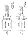
- the connector termination arrangement of the preferred embodiment of the invention includes a circuit board package made up of a pair of printed circuit boards 8 and 9 attached to a frame or heatsink 10, and a pair of connector insert assemblies 11 and 12 each housing a plurality of mating contacts, the tails 13 of which are to be electrically connected to the circuit boards 8 and 9.
- the termination arrangement of this embodiment makes use of a pair of rigid intermediate circuit boards 14 and 15 connected to the main printed circuit boards by flexible circuit board interconnecting portions 16 and 17.
- circuit board arrangement of this most general embodiment of the invention makes use of an existing circuit board technology referred to by those skilled in the art as a "rigid-flex" circuit board construction, in which the flexible sections 16 and 17 are in the form of multiple printed circuit layers which are extensions of corresponding layers in main circuit boards 8 and 9 to form flexible interconnecting portions between the main circuit board and the intermediate or secondary circuit boards.
- a rigid-flex circuit board construction in which the flexible sections 16 and 17 are in the form of multiple printed circuit layers which are extensions of corresponding layers in main circuit boards 8 and 9 to form flexible interconnecting portions between the main circuit board and the intermediate or secondary circuit boards.
- the point of the invention is of course to provide dual-sided terminations on the intermediate circuit boards even though each of the main circuit boards has only one available surface, the other surface being unusable because it is in contact with the frame 10, described below as being in the form of a heatsink.
- the terminations can thus take a variety of forms, including various pin tail configurations, although the illustrated embodiment uses J-shaped surface mount contact tails 13.
- Figures 1 and 2 are for purposes of illustrated the basic principles of the invention, and in particular the principle of increasing the spacing of contact terminations to circuit boards by adding intermediate circuit boards, and that no materials or structural details of the circuit boards 8, 14, and 16, frame 10, and insert assemblies 11 have been included in these Figures because the circuit boards can be made of a variety of materials, including layered structures, while the frame 10 does not necessarily need to be a heatsink as described in connection with more specific embodiments of the invention, and the insert assemblies can represent a variety of different connector structures.
- FIG. 3-12 A preferred embodiment of the invention which implements the principles illustrated in Figure 2 is shown in Figures 3-12. Although represented as an SEM-E type circuit board module, it should of course be recognized that the principles of the invention may be applied in contexts other than the specific type of module shown.
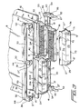
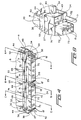
- the overall layout of the preferred module is best illustrated in Figures 3-5.
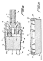
- the circuit board package comprised of main circuit boards 8 and 9 is arranged such that the heat sink 10 extends forwardly of the main circuit boards, with the intermediate circuit boards 14 and flexible circuit board sections 16 being positioned above and below the heatsink 10 in the manner best illustrated in Figure 5.
- the contact tails 13 which interface with the rigid-flex intermediate printed circuit boards 16 are short, radiused, surface mount tails extending rearwardly from the mating portions 18 of the contacts, and are preferably composed of a high conductivity resilient material such as beryllium copper, having a rectangular cross-section.
- These contact tails 13 have a smaller width than the mating sections 18 of the contacts and may advantageously be situated eccentrically with respect to the mating sections to achieving a narrower or nearly planar orientation of corresponding pairs for mating with opposite sides of each circuit board while providing an inward bias relative to the intermediate circuit boards in order to provide a centering effect.
- the contacts are thus preferably positioned within passages 19 of the dielectric inserts 20 and 21 before termination of the contacts so that the solder tails 13 are aligned to engage corresponding pads on the intermediate circuit boards 14 and 15.
- the contacts may be bonded by epoxy.
- the epoxy has the advantage of not only retaining the contacts in the dielectric inserts, but also seals the rear surface of the inserts, so that foreign materials such as conformal coatings cannot invade the contacts.
- the intermediate circuit boards 14 and 15 may be advantageous guided into position relative to the dielectric insert pairs 20A,20B and 21A,21B, prior to termination, by slots 28 in extensions 27 to provide a self fixturing arrangement which simplifies termination of the contacts tails to the circuit board.
- slots 28 in extensions 27 to provide a self fixturing arrangement which simplifies termination of the contacts tails to the circuit board.
- the intermediate circuit boards and the dielectric inserts may have keying features (not shown) for keying and/or polarizing the assembly to ensure correct assembly by, for example, varying the shape of the slots 28 and including asymmetric structures on the portions of the intermediate circuit boards which fit into the slots.
- the printed circuit boards can be bonded to the dielectric inserts with epoxy, thereby providing a mechanical bond between the printed circuit boards and the insert assemblies, isolating the surface mount tails and solder joints from mechanical stress.
- the solder tails and terminations may be further protected at this point by enclosure within a protective sleeve and potting the structure, so long as the coefficient of thermal expansion of the potting compound matches that of the printed circuit board.
- all of the surface mount tails are arranged to have essentially the same length, which has the advantage of minimizing impedance variations.
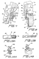
- the relatively short length of the solder tails may enable alignment to be maintained between the contacts and the solder pads or terminals on the circuit board prior to termination without the need for tie bars, although tie bars 26 can still be utilized if desired as illustrated in Figures 6 and 11.
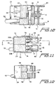
- an especially advantageous type of contact is the type of brush contact represented respectively in Figures 13A and 13B by female contact 18' and male contact 18", which have the advantage of a low mating force.
- This type of contact consists of seven 0.007 diameter, gold-plated, beryllium-copper wires 180 crimped into a bundle, the exposed tips 181 of the seven wires being cleaved at a precise angle to create seven extremely sharp points which collectively form a hermaphroditic contact.
- the brush contacts are protected by stainless steel sleeves which serve to protect the brush interface from damage and provide a surface to push on the contacts to seat them in the insert.
- the contacts may be stabilized in the insert assemblies via a detent 182.
- the preferred embodiment provides various improvements in the connector structure, the shield and ground structure, and the overall module arrangement. These improvements include the provision of flange 27 on the dielectric inserts, which includes slots 28 for supporting the intermediate circuit boards during termination, and the inclusion of a unique shielding/grounding structure made up of shields 24,25 and shell blocks 36,37 arranged to permit the module to be assembled together and grounded, following termination and movement of the dielectric housings into position, simply by inserting the shields over the dielectric inserts, positioning flanges 27' on the shell blocks such that flanges 27 on the inserts and 27" on the shields are retained between flanges 27' and the heatsink, and fastening the shell blocks to the heatsink.
- the overall configuration of the dielectric inserts 20A,20B,21A,21B is best seen from Figures 3, 5, and 6.
- the portion of the inserts which contain passages 19 is conventional in shape, with extensions 27 extending rearwardly from the contact containing portions and also to the side, as best shown in Figure 6.
- the rear inside portions of the extensions 27 contain slots 28 for guiding and position the intermediate circuit boards, including polarization features if desired, while the front portion of the extensions 27 form a surface 33 against which flange 27" of the shields 24 and 25 are captured by flange 27' after positioning of the shell blocks 36 and 37 as shown in Figure 8.
- slots 28 may include rails 29 to help keep the intermediate circuit board within the slots, and which can also serve as keying or polarization features if asymmetrically arranged, while notches 30 and 31 (the later shown only in Figures 5 and 11) may be formed respectively on the upper side of extensions 27 of lower inserts 21A,21B and on the lower side of extensions 27 of upper inserts 20A,20B to provide clearance for heat sink 10 when the upper and lower inserts are brought together.
- the ESD shields 24 and 25 illustrated in Figures 3-5 and 9 not only serve to intercept ESD before it can find its way to a brush contact by forming a Faraday cage structure, but also holds together the insert assemblies which make up the insert bays of the connector/circuit board module, and are the second feature of the module to interface with the backplane connector during mating.
- each shield includes a main portion 70 including side walls 71, upper and lower walls 72 which fit over and holds together respective pairs 20A, 20B and 21A, 21B of upper and lower inserts, the above-described flanges 27", and front walls 73 including the above-described openings 19' to permit entry of contacts of the mating backplane connectors, as well as rearward extensions 74 section for engaging shell blocks 36 and 37.
- the metal shell block 36 includes tower portions 38-40 and the lower shell block 37 includes portions 41-43 which serve both to capture flanges 27" of shields 24 and 25 against front surfaces 33 of dielectric insert extensions 27, and also to attach the shell blocks to heatsink 10. Capture of the shield flanges is accomplished by flanges 27' which extend inwardly from the front side of the tower structures 38-40 and lower shell block portions 41-43, while connection to the heatsink is by means of locking members 46 which pass through openings 44 situated towards the rear of tower portions 38-40 and through threaded holes 45 in portions 41-43 so as to lock the heatsink between lower surfaces 47 of upper shell block 36 and upper surfaces 48 of lower shell block 37. Because the shields and inserts are captured only from the front side, it will be appreciated that the illustrated structure will hold the shields and inserts against movement in the plane of the circuit board while advantageously permitting movement in the vertical directions to permit float, as discussed above.
- shell blocks 36 and 37 include cover mounting extensions 49, which form a shelf for mounting of module cover members 60 and 61, and which include screw holes 50 for cover mounting screws 51, as well as openings or pockets 34 for replaceable connector keying, and openings for guide/ground pins 52.
- the shell blocks as illustrated thus serve to retain the insert assemblies and ESD shields together and lock them to the heatsink, while at the same time permitting vertical movement of the shields and inserts relative to the heat sink and main circuit boards, and providing a ground path from the cover, shields, and ground pins to the heatsink.
- the shell blocks 36 and 37 are illustrated as being continuous structures, including connecting sections 53 and 55, one or both of shell blocks 36 and 37 could also be made of separate structures corresponding to the respective portions 38-40 and 41-43.
- the guide pins 52 are the first feature of the completed module to engage the backplane connector during installation of the module in a chassis or rack, serving to provide an amount of radial pickup to initiate engagement and, when engaged with the backplane connector, to provide low resistance engagement between the shields 24 and 25 of the module, via flanges 27" and shell blocks 36 and 37, and the mating backplane connectors.
- the pins are composed of gold plated, hard beryllium-copper but are designed so that if they are mis-handled they will break rather than bend so as to the prevent connectors from being damaged during mating due to bent guide/ground pins.
- each of the openings 34 accommodates two keys 340 having an eccentrically positioned extension 341 which defines the corresponding key receiving opening, with each of the four keys being settable in four different positions by rotating a base portion 342 of the keys within a retaining member 343, for a total of 256 different keyhole combinations. Unless the chassis has more than 256 module slots, this is sufficient to ensure that each module will only be able to be connected to the proper slot.
- cover members 60 and 61 may extend rearwardly to completely enclose the circuit board package, and that the dimensions and exterior configuration of the module should be the same as those of the conventional module which the present invention is designed to replace so that, from the outside, the preferred module is indistinguishable from the conventional module except with respect to the number of contact pins in the backplane connectors.
- the module illustrated in Figures 2-13 provides an arrangement in which termination of the module circuit board to the connector contacts via a rigid-flex printed circuit board has been greatly simplified.
- the contacts of the individual inserts straddle the printed circuit board and are formed to compress the board like a card-edge connector.
- the slots at each end of the dielectric inserts guide the rigid interface board of the rigid-flex into the correct position for termination, while self-fixturing of the inserts is made possible because of the wider pitch of the surface mount leads.
- the insert assemblies are mounted to the rigid-flex printed circuit board prior to the attachment of the printed circuit board to the heatsink, so as to minimize A and B side registration problems, and the insert assemblies are subsequently brought together and secured by first fitting the shields over the insert assemblies and then mounting the shell blocks on the heatsink in a position which captures and locks both the shells and the insert assemblies into position relative to the heatsink and circuit boards.
- the mating sections 18 of the contacts are positioned within openings 19 in dielectric inserts 20 and 21, the contacts are bonded by epoxy.
- the intermediate circuit boards 14 and 15 are then positioned within slots 28 relative to the rows of contact tails 13, before the heatsink 10 has been placed in its final position, and the tails are soldered into position.
- the intermediate circuit boards are bonded to the dielectric insert with epoxy, and the surface mount tails are optionally potted to complete the termination procedure.
- circuit card assemblies made up of the contacts, intermediate circuit boards and dielectric inserts may then, in the illustrated embodiment, be positioned relative to the main circuit boards and heatsink, making use of the flexibility of the flexible portions 16 of the package, so that quarter insert assemblies or half bays 20A,20B,21A,21B come together with the circuit boards to make complete bays, with surfaces 30 and 31 of extensions 27 forming guide slots for the heatsink.
- the ESD shields 24 and 25 are then carefully installed to hold the insert assemblies together in a vertical direction.
- the assemblies After the insert assemblies have been terminated to the intermediate circuit boards and the ESD shields assembled over the insert assembly, the assemblies straddle the heatsink in roughly their final position.
- the upper and lower shell blocks 36 and 37 can then be slid into position from above and below the ESD shields 24 and 25, down along the vertical axis, and the three locking members are then installed from the upper shell block through the heatsink into the lower shell block while a vertical force is applied to the shell blocks as necessary to keep the plastic extensions of the dielectric inserts flush to the edge of the heatsink, and finally the entire assembly may optionally be vacuum baked to any epoxy which has been applied to the various parts to assist in fixing the parts following positioning.
- the rigid-flex concept could also be used to flexibly connect multiple intermediate circuit boards to the main circuit board or boards, and/or that additional flexible sections could be provided to connect intermediate circuit boards with sub-intermediate circuit boards, further increasing the available contact termination space.
Landscapes
- Coupling Device And Connection With Printed Circuit (AREA)
Claims (23)
- Agencement destiné à raccorder électriquement une pluralité de bouts (13) de contact à des composants sur une carte à circuit imprimé, dans lequel la carte à circuit imprimé comprend une carte (8, 9) à circuit imprimé principale rigide sur une surface sur laquelle sont montés des composants électroniques, caractérisé en ce qu'il comprend :une carte (14, 15) à circuit imprimé intermédiaire rigide ayant deux surfaces principales se faisant face en opposition, un premier groupe desdits bouts de contact se terminant sur une première parmi lesdites deux surfaces et un second groupe desdits bouts de contact se terminant sur une seconde parmi lesdites deux surfaces ; etune section souple (16, 17) s'étendant entre ladite carte (8, 9) à circuit imprimé principale et ladite carte (14, 15) à circuit imprimé intermédiaire ou interconnectant électriquement lesdits bouts (13) de contact dans chacun parmi lesdits deux groupes auxdits composants sur ladite une surface de la carte (8, 9) à circuit imprimé principale.
- Agencement selon la revendication 1, dans lequel lesdits bouts de contact se terminent sur ladite carte à circuit imprimé intermédiaire par un montage en surface.
- Agencement selon la revendication 1, comprenant en outre une seconde carte à circuit imprimé principale ayant une surface sur laquelle des composants électroniques sont montés, une seconde carte à circuit imprimé intermédiaire ayant deux surfaces principales sur lesquelles des bouts de contact se terminent, une seconde section souple entre ladite seconde carte à circuit imprimé principale et ladite seconde carte à circuit imprimé intermédiaire, et un dissipateur thermique (10) intercalé entre lesdites première et seconde cartes à circuit imprimé principales.
- Agencement selon la revendication 3, dans lequel lesdits bouts de contact s'étendent depuis des contacts positionnés à l'intérieur de passages dans des inserts diélectriques (20A, 20B, 21A, 21B) de connecteurs électriques.
- Agencement selon la revendication 4, dans lequel lesdits bouts de contact s'étendent de manière excentrique depuis lesdits contacts de telle manière que des paires de bouts de contact supérieurs inférieurs sont quasi planaires.
- Agencement selon la revendication 4, dans lequel lesdits inserts diélectriques comportent des extensions ayant des fentes (28) destinées à guider lesdites cartes à circuit imprimé intermédiaires entre des rangées de bouts de contact supérieurs et inférieurs.
- Agencement selon la revendication 6, dans lequel une surface supérieure d'une extension sur un insert inférieur parmi lesdits inserts fait face à une surface inférieure sur une extension d'un insert supérieur parmi lesdits inserts afin d'intercaler ledit dissipateur thermique (10) lorsque ledit insert supérieur est déplacé verticalement, relativement audit insert inférieur.
- Agencement selon la revendication 7, comprenant en outre un dispositif de protection (24, 25) de décharges électrostatiques entourant des surfaces supérieures, latérales et avant desdits inserts.
- Agencement selon la revendication 8, comprenant en outre des blocs (36, 37) d'enveloppe supérieur et inférieur positionnés de telle manière que des collerettes sur lesdits blocs d'enveloppe capturent lesdites extensions des inserts diélectriques et des collerettes sur lesdits dispositifs de protection et bloquent les inserts et les dispositifs de protection sur le dissipateur thermique (10) lorsque les blocs d'enveloppe sont fixés sur le dissipateur thermique.
- Agencement selon la revendication (9), comprenant en outre un couvercle solidement fixé sur lesdits blocs d'enveloppe destiné à enfermer lesdites cartes à circuit imprimé et à former un module de carte à circuit imprimé électronique destiné à être monté dans une baie, lesdits connecteurs étant agencés afin de s'apparier avec des connecteurs homologues sur une plaque de raccordement arrière de ladite baie.
- Agencement selon la revendication 10, dans lequel des blocs d'enveloppe mettent à la masse ledit couvercle et lesdits dispositifs de protection sur ledit dissipateur thermique, et dans lequel des forces appliquées sur lesdits contacts au cours d'un appariement sont transmises au travers desdits inserts et des blocs d'enveloppe audit dissipateur thermique.
- Agencement selon la revendication 10, comprenant en outre des poches dans l'un desdits blocs d'enveloppe pour contenir des éléments de déclenchement, et des ouvertures destinées à comporter des doigts de guidage afin de fixer solidement lesdits connecteurs dudit module sur lesdits connecteurs homologues, lesdits doigts de guidage étant également mis à la terre sur ledit dissipateur thermique par le biais desdits blocs d'enveloppe.
- Agencement selon la revendication 7, comprenant en outre des blocs d'enveloppe supérieur et inférieur positionnés de telle manière que des collerettes sur lesdits blocs d'enveloppe capturent lesdites extensions des inserts diélectriques et bloquent les inserts sur le dissipateur thermique lorsque les blocs d'enveloppe sont fixés sur le dissipateur thermique.
- Agencement selon la revendication 4, comprenant en outre un dispositif de protection de décharge électrostatique entourant des surfaces supérieures, latérales et avant desdits inserts.
- Agencement selon la revendication 14, comprenant en outre des blocs d'enveloppe supérieur et inférieur positionnés de telle manière que des collerettes sur lesdits blocs d'enveloppe capturent lesdites extensions des inserts diélectriques et des collerettes sur lesdits dispositifs de protection et verrouille les inserts et les dispositifs de protection sur le dissipateur thermique lorsque les blocs d'enveloppe sont fixés sur le dissipateur thermique.
- Procédé consistant à raccorder électriquement des bouts (13) de contact sur une carte (8, 9) à circuit imprimé principale ayant une surface sur laquelle sont montés des composants électroniques, comprenant les étapes consistant à :amener un premier groupe de bouts (13) de contact à se terminer sur une première surface principale d'une carte (14, 15) à circuit imprimé intermédiaire et amener un second groupe des bouts (13) de contact à se terminer sur une seconde surface principale de la carte (14, 15) à circuit imprimé intermédiaire, ladite carte (14, 15) à circuit imprimé intermédiaire étant raccordée à la carte (8, 9) à circuit imprimé principale par une section (16, 17) d'interconnexion souple, moyennant quoi lesdits bouts de contact desdits premier et second groupes sont ainsi interconnectés électriquement avec lesdits composants électroniques sur ladite une surface de la carte à circuit imprimé principale.
- Procédé selon la revendication 16, dans lequel l'étape consistant à raccorder électriquement les bouts de contact comprend l'étape de montage en surface des bouts de contact sur ledit côté opposé de ladite carte (14, 15) à circuit imprimé intermédiaire.
- Procédé selon la revendication 17, comprenant en outre les étapes consistant à positionner des contacts sur lesquels les bouts de contact sont fixés dans des ouvertures dans un insert diélectrique d'un connecteur, et à positionner la carte à circuit imprimé intermédiaire dans une fente dans ledit insert au cours d'un raccord électrique des bouts de contact sur les côtés opposés de la carte à circuit imprimé intermédiaire.
- Procédé selon la revendication 18, comprenant en outre l'étape consistant à amener des rangées supplémentaires de bouts de contact fixés sur des contacts positionnés dans des ouvertures dans un second insert diélectrique à se terminer sur des côtés opposés d'une seconde carte à circuit imprimé intermédiaire raccordée à une seconde carte à circuit imprimé principale par une seconde section d'interconnexion souple, un dissipateur thermique planaire s'intercalant entre lesdites première et seconde cartes à circuit imprimé principales.
- Procédé selon la revendication 19, comprenant en outre l'étape consistant à déplacer verticalement lesdits premier et second inserts diélectriques l'un vers l'autre à la suite de l'étape consistant à amener les bouts de contact à se terminer sur lesdites cartes à circuit imprimé intermédiaires.
- Procédé selon la revendication 20, comprenant en outre l'étape consistant à ajuster un dispositif de protection de décharge électrostatique au-dessus desdits éléments diélectriques après que lesdits éléments diélectriques ont été rassemblés.
- Procédé selon la revendication 21, comprenant en outre les étapes consistant à positionner les blocs d'enveloppe de telle manière que des extensions desdits éléments diélectriques capturent des collerettes sur ledit dispositif de protection, contre ledit dissipateur thermique, et ultérieurement, fixer lesdits blocs d'enveloppe sur ledit dissipateur thermique.
- Procédé selon la revendication 22, comprenant en outre l'étape consistant à attacher des éléments de couvercle sur lesdits blocs d'enveloppe afin de former un module de carte à circuit imprimé agencé afin d'être monté à l'intérieur d'une baie, ledit connecteur étant agencé afin de s'apparier avec un connecteur homologue sur une plaque de raccordement arrière de ladite baie.
Applications Claiming Priority (3)
| Application Number | Priority Date | Filing Date | Title |
|---|---|---|---|
| US782792 | 1997-01-13 | ||
| US08/782,792 US5947753A (en) | 1997-01-13 | 1997-01-13 | High density connector arrangement for a circuit board module |
| PCT/US1998/000032 WO1998031075A1 (fr) | 1997-01-13 | 1998-01-13 | Agencement de connecteur haute densite, destine a un module pour cartes imprimees |
Publications (3)
| Publication Number | Publication Date |
|---|---|
| EP0902990A1 EP0902990A1 (fr) | 1999-03-24 |
| EP0902990A4 EP0902990A4 (fr) | 2000-03-15 |
| EP0902990B1 true EP0902990B1 (fr) | 2006-05-24 |
Family
ID=25127195
Family Applications (1)
| Application Number | Title | Priority Date | Filing Date |
|---|---|---|---|
| EP98902384A Expired - Lifetime EP0902990B1 (fr) | 1997-01-13 | 1998-01-13 | Agencement de connecteur haute densite, destine a un module pour cartes imprimees |
Country Status (5)
| Country | Link |
|---|---|
| US (1) | US5947753A (fr) |
| EP (1) | EP0902990B1 (fr) |
| CA (1) | CA2248712C (fr) |
| DE (1) | DE69834606T2 (fr) |
| WO (1) | WO1998031075A1 (fr) |
Families Citing this family (32)
| Publication number | Priority date | Publication date | Assignee | Title |
|---|---|---|---|---|
| JP2000068007A (ja) | 1998-08-20 | 2000-03-03 | Fujitsu Takamisawa Component Ltd | ケーブル付き平衡伝送用コネクタ |
| DE19859228C1 (de) * | 1998-12-21 | 2000-06-21 | Siemens Nixdorf Banking Syst | Steckbare Leiterplatte mit beweglicher Steckkontaktanordnung |
| US6450822B1 (en) * | 1999-06-01 | 2002-09-17 | Rockwell Collins, Inc. | System and method for electrically and mechanically coupling an avionics line replaceable unit with electronic equipment |
| TW452235U (en) * | 2000-09-29 | 2001-08-21 | Hon Hai Prec Ind Co Ltd | Connection device of electronic card |
| FR2816066B1 (fr) * | 2000-10-26 | 2003-01-03 | Framatome Connectors Int | Module de connexion electro-optique |
| JP3437837B2 (ja) * | 2001-02-02 | 2003-08-18 | 株式会社東芝 | フレキシブルプリント回路基板用コネクタ、これを備えたヘッドアクチュエータ、および磁気ディスク装置 |
| US6419502B1 (en) * | 2001-03-14 | 2002-07-16 | Hon Hai Precision Ind. Co., Ltd. | Electrical connector assembly with improved contact arrangement |
| US7073954B1 (en) | 2001-09-17 | 2006-07-11 | Stratos International, Inc. | Transceiver assembly for use in fiber optics communications |
| US7056032B2 (en) * | 2001-09-17 | 2006-06-06 | Stratos International, Inc. | Transceiver assembly for use in fiber optics communications |
| US7073955B1 (en) | 2001-09-17 | 2006-07-11 | Stratos International, Inc. | Transceiver assembly for use in fiber optics communications |
| US6842325B2 (en) * | 2001-09-19 | 2005-01-11 | Square D Company | Flexible circuit adhered to metal frame of device |
| US6674644B2 (en) * | 2001-11-01 | 2004-01-06 | Sun Microsystems, Inc. | Module and connector having multiple contact rows |
| US7473931B1 (en) | 2002-02-28 | 2009-01-06 | Garmin International, Inc. | System and method for mounting units for an avionic display |
| US7008233B1 (en) | 2002-02-28 | 2006-03-07 | Garmin, Ltd. | Retractable panel interface cable device and method |
| US6549424B1 (en) | 2002-02-28 | 2003-04-15 | Garmin Ltd. | Electronic equipment module mounting apparatus and method |
| US6589061B1 (en) * | 2002-03-07 | 2003-07-08 | Hon Hai Precision Ind. Co., Ltd. | Printed circuit board for straddle mount electrical connector and method for pasting the same |
| US6903934B2 (en) * | 2002-09-06 | 2005-06-07 | Stratos International, Inc. | Circuit board construction for use in small form factor fiber optic communication system transponders |
| CN1318823C (zh) * | 2002-09-20 | 2007-05-30 | 矢崎总业株式会社 | 文字板组件及其制造方法 |
| DE10261410B4 (de) * | 2002-12-30 | 2008-09-04 | Qimonda Ag | Verfahren zur Verbindung einer integrierten Schaltung mit einem Substrat und entsprechende Schaltungsanordnung |
| US7248455B2 (en) * | 2003-10-31 | 2007-07-24 | International Business Machines Corporation | Method and apparatus for providing compressive connection with electrostatic discharge dissipative properties |
| US7355857B2 (en) | 2006-02-07 | 2008-04-08 | Methode Electronics, Inc. | Heat sink gasket |
| US7453690B2 (en) * | 2006-09-27 | 2008-11-18 | International Business Machines Corporation | Electronic component interconnection and assembly |
| CN101232131B (zh) * | 2007-01-22 | 2010-06-23 | 富士康(昆山)电脑接插件有限公司 | 电连接器组件 |
| JP5297326B2 (ja) * | 2009-10-08 | 2013-09-25 | 富士通コンポーネント株式会社 | 雄コネクタ、コネクタ及びバックプレーン |
| US8517759B1 (en) * | 2011-02-15 | 2013-08-27 | Blue Sun Energy, Inc. | Ribbon flex light connector system |
| US9078569B2 (en) * | 2012-08-20 | 2015-07-14 | Zhengrong Ying | Configurable data measurement and acquisition systems for multi-slice X-ray computed tomography systems |
| US9093764B2 (en) | 2013-01-17 | 2015-07-28 | Cooper Technologies Company | Electrical connectors with force increase features |
| US8926360B2 (en) | 2013-01-17 | 2015-01-06 | Cooper Technologies Company | Active cooling of electrical connectors |
| EP2821988A1 (fr) * | 2013-07-02 | 2015-01-07 | Samsung Electronics Co., Ltd | Connecteur pour réduire la paradiaphonie |
| EP3843222B1 (fr) * | 2019-12-24 | 2025-02-26 | Fico Triad, S.A. | Connecteur électrique |
| US11757221B2 (en) * | 2021-11-02 | 2023-09-12 | Te Connectivity Solutions Gmbh | Electrical connector having contact modules |
| US20250383390A1 (en) * | 2024-06-12 | 2025-12-18 | RSD Aviation Patent, LLC | Signal access extender apparatus |
Family Cites Families (23)
| Publication number | Priority date | Publication date | Assignee | Title |
|---|---|---|---|---|
| US3492538A (en) * | 1967-09-07 | 1970-01-27 | Thomas & Betts Corp | Removable stack interconnection system |
| FR2310641A1 (fr) * | 1975-05-05 | 1976-12-03 | Amp Inc | Procede de fabrication d'un connecteur electrique |
| DE2901416A1 (de) * | 1979-01-15 | 1980-07-24 | Vdo Schindling | Anordnung zum elektrischen verbinden einer vielzahl von anschluessen |
| US4425015A (en) * | 1980-05-29 | 1984-01-10 | Texas Instruments Incorporated | Attachable, circuit-terminating, circuit board edge member |
| US4682828A (en) * | 1985-12-06 | 1987-07-28 | 501 Woven Electronics Corporation | Bus bar bridged pc board for transitional termination of multiple cables and method |
| US4708659A (en) * | 1986-08-25 | 1987-11-24 | Zenith Electronics Corporation | PC board connector with shorting bus bar |
| US4734042A (en) * | 1987-02-09 | 1988-03-29 | Augat Inc. | Multi row high density connector |
| US4808115A (en) * | 1987-07-28 | 1989-02-28 | Amp Incorporated | Line replaceable connector assembly for use with printed circuit boards |
| US4992052A (en) * | 1988-02-01 | 1991-02-12 | E. I. Du Pont De Nemours And Company | Modular connector system with high contact element density |
| US4997379A (en) * | 1988-10-06 | 1991-03-05 | Rozmus John J | Electrical contacts |
| JPH02250388A (ja) * | 1989-03-24 | 1990-10-08 | Nec Corp | 混成集積回路 |
| US4913656A (en) * | 1989-04-07 | 1990-04-03 | Rogers Corporation | Electrical connector |
| US5090911A (en) * | 1990-01-11 | 1992-02-25 | Itt Corporation | Modular connector system |
| US5024607A (en) * | 1990-06-14 | 1991-06-18 | Molex Incorporated | Grounding electrical connector |
| JP2516117Y2 (ja) * | 1990-09-28 | 1996-11-06 | 日本電気株式会社 | プリント基板エッジ搭載用コネクタ |
| US5030113A (en) * | 1990-11-05 | 1991-07-09 | Itt Corporation | One-piece insulator body and flexible circuit |
| US5085601A (en) * | 1990-12-11 | 1992-02-04 | Amp Incorporated | Reduced insertion force electrical connector |
| US5090116A (en) * | 1990-12-21 | 1992-02-25 | Amp Incorporated | Method of assembling a connector to a circuit element and soldering lead frame for use therein |
| US5123851A (en) * | 1991-03-11 | 1992-06-23 | Apple Computer, Inc. | Integrated connector module with conductive elastomeric contacts |
| US5199885A (en) * | 1991-04-26 | 1993-04-06 | Amp Incorporated | Electrical connector having terminals which cooperate with an edge of a circuit board |
| US5342208A (en) * | 1992-02-19 | 1994-08-30 | Nec Corporation | Package connector apparatus |
| US5308248A (en) * | 1992-08-31 | 1994-05-03 | International Business Machines Corp. | High density interconnection system |
| JPH09139559A (ja) * | 1995-11-13 | 1997-05-27 | Minolta Co Ltd | 回路基板の接続構造 |
-
1997
- 1997-01-13 US US08/782,792 patent/US5947753A/en not_active Expired - Lifetime
-
1998
- 1998-01-13 DE DE69834606T patent/DE69834606T2/de not_active Expired - Lifetime
- 1998-01-13 CA CA002248712A patent/CA2248712C/fr not_active Expired - Fee Related
- 1998-01-13 EP EP98902384A patent/EP0902990B1/fr not_active Expired - Lifetime
- 1998-01-13 WO PCT/US1998/000032 patent/WO1998031075A1/fr not_active Ceased
Also Published As
| Publication number | Publication date |
|---|---|
| EP0902990A1 (fr) | 1999-03-24 |
| DE69834606D1 (de) | 2006-06-29 |
| DE69834606T2 (de) | 2007-05-03 |
| WO1998031075A1 (fr) | 1998-07-16 |
| CA2248712A1 (fr) | 1998-07-16 |
| US5947753A (en) | 1999-09-07 |
| EP0902990A4 (fr) | 2000-03-15 |
| CA2248712C (fr) | 2008-04-15 |
Similar Documents
| Publication | Publication Date | Title |
|---|---|---|
| CA2248712C (fr) | Agencement de connecteur haute densite, destine a un module pour cartes imprimees | |
| US12166304B2 (en) | High speed electronic system with midboard cable connector | |
| US5348482A (en) | High density integrated backplane assembly | |
| EP0520283B1 (fr) | Connecteur avec structure de mise à la masse | |
| US4992052A (en) | Modular connector system with high contact element density | |
| EP0632933B1 (fr) | Systeme de raccordement coaxial miniaturise a haute densite comprenant des modules de groupage positionnes en quinconce | |
| US6875031B1 (en) | Electrical connector with circuit board module | |
| US5228864A (en) | Connectors with ground structure | |
| CN103384038B (zh) | 用于中板连接器系统的插座组件 | |
| US6743057B2 (en) | Electrical connector tie bar | |
| US6764349B2 (en) | Matrix connector with integrated power contacts | |
| EP0460976B1 (fr) | Connecteur avec structure de mise à la terre | |
| JP4727890B2 (ja) | シールディングを有するコネクタ | |
| CN101689737B (zh) | 用于触头模块组件的时滞偏斜受控的引线框架 | |
| US4331370A (en) | Connection system for printed circuit boards | |
| US5709557A (en) | Electrical connector for dual printed circuit boards | |
| KR20020021385A (ko) | 모듈방식 전기 커넥터 및 커넥터시스템 | |
| US4869676A (en) | Connector assembly for use between mother and daughter circuit boards | |
| US9570861B2 (en) | Electrical connector having flexible printed circuit board termination | |
| CN102570116B (zh) | 用于电连接器的接口触头 | |
| WO1998031075B1 (fr) | Agencement de connecteur haute densite, destine a un module pour cartes imprimees | |
| US4734058A (en) | High density shielded modular connector for stacking printed circuit boards and method of making thereof | |
| US5261829A (en) | Connectors with ground structure | |
| EP0393251B1 (fr) | Système connexion modulaire, avec connecteurs montés en surface à haute densité des éléments de contact | |
| WO2017030628A2 (fr) | Connecteur électrique comprenant des tranches |
Legal Events
| Date | Code | Title | Description |
|---|---|---|---|
| PUAI | Public reference made under article 153(3) epc to a published international application that has entered the european phase |
Free format text: ORIGINAL CODE: 0009012 |
|
| 17P | Request for examination filed |
Effective date: 19990107 |
|
| AK | Designated contracting states |
Kind code of ref document: A1 Designated state(s): DE FR GB IT |
|
| A4 | Supplementary search report drawn up and despatched |
Effective date: 20000202 |
|
| AK | Designated contracting states |
Kind code of ref document: A4 Designated state(s): DE FR GB IT |
|
| RIC1 | Information provided on ipc code assigned before grant |
Free format text: 7H 01R 9/09 A, 7H 01R 23/72 B |
|
| GRAP | Despatch of communication of intention to grant a patent |
Free format text: ORIGINAL CODE: EPIDOSNIGR1 |
|
| RIC1 | Information provided on ipc code assigned before grant |
Ipc: 7H 01R 12/22 B Ipc: 7H 01R 12/32 B Ipc: 7H 01R 12/04 A |
|
| GRAS | Grant fee paid |
Free format text: ORIGINAL CODE: EPIDOSNIGR3 |
|
| GRAA | (expected) grant |
Free format text: ORIGINAL CODE: 0009210 |
|
| AK | Designated contracting states |
Kind code of ref document: B1 Designated state(s): DE FR GB IT |
|
| PG25 | Lapsed in a contracting state [announced via postgrant information from national office to epo] |
Ref country code: IT Free format text: LAPSE BECAUSE OF FAILURE TO SUBMIT A TRANSLATION OF THE DESCRIPTION OR TO PAY THE FEE WITHIN THE PRESCRIBED TIME-LIMIT;WARNING: LAPSES OF ITALIAN PATENTS WITH EFFECTIVE DATE BEFORE 2007 MAY HAVE OCCURRED AT ANY TIME BEFORE 2007. THE CORRECT EFFECTIVE DATE MAY BE DIFFERENT FROM THE ONE RECORDED. Effective date: 20060524 |
|
| REG | Reference to a national code |
Ref country code: GB Ref legal event code: FG4D |
|
| REF | Corresponds to: |
Ref document number: 69834606 Country of ref document: DE Date of ref document: 20060629 Kind code of ref document: P |
|
| ET | Fr: translation filed | ||
| PLBE | No opposition filed within time limit |
Free format text: ORIGINAL CODE: 0009261 |
|
| STAA | Information on the status of an ep patent application or granted ep patent |
Free format text: STATUS: NO OPPOSITION FILED WITHIN TIME LIMIT |
|
| 26N | No opposition filed |
Effective date: 20070227 |
|
| PGFP | Annual fee paid to national office [announced via postgrant information from national office to epo] |
Ref country code: IT Payment date: 20120123 Year of fee payment: 15 |
|
| PGFP | Annual fee paid to national office [announced via postgrant information from national office to epo] |
Ref country code: GB Payment date: 20121228 Year of fee payment: 16 |
|
| PGFP | Annual fee paid to national office [announced via postgrant information from national office to epo] |
Ref country code: FR Payment date: 20130128 Year of fee payment: 16 Ref country code: DE Payment date: 20130131 Year of fee payment: 16 |
|
| REG | Reference to a national code |
Ref country code: DE Ref legal event code: R119 Ref document number: 69834606 Country of ref document: DE |
|
| REG | Reference to a national code |
Ref country code: DE Ref legal event code: R079 Ref document number: 69834606 Country of ref document: DE Free format text: PREVIOUS MAIN CLASS: H01R0012040000 Ipc: H01R0012500000 |
|
| GBPC | Gb: european patent ceased through non-payment of renewal fee |
Effective date: 20140113 |
|
| REG | Reference to a national code |
Ref country code: DE Ref legal event code: R119 Ref document number: 69834606 Country of ref document: DE Effective date: 20140801 Ref country code: DE Ref legal event code: R079 Ref document number: 69834606 Country of ref document: DE Free format text: PREVIOUS MAIN CLASS: H01R0012040000 Ipc: H01R0012500000 Effective date: 20140922 |
|
| PG25 | Lapsed in a contracting state [announced via postgrant information from national office to epo] |
Ref country code: DE Free format text: LAPSE BECAUSE OF NON-PAYMENT OF DUE FEES Effective date: 20140801 |
|
| REG | Reference to a national code |
Ref country code: FR Ref legal event code: ST Effective date: 20140930 |
|
| PG25 | Lapsed in a contracting state [announced via postgrant information from national office to epo] |
Ref country code: FR Free format text: LAPSE BECAUSE OF NON-PAYMENT OF DUE FEES Effective date: 20140131 Ref country code: GB Free format text: LAPSE BECAUSE OF NON-PAYMENT OF DUE FEES Effective date: 20140113 |
|
| PG25 | Lapsed in a contracting state [announced via postgrant information from national office to epo] |
Ref country code: IT Free format text: LAPSE BECAUSE OF NON-PAYMENT OF DUE FEES Effective date: 20140113 |