EP0903703A2 - Vorrichtung zum Bearbeiten von Chipkarten - Google Patents
Vorrichtung zum Bearbeiten von Chipkarten Download PDFInfo
- Publication number
- EP0903703A2 EP0903703A2 EP98116241A EP98116241A EP0903703A2 EP 0903703 A2 EP0903703 A2 EP 0903703A2 EP 98116241 A EP98116241 A EP 98116241A EP 98116241 A EP98116241 A EP 98116241A EP 0903703 A2 EP0903703 A2 EP 0903703A2
- Authority
- EP
- European Patent Office
- Prior art keywords
- card
- information
- pin
- processing apparatus
- control section
- Prior art date
- Legal status (The legal status is an assumption and is not a legal conclusion. Google has not performed a legal analysis and makes no representation as to the accuracy of the status listed.)
- Granted
Links
- 238000012545 processing Methods 0.000 title claims abstract description 45
- 239000011159 matrix material Substances 0.000 claims description 8
- 238000010586 diagram Methods 0.000 description 7
- 238000012790 confirmation Methods 0.000 description 4
- 230000002159 abnormal effect Effects 0.000 description 2
- 230000005540 biological transmission Effects 0.000 description 2
- 239000004973 liquid crystal related substance Substances 0.000 description 2
- 238000012856 packing Methods 0.000 description 2
- 230000005856 abnormality Effects 0.000 description 1
- 230000003213 activating effect Effects 0.000 description 1
- 238000003780 insertion Methods 0.000 description 1
- 230000037431 insertion Effects 0.000 description 1
- 238000000034 method Methods 0.000 description 1
- 238000012986 modification Methods 0.000 description 1
- 230000004048 modification Effects 0.000 description 1
Images






Classifications
-
- G—PHYSICS
- G07—CHECKING-DEVICES
- G07F—COIN-FREED OR LIKE APPARATUS
- G07F7/00—Mechanisms actuated by objects other than coins to free or to actuate vending, hiring, coin or paper currency dispensing or refunding apparatus
- G07F7/08—Mechanisms actuated by objects other than coins to free or to actuate vending, hiring, coin or paper currency dispensing or refunding apparatus by coded identity card or credit card or other personal identification means
- G07F7/10—Mechanisms actuated by objects other than coins to free or to actuate vending, hiring, coin or paper currency dispensing or refunding apparatus by coded identity card or credit card or other personal identification means together with a coded signal, e.g. in the form of personal identification information, like personal identification number [PIN] or biometric data
- G07F7/1008—Active credit-cards provided with means to personalise their use, e.g. with PIN-introduction/comparison system
-
- G—PHYSICS
- G07—CHECKING-DEVICES
- G07F—COIN-FREED OR LIKE APPARATUS
- G07F7/00—Mechanisms actuated by objects other than coins to free or to actuate vending, hiring, coin or paper currency dispensing or refunding apparatus
- G07F7/08—Mechanisms actuated by objects other than coins to free or to actuate vending, hiring, coin or paper currency dispensing or refunding apparatus by coded identity card or credit card or other personal identification means
- G07F7/10—Mechanisms actuated by objects other than coins to free or to actuate vending, hiring, coin or paper currency dispensing or refunding apparatus by coded identity card or credit card or other personal identification means together with a coded signal, e.g. in the form of personal identification information, like personal identification number [PIN] or biometric data
- G07F7/1025—Identification of user by a PIN code
Definitions
- the present invention relates to an IC card processing apparatus for receiving transaction information such as a PIN (Personal Identification Number), which needs to be kept secret.
- PIN Personal Identification Number
- an IC card processing apparatus determines whether or not an IC card loaded in the apparatus is effective for transaction, and determines whether or not the operator who is a customer is a real possessor of the IC card or makes the IC card determine whether or not the operator is the registered possessor of the IC card.
- the processing apparatus requests the operator to input PIN information by use of, e.g., a display device at an early stage of the transaction.
- FIG. 9 is a system block diagram.
- an IC card processing apparatus 1 comprises a control section 2 comprising a CPU, a system address bus 3, a system data bus 4, both connected to the control section 2, a program ROM 6, a general purpose RAM 7, an IC card interface 8, a keyboard interface 9, and a keyboard 10 connected to the keyboard interface 9.
- the IC card interface 8 allows an IC card 11 to be removably connected to the IC card interface 8.
- a display section 5 displays an instruction thereon which requests the operator to load an IC card 11 into the processing apparatus 1.
- the IC card 11 is loaded thereinto, its contact is brought into contact with a contact of the IC card interface 8, and electric power is supplied from the processing apparatus 1 to the IC card 11.
- the display section 5 displays an instruction which requests the operator to input PIN information.
- PIN information consisting of, e.g., four figures is transmitted to the control section 2 through the keyboard interface 9 and the system bus 4, when it is input from the keyboard 10 by the operator.
- the control section 2 When receiving the PIN information, the control section 2 produces a PIN collation command including the PIN information, and transmits the PIN collation command to the IC card 11 through the system data bus 4 and IC card interface 8.
- the transmitted PIN information is compared with PIN information registered in advance in the IC card 11. Then, when the transmitted PIN information is identical to the registered PIN information, the fact is transmitted to the control section 2. As a result, the control section 2 determines that the operator is a real possessor of the IC card 11.
- PIN information which is transaction information to be kept secret is transmitted as key input information from the keyboard 10 to the control section 2 through the keyboard interface 9 and the system data bus 4.
- the data structure of the key input information is simple, and the timing at which the information passes through the system data bus 4 is also simple.
- the object of the present invention is to provide an IC card processing apparatus having a structure in which secret information such as PIN information cannot easily be stolen, and a larger number of kinds of IC cards can be processed.
- the IC card processing apparatus of the present invention comprises a control section for processing IC card information a system bus connected to the control section an IC card interface to which an IC card is to be removable connected, the IC card interface being connected to the system bus information inputting means for inputting information to the control section, and a specific bus through which the information input by the information inputting means is to be transmitted to the control section, the specific bus being provided separately from the system bus.
- the IC card processing apparatus comprises a control section for processing IC card information, a system bus connected to the control section, an IC card interface which is connected to the system bus, and to which an IC card is to be removably connected, and information inputting means for inputting transaction information including PIN information to the control section.
- the control section has a plurality of input/output ports.
- the information inputting means includes a key matrix circuit having a number of key switches, and means for connecting the key matrix circuit to the input/output ports of the control section.
- transaction information such as PIN information is transmitted from the keyboard to the control section without passing through the system data bus.
- PIN information included in a collation command to be transmitted from the control section to the IC card is transmitted thereto after the structure or representation of the PIN information is changed or rearranged in accordance with the kind of the IC card. Due to the above features, a larger number of kinds of IC cards can be processed, and the PIN information is more reliably prevented from being stolen even when the collation command is transmitted through the system data bus.
- FIG. 1 is a block diagram of an IC card processing apparatus 21 according to the first embodiment of the present invention.
- the IC card processing apparatus 21 comprises; a control section 22 comprising a CPU; a system address bus 23 connected to the control section 22; a system data bus 24 connected to the control section 22; a liquid crystal display section 25; a program ROM 26; a general purpose RAM 27; and an IC card interface 28, the liquid crystal display section 25; the program ROM 26, the general purpose RAM 27, and the IC card interface 28 being connected to the system address buses 23 and 24; a keyboard interface 29 connected to general purpose ports P of the control section 22 by an input bus 32 specific to the keyboard interface 29, not by the system data bus 24; and a keyboard 30 connected to the keyboard interface 29.
- the IC card interface 28 has a contact for allowing an IC card 31 to be removably connected to the IC card processing apparatus.
- the control section 22 is constituted by a CPU; however, needless to say, it may be constituted by a control board having general purpose ports, instead of the CPU.
- the IC card 31 has a program ROM 31A storing an operation program of the IC card 31, and besides an RAM and a CPU for use in control, both not shown.
- the specific input bus 32 may be a serial or parallel structure.
- the CPU of the control section 22 of the first embodiment is designed to control the operation of the entire apparatus 21.
- the operation program of the CPU is stored in the program ROM 26, and various data for use in transaction is input to and read out from the general purpose RAM 27 by use of the IC card 31 in accordance with the control of the CPU.
- the operator who is a customer makes a transaction with the IC card processing apparatus 21 he or she first designates a desired transaction by a designation key (not shown), for example.
- the display section 25 displays an instruction for requesting the operator to load the IC card 31. Accordingly, the operator inserts his or her IC card 31 into the IC card processing apparatus 21.
- electric power is supplied from the IC card processing apparatus 21 to the contact of the IC card 31 through the IC card interface 28, thereby activating the IC card 31.
- the display section 25 displays an instruction for requesting the operator to input his or her PIN (Personal Identification Number).
- PIN Personal Identification Number
- the PIN is transmitted as PIN information from the keyboard interface 29 to the general purpose ports P of the CPU (control section 22) through the specific input bus 32; it is not transmitted through the data bus 24.
- keyboard 30 has wirings provided in a matrix manner.
- the keyboard interface 29 is connected to the general purpose ports P of the CPU by the specific bus 32.
- any type of bus may be used as the bus 32, except the system data bus 24.
- data other than PIN information may also be transmitted by use of the bus 32 as long as it does not interfere with input of PIN information from the keyboard 30.
- control section 22 When receiving PIN information, the control section 22 produces a PIN collation command, and transmits the PIN collation command to the IC card 31 through the system data bus 32 and the IC card interface 28.
- the format of the PIN collation command may by changed in order to prevent the PIN information from being stolen when the PIN information collation command is transmitted through the system data bus 24. This will be explained in detail later.
- the IC card 31 of the first embodiment compares transmitted PIN information with PIN information registered in advance in the IC card 31, and then, informs the control section 22 that the transmitted PIN information is identical to the registered PIN information, if so. Accordingly, the control section 22 determines that the operator is a legitimate possessor of the IC card 31, and then performs a predetermined transaction operation with the operator.
- input PIN information is transmitted from the keyboard interface 29 to the general purpose ports P of the CPU of the control section 22 through the specific bus 32; it is not transmitted through the system data bus 24.
- the positions of the general purpose ports P is hardly known since in general, the specification of the CPU does not describe the ports P as ports for receiving information input by use of keys.
- the bus 32 is provided independently of the system data bus 24. Therefore, the PIN information is hard to detect even if it is known on the system data bus 24 that data for requesting input of the PIN information is transmitted to the display section 25. This is because the PIN information input in response to the request of the data does not pass through the system data bus 24.
- an instruction for requesting the operator to input PIN information is given by use of the display section 25.
- it may be given by use of voice, light or the like.
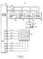
- FIGS. 2 and 3 are block diagrams for showing the second embodiment of the present invention.
- a key input signal input from the keyboard 30 is supplied from the keyboard interface 29 to the CPU of the control section 22 through the specific bus 32.
- a key matrix provided in the keyboard 43 which serves as a PIN input section for inputting PIN information, uses a specific input/output port section 42A provided in advance in a CPU constituting a control section 42.
- the input/output port section 42A comprises four input ports P00 to P03 and four output ports P04 to P07.
- the input ports P00 to P03 are respectively connected to row lines x1 to x4 constituting an input port section 43A for use in inputting PIN or the like.
- the output ports P04 to P07 are respectively connected to column lines y1 to y4 constituting an output port section 43B. Number keys "1", “2", “3” ...
- all key sections respectively corresponding to the keys are normal open type of switches.
- a desired key When a desired key is pushed, its key section enters a closed state, connecting an associated one of the row lines x1 to x4 and an associated one of the column lines y1 to y4.
- the CPU of the control section 42 scans the input ports P00 to P03 and the output ports P04 to P07, detecting which one of the keys is pushed.
- the pushed key can be specified by detecting one of the input ports P00 to P03 which is set at “0". For example, it is detected that the "1" key is pushed, in the case where "0" is output to the output port P04, "1" is output to the output ports P05 to P07, and it is detected that only the input port P00 is set at "0", and the other input ports, i.e., the input ports P01 to P03 are set at "1".
- the keyboard interface 29 shown in FIG. 1 can be omitted. Furthermore, no specific bus is needed to be provided between the key input section 43 and the CPU of the control section 42, since the key input section comprises a key matrix by using the input/output ports P00 to P07 provided in advance in the CPU of the control section 42. By virtue of this feature, it is more difficult to steal the PIN information input by use of the keys than in the first embodiment.
- the above explanations refer to the structures designed to prevent PIN information from being stolen when the PIN information is transmitted from the keyboard to the CPU. Therefore, the following explanation will be given of how the PIN information is prevented from being stolen when the PIN collation command is transmitted from the CPU to the IC card 31, i.e., it passes through the system data bus 24.
- IC card PIN collation instruction information i.e., a PIN collation command, which is produced in such a manner as to include the PIN information, is transmitted through the system data bus 24.
- the PIN collation command is received by the IC card interface 28, and then supplied to the IC card 31 as instruction information, as shown in FIG. 4A.
- the IC card 31 fetches the PIN information from the instruction information, and checks whether or not the PIN information is identical to the PIN information registered in advance in the IC card 31.
- the IC card 31, as shown in FIG. 4A sends answer information representing a result of checking to the IC card interface 28, and then the answer information is sent to the CPU of the control section 22 through the system data bus 24.
- FIG. 4B shows an example of the structure of instruction information produced as a PIN collation command.
- the instruction information comprises a PIN collation instruction code 51, length information 52, a PIN information portion 53, and an information confirmation code 54, which are arranged in that order.
- the length information 52 is information representing the information amount of the entire PIN information portion 53 in the number of bytes. Therefore, when receiving the instruction information, the IC card 31 fetches the PIN information portion 53 from the instruction information by referring to the length information 52, and collates the PIN information portion 53 with the PIN information registered in advance in the IC card 31.
- the answer information sent from the IC card 31 has a structure shown in FIG. 4C, and comprises a PIN collation answer code 55, length information 56, an instruction execution result code 57, and information confirmation code 58, which are arranged in that order.
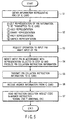
- the IC card 31 to be processed is inserted into the IC card interface 28, and a reset signal necessary for the operation of the IC card 31 is supplied thereto, thereby to obtain an initial answer-to-reset signal from the IC card 31. Then, the operation is shifted to step S1 shown in FIG. 5, and information, e.g., a program version is obtained as information representing the kind of the IC card 31.
- the program version is contained in the IC card 31, and means a program version of a ROM 31A storing an operation program of the IC card 31.
- the CPU checks the program version of the IC card 31 on the basis of the initial answer-to-reset signal, and regards the program version as information representing the kind of the IC card 31.
- the CPU of the control section 22 has a number of information indicating representations one of which is to be applied to the PIN information portion of the PIN collation command, and is selected in accordance with, e.g., the contents of the program version of the IC card 31.
- one of the representations is selected as a representation of PIN information to be sent to the IC card 31 in accordance with version information.
- an ASCII representation As the above representations, an ASCII representation, a binary representation, a pack representation, and an unpack representation are provided. One of those representations is selected in accordance with the program version.
- a display section 25 displays, e.g., characters which requests the operator to input his or her PIN.
- the PIN information obtained from the keyboard interface 29 via the specific bus 32 is modified in accordance with the selected representation, thereby producing instruction information as a PIN collation command to be transmitted to the IC card 31.
- step S5 the produced instruction information is sent from the CPU of the control section 22 to the IC card 31 through the system data bus 24, and is subjected to PIN collation in the IC card 31.
- step S6 information representing a result of collation is sent as answer information from the IC card 31 to the CPU of the control section 22.
- step S7 the CPU checks an instruction execution result code in the answer information, and then, for example, information indicating that the operation is normally ended (normal end) or it is abnormally ended (abnormal end) is displayed on a display section 25 based on a result of checking.
- FIGS. 6A, 6B and 6C show examples of the structures of PIN collation commands which use the ASCII representation, the binary representation, and the pack representation, respectively.
- FIG. 6A shows a PIN collation command produced according to the ASCII representation.
- the PIN collation command contains information of four figures as PIN information, which are obtained, for example from the "1" key, the "2" key, the “3” key and the "4" key of the keyboard 30, respectively. Therefore, a length information portion 62 is represented by length information of 1 byte "04h”.
- PIN information portions 63, 64, 65 and 66 are respectively represented by information of 1 byte "31h”, “32h”, “33h” and “34h” of the ASCII representation. The "h” indicates that the data is hexadecimally represented.
- the length information of a length information portion 72 is "04".
- PIN information portions 73, 74, 75 and 76 are respectively represented by "01h”, "02h”, “03h” and "04" of hexadecimal binary representation.
- the length information of a length information portion 82 is "02h” which is half that of each of the above length information portions 62 and 72.
- PIN information portions 83 and 84 are represented by “12h” and “34h” of the pack representation, respectively, which are obtained by packing "1” and “2” and packing "3” and "4".
- a PIN collation command is produced in accordance with the representation selected in step S2 shown in FIG. 5, and PIN collation processing is executed in the same manner as in the previously inserted IC card.
- FIGS. 5, 6A, 6B and 6C refer to the case where a desired representation is selected as a representation of PIN information from among the ASCII representation, the binary representation, the pack representation, and the unpack representation.
- the order may be changed in which PIN information portions of PIN information produced in accordance with the selected representation are arranged.
- the PIN information is more reliably prevented from being stolen when being sent through the system data bus 24.
- FIGS. 7A to 7F show examples of various modifications of the structure of the PIN collation command.
- FIG. 7A shows a PIN collation command obtained by selecting the forward structure after the ASCII representation is selected as in the PIN collation command shown in FIG. 6A. Therefore, the PIN collation command shown in FIG. 7A is the same as that shown in FIG. 6A in structure.
- FIG. 7B shows a PIN collation command obtained by selecting the reverse structure after the binary representation is selected.
- PIN information portions 63, 64, 65 and 66 are represented by "04h”, “03h”, “02h” and "01h”, respectively.
- FIGS. 7C to 7F respectively show four PIN collation command pieces each obtained by selecting the 1 byte structure, which are necessary for transmission of PIN information of 4 bytes of ASCII representation.
- FIG. 7C shows the structure of the first PIN collation command piece indicating the first one of four figures constituting PIN.
- the first PIN collation command piece consists of a PIN collation instruction code 61, length information 62 represented by "01h”, a PIN information portion 63 represented by "31h” which is the first one of 4 bytes of the PIN information, and an information confirmation code 67.
- the second PIN collation command piece as shown in FIG. 7D, has a PIN information portion 64 which is the second information portion of the command piece from left, and which is represented by "32h” which is the second one of the 4 bytes of the PIN information.
- the third PIN collation command piece as shown FIG.
- the fourth PIN collation command piece has a PIN information portion 66 which is the fourth information portion of the command piece from left, and which is represented by "34h” which is the fourth one of the 4 bytes of the PIN information.
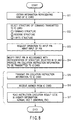
- FIG. 8 is a flowchart of the operation of the IC card processing apparatus which includes a step of selecting the structure of a PIN collation command in the above manner, and illustrates steps which are carried out after reception of an initial answer-to-reset signal from the IC card 31 as in the flowchart of FIG. 5.
- step S11 which is the first step
- information of a program version is obtained as information representing the kind of the IC card 31, as shown in FIG. 8.
- the CPU of the control section 22 has information representing structures one of which is to be applied to the PIN information portions of a PIN collation command, and selects one of the structure in step S12 in accordance with the program version.
- the forward structure, the reverse structure, the 1 byte structure, and the like are provided, and one of them is selected as a structure of the PIN information portions.
- step S13 the display section 25 displays characters which request the operator to input his or her PIN.
- step S14 the PIN information obtained from the keyboard interface 29 through the specific bus 32 is modified in accordance with the representation of the selected structure, thereby producing instruction information as a PIN collation command to be sent to the IC card 31.
- step S15 the produced instruction information is sent from the control section 22 to the IC card 31, and its PIN is collated with the PIN registered in the IC card 31.
- step S16 information representing a result of collation is sent to the control section 22 as answer information.
- step S17 the control section 22 checks an instruction execution result code included in the answer information, and then, for example, the display section 25 displays a normal end or an abnormal end.
- the IC card processing apparatus of the present invention has a structure which has the following features and advantages:
- Transaction information such as PIN information which needs to be kept secret is sent from a keyboard to a control section such as a CPU without passing through a system data bus, thus reliably preventing the information from being stolen.
- the structure or representation of PIN information to be processed by an IC card can be selected, as a result of which the PIN information can be kept secret more reliably.
- the information is prevented from being stolen even when a collation command including the secret information is sent to the IC card through the system data bus.
- a larger number of kinds of IC cards can be processed.
Landscapes
- Physics & Mathematics (AREA)
- General Physics & Mathematics (AREA)
- Financial Or Insurance-Related Operations Such As Payment And Settlement (AREA)
- Storage Device Security (AREA)
Applications Claiming Priority (3)
| Application Number | Priority Date | Filing Date | Title |
|---|---|---|---|
| JP24910797A JP3550279B2 (ja) | 1997-09-12 | 1997-09-12 | Icカ−ド処理装置 |
| JP24910797 | 1997-09-12 | ||
| JP249107/97 | 1997-09-12 |
Publications (3)
| Publication Number | Publication Date |
|---|---|
| EP0903703A2 true EP0903703A2 (de) | 1999-03-24 |
| EP0903703A3 EP0903703A3 (de) | 1999-11-17 |
| EP0903703B1 EP0903703B1 (de) | 2004-04-07 |
Family
ID=17188068
Family Applications (1)
| Application Number | Title | Priority Date | Filing Date |
|---|---|---|---|
| EP98116241A Expired - Lifetime EP0903703B1 (de) | 1997-09-12 | 1998-08-27 | Vorrichtung zum Bearbeiten von Chipkarten |
Country Status (3)
| Country | Link |
|---|---|
| EP (1) | EP0903703B1 (de) |
| JP (1) | JP3550279B2 (de) |
| DE (1) | DE69822952T2 (de) |
Cited By (1)
| Publication number | Priority date | Publication date | Assignee | Title |
|---|---|---|---|---|
| EP2128803A4 (de) * | 2007-02-07 | 2012-01-25 | Toshiba Kk | Informationsspeichermedium und mediumverarbeitungssystem |
Family Cites Families (7)
| Publication number | Priority date | Publication date | Assignee | Title |
|---|---|---|---|---|
| US4105156A (en) * | 1976-09-06 | 1978-08-08 | Dethloff Juergen | Identification system safeguarded against misuse |
| EP0284351A1 (de) * | 1987-03-27 | 1988-09-28 | Cardgard Ltd. | Sicherheitsvorrichtung |
| AU626331B2 (en) * | 1988-10-18 | 1992-07-30 | Oki Electric Industry Co. Ltd. | System for collating personal identification number |
| JP2941361B2 (ja) * | 1990-06-07 | 1999-08-25 | 株式会社東芝 | 携帯可能電子装置 |
| US5604803A (en) * | 1994-06-03 | 1997-02-18 | Sun Microsystems, Inc. | Method and apparatus for secure remote authentication in a public network |
| EP0763791A1 (de) * | 1995-09-14 | 1997-03-19 | Hewlett-Packard Company | Rechnertastatureinheit mit einer Chipkartenschnittstelle |
| JPH09259239A (ja) * | 1996-03-25 | 1997-10-03 | Toshiba Corp | Icカード用携帯端末装置 |
-
1997
- 1997-09-12 JP JP24910797A patent/JP3550279B2/ja not_active Expired - Fee Related
-
1998
- 1998-08-27 DE DE1998622952 patent/DE69822952T2/de not_active Expired - Lifetime
- 1998-08-27 EP EP98116241A patent/EP0903703B1/de not_active Expired - Lifetime
Non-Patent Citations (1)
| Title |
|---|
| None |
Cited By (1)
| Publication number | Priority date | Publication date | Assignee | Title |
|---|---|---|---|---|
| EP2128803A4 (de) * | 2007-02-07 | 2012-01-25 | Toshiba Kk | Informationsspeichermedium und mediumverarbeitungssystem |
Also Published As
| Publication number | Publication date |
|---|---|
| EP0903703A3 (de) | 1999-11-17 |
| DE69822952T2 (de) | 2005-03-10 |
| EP0903703B1 (de) | 2004-04-07 |
| JPH1185927A (ja) | 1999-03-30 |
| JP3550279B2 (ja) | 2004-08-04 |
| DE69822952D1 (de) | 2004-05-13 |
Similar Documents
| Publication | Publication Date | Title |
|---|---|---|
| US6957338B1 (en) | Individual authentication system performing authentication in multiple steps | |
| USRE39808E1 (en) | Computer-based network printing system and method | |
| US6578768B1 (en) | Method and device for selecting a reconfigurable communications protocol between and IC card and a terminal | |
| CA1266326A (en) | Ic card system | |
| EP0838789B1 (de) | Tragbares Chipkartenendgerät und Verfahren zum Überprüfen von Passwörtern | |
| EP0981805B1 (de) | Chipkarte mit datenumsetzer | |
| EP0375386B1 (de) | Tragbare elektronische Vorrichtung und Verfahren zum Kollationieren ihrer geheimen Informationen | |
| US20010016895A1 (en) | Removable memory device for portable terminal device | |
| US4935608A (en) | Card authorization terminal system in which one terminal transmits data to a designated other terminal | |
| WO1999001960A2 (en) | Smart card control of terminal and network resources | |
| US5414753A (en) | Number assignment module setting system for portable telephone set | |
| EP1292870B1 (de) | Informationsdienstgerät | |
| EP0338568A2 (de) | Kartentransaktion-Verarbeitungsvorrichtung | |
| EP1062619B1 (de) | Vorrichtung und verfahren zur auswahl eines rekonfigurierbaren übertragungsprotokolls zwischen einer chipkarte und einem endgerät | |
| EP0903703B1 (de) | Vorrichtung zum Bearbeiten von Chipkarten | |
| US5530893A (en) | System for selectively communicating information between processor and built-in keyboard and external input means | |
| JP2000250860A (ja) | 端末装置のアクセス制限システム | |
| US5719382A (en) | Display peripheral incorporating a wedge interface | |
| EP1981004A1 (de) | Modulares Zahlungsendgerät | |
| US8239324B2 (en) | Mobile terminal | |
| US6168078B1 (en) | Card reader | |
| JP3138691B2 (ja) | Etc用車載器 | |
| EP0488720B1 (de) | Tragbares elektronisches Gerät und Verfahren zur Datenverarbeitung dafür | |
| WO2000042794A1 (en) | Apparatus and method relating to authorisation control | |
| JPH07168788A (ja) | カード使用方法 |
Legal Events
| Date | Code | Title | Description |
|---|---|---|---|
| PUAI | Public reference made under article 153(3) epc to a published international application that has entered the european phase |
Free format text: ORIGINAL CODE: 0009012 |
|
| 17P | Request for examination filed |
Effective date: 19980827 |
|
| AK | Designated contracting states |
Kind code of ref document: A2 Designated state(s): DE FR GB |
|
| AX | Request for extension of the european patent |
Free format text: AL;LT;LV;MK;RO;SI |
|
| PUAL | Search report despatched |
Free format text: ORIGINAL CODE: 0009013 |
|
| AK | Designated contracting states |
Kind code of ref document: A3 Designated state(s): AT BE CH CY DE DK ES FI FR GB GR IE IT LI LU MC NL PT SE |
|
| AX | Request for extension of the european patent |
Free format text: AL;LT;LV;MK;RO;SI |
|
| AKX | Designation fees paid |
Free format text: DE FR GB |
|
| 17Q | First examination report despatched |
Effective date: 20010612 |
|
| GRAP | Despatch of communication of intention to grant a patent |
Free format text: ORIGINAL CODE: EPIDOSNIGR1 |
|
| GRAS | Grant fee paid |
Free format text: ORIGINAL CODE: EPIDOSNIGR3 |
|
| GRAA | (expected) grant |
Free format text: ORIGINAL CODE: 0009210 |
|
| AK | Designated contracting states |
Kind code of ref document: B1 Designated state(s): DE FR GB |
|
| REG | Reference to a national code |
Ref country code: GB Ref legal event code: FG4D |
|
| REF | Corresponds to: |
Ref document number: 69822952 Country of ref document: DE Date of ref document: 20040513 Kind code of ref document: P |
|
| ET | Fr: translation filed | ||
| PLBE | No opposition filed within time limit |
Free format text: ORIGINAL CODE: 0009261 |
|
| STAA | Information on the status of an ep patent application or granted ep patent |
Free format text: STATUS: NO OPPOSITION FILED WITHIN TIME LIMIT |
|
| 26N | No opposition filed |
Effective date: 20050110 |
|
| PGFP | Annual fee paid to national office [announced via postgrant information from national office to epo] |
Ref country code: DE Payment date: 20140821 Year of fee payment: 17 |
|
| PGFP | Annual fee paid to national office [announced via postgrant information from national office to epo] |
Ref country code: FR Payment date: 20140808 Year of fee payment: 17 Ref country code: GB Payment date: 20140827 Year of fee payment: 17 |
|
| REG | Reference to a national code |
Ref country code: DE Ref legal event code: R119 Ref document number: 69822952 Country of ref document: DE |
|
| GBPC | Gb: european patent ceased through non-payment of renewal fee |
Effective date: 20150827 |
|
| REG | Reference to a national code |
Ref country code: FR Ref legal event code: ST Effective date: 20160429 |
|
| PG25 | Lapsed in a contracting state [announced via postgrant information from national office to epo] |
Ref country code: DE Free format text: LAPSE BECAUSE OF NON-PAYMENT OF DUE FEES Effective date: 20160301 Ref country code: GB Free format text: LAPSE BECAUSE OF NON-PAYMENT OF DUE FEES Effective date: 20150827 |
|
| PG25 | Lapsed in a contracting state [announced via postgrant information from national office to epo] |
Ref country code: FR Free format text: LAPSE BECAUSE OF NON-PAYMENT OF DUE FEES Effective date: 20150831 |