EP0903747A2 - Méthode et appareil de commande à vitesse élevée de ligne de mot occupant une petite surface supplémentaire - Google Patents
Méthode et appareil de commande à vitesse élevée de ligne de mot occupant une petite surface supplémentaire Download PDFInfo
- Publication number
- EP0903747A2 EP0903747A2 EP98112432A EP98112432A EP0903747A2 EP 0903747 A2 EP0903747 A2 EP 0903747A2 EP 98112432 A EP98112432 A EP 98112432A EP 98112432 A EP98112432 A EP 98112432A EP 0903747 A2 EP0903747 A2 EP 0903747A2
- Authority
- EP
- European Patent Office
- Prior art keywords
- wordline
- transition
- recited
- wordlines
- logic level
- Prior art date
- Legal status (The legal status is an assumption and is not a legal conclusion. Google has not performed a legal analysis and makes no representation as to the accuracy of the status listed.)
- Withdrawn
Links
Images


Classifications
-
- G—PHYSICS
- G11—INFORMATION STORAGE
- G11C—STATIC STORES
- G11C7/00—Arrangements for writing information into, or reading information out from, a digital store
-
- G—PHYSICS
- G11—INFORMATION STORAGE
- G11C—STATIC STORES
- G11C8/00—Arrangements for selecting an address in a digital store
- G11C8/08—Word line control circuits, e.g. drivers, boosters, pull-up circuits, pull-down circuits, precharging circuits, for word lines
-
- G—PHYSICS
- G11—INFORMATION STORAGE
- G11C—STATIC STORES
- G11C11/00—Digital stores characterised by the use of particular electric or magnetic storage elements; Storage elements therefor
- G11C11/21—Digital stores characterised by the use of particular electric or magnetic storage elements; Storage elements therefor using electric elements
- G11C11/34—Digital stores characterised by the use of particular electric or magnetic storage elements; Storage elements therefor using electric elements using semiconductor devices
- G11C11/40—Digital stores characterised by the use of particular electric or magnetic storage elements; Storage elements therefor using electric elements using semiconductor devices using transistors
- G11C11/401—Digital stores characterised by the use of particular electric or magnetic storage elements; Storage elements therefor using electric elements using semiconductor devices using transistors forming cells needing refreshing or charge regeneration, i.e. dynamic cells
- G11C11/4063—Auxiliary circuits, e.g. for addressing, decoding, driving, writing, sensing or timing
- G11C11/407—Auxiliary circuits, e.g. for addressing, decoding, driving, writing, sensing or timing for memory cells of the field-effect type
- G11C11/408—Address circuits
- G11C11/4085—Word line control circuits, e.g. word line drivers, - boosters, - pull-up, - pull-down, - precharge
Definitions
- the present invention relates to semiconductor memory devices. More particularly, the invention relates to improved wordline driving for semiconductor memory devices.
- a memory array is configured with wordlines and bitlines running in an orthogonal manner.
- the memory array includes a larger number of memory cells placed at the intersection of each wordline and bitline.
- Each memory cell is formed from a single transistor and a capacitive storage element.
- FIG. 1 is a schematic diagram of a basic DRAM memory cell 100 for a DRAM integrated circuit.
- the basic DRAM memory cell 100 includes a cell transistor 102 and a capacitive storage element 104.
- the cell transistor 102 couples to a wordline (WL) 106 and a bitline (BL) 108 of the DRAM integrated circuit.
- the gate of the cell transistor 102 is connected to the wordline (WL) 106.
- the transistor 102 also has a first channel terminal and a second channel terminal.
- the first channel terminal of the cell transistor 102 is connected to the bitline (BL) 108 and the second channel terminal of the cell transistor 102 is connected to a first side of the capacitive storage element 104.
- the second side of the capacitive storage element 104 is connected to a supply voltage V C .
- the wordlines for the memory cells of a DRAM integrated circuit are driven from one side of the memory array by wordline drivers.
- wordline drivers typically, the number of the memory cells coupled to a given wordline is continually increasing.
- the wordlines in a DRAM integrated circuit are heavily loaded by parasitic capacitance.
- the parasitic capacitance on the wordlines makes it difficult to transition the wordlines at high speed and thus operate the DRAM integrated circuit at high speed.
- FIG. 2 is a block diagram of a conventional DRAM integrated circuit 200.
- the DRAM integrated circuit 200 includes a memory array 202, a row decoder 204 and a column decoder 206.
- the memory array 202 includes an array of memory cells such as depicted in FIG. 1.
- the memory cells are addressed individually by a row and column combination.
- the row is selected by the row decoder 204 in accordance with a row address 208.
- the column is selected by the column decoder 206 in accordance with a column address 210.
- the data to be stored at the addressed memory cell is either provided to the column decoder 206 by a data bus 212 or output by the column decoder 206 over the data bus 212.
- the row decoder 204 operates to select a wordline then causes the selected wordline to be activated.
- the parasitic capacitance makes it difficult to rapidly transition the selected wordline.
- One approach to driving the wordlines at faster speeds operates to increase the driving ability of the wordline drivers provided at one end of the wordlines.
- the size of the wordline drivers are increased to provide the increase in driving ability.
- This approach is generally effective but the die area penalty is rather severe for the improvement in performance provided.
- Another approach would be to provide a second set of row decoder circuits, drivers and associated wiring so that the wordlines could be driven from both ends. Again, the die area penalty for such a design renders it impractical to implement in most semiconductor memory designs.
- the invention relates to improved techniques for driving wordlines of a semiconductor memory device.
- a wordline is driven by a wordline driver at a first end and then provided with a small amount of additional circuitry at the other end of the wordline.
- the additional circuitry senses that the wordline is beginning to transition to an active state, the additional circuitry operates to assist or accelerate the transition of the wordline to the active state.
- the invention operates to rapidly transition wordlines to an active state while using only minimal amounts of die area.
- the invention is particularly well suited for dynamic random access memories.
- the invention can be implemented in numerous ways, including as an apparatus, a circuit, and a method. Several embodiments of the invention are discussed below.
- an embodiment of the invention includes: a memory array having an array of memory cells, a plurality of bitlines, and a plurality of wordlines: an address decoder for receiving an address for a data request and selecting one of the plurality of wordlines and one of a plurality of bitlines, the selected wordline having a first side and a second side; a line driver for driving the selected wordline at the first side; and a line transition accelerator circuit for detecting an initial part of a transition in a first direction on the selected wordline and then accelerating a remaining part of the transition on the selected wordline in the first direction from the second side.
- the line transition accelerator circuit includes: a level sense circuit coupled to the selected wordline, and a switch circuit coupled to the selected wordline.
- the level sense circuit monitors a voltage level on the selected wordline to produce a voltage level signal.
- the switch circuit operates to pull the selected wordline towards a predetermined supply potential based on the voltage level signal.
- an embodiment of the invention includes: a memory array having an array of memory cells, a plurality of bitlines, and a plurality of wordlines; a wordline driver for each of the wordlines; monitoring means for determining that at least one of the wordlines is beginning to transition from an inactive state to an active state; and assistance means for assisting the wordline driver associated with the one of the wordlines that is beginning to transition, the assistance means operates to assist in driving the transition of the one of the wordlines that is beginning to transition from the inactive state to the active state.
- an embodiment of the invention includes the operations of: receiving a control signal having one of an enable stale and a disable state; monitoring a wordline; determining whether the monitored wordline is beginning to transition from a first logic level to a second logic level: and pulling the monitored wordline to the second level when both the control signal has the enable state and the determining determines that the monitored wordline has begun to transition from the first logic level to the second logic level.
- wordline switching e.g., activation
- wordlines are able to handle more memory cells in a memory array (i.e., denser memory arrays) because of the more robust switching provided by the invention.
- the invention relates to improved techniques for driving wordlines of a semiconductor memory integrated circuit (IC).
- a memory IC includes a random access memory (RAM), a dynamic random access memory (DRAM), a synchronous DRAM (SDRAM) and merged DRAM-logic (embedded DRAM).
- RAM random access memory
- DRAM dynamic random access memory
- SDRAM synchronous DRAM
- ASIC application specific integrated circuit
- a plurality of ICs are formed on the wafer in parallel. After processing is finish, the wafer is diced to separate the ICs to individual chips. The chips are then packaged, resulting in a final product that is used in: for example, consumer products such as computer systems, cellular phones, personal digital assistants (PDAs), and other electronic products.
- PDAs personal digital assistants
- a wordline is driven by a wordline driver at a first end and then provided with a small amount of additional circuitry at the other end of the wordline.
- the additional circuitry senses that the wordline is beginning to transition to an active state, the additional circuitry operates to assist or accelerate the transition of the wordline to the active state. Accordingly, the invention operates to rapidly transition wordlines to an active state while using only minimal amounts of die area.
- the invention is particularly well suited for dynamic random access memories.
- FIG. 3 is a block diagram of a semiconductor memory circuit 300 according to an embodiment of the invention.
- the semiconductor memory is, for example, a DRAM circuit.
- the DRAM semiconductor memory circuit 300 includes a memory array 302 that includes a plurality of memory cells arranged in an array configuration. The individual memory cells can be selected through a combination of a selected wordline and a selected bitline.
- a row decoder 304 receives a row address signal 306 and selects one of a plurality of wordlines (WL 1 - WL n ) 308.
- the column decoder 310 receives a column address signal 312 illustrated in FIG. 3 and selects one of a plurality of bitlines (BL 1 - Bl m ) 308. Additionally, data is supplied to or read from a selected memory cell of the memory array 302 by a data bus 316 coupled to the column decoder 310.
- the DRAM semiconductor memory circuit 300 also includes latch circuitry 318.
- the latch circuitry 318 couples to the wordlines (WL 1 - WL n ) 308 of the memory array 302.
- the latch circuitry 314 also receives a control signal 320 that operates to control when the latch circuitry 314 is permitted to perform a latching operation.
- the latching operation performed by the latch circuitry 314 is individually on each of the wordlines (WL 1 - WL n ) 308 and operates to accelerate the transition of the selected wordline (WL) so that the DRAM semiconductor memory circuit 300 can operate at faster speeds. Only one of the wordlines (WL 1 - WL n ) 308 is normally transitioning at any point in time.
- latch circuitry 314 illustrated in FIG. 3 is shown as being separate from the memory array 302, the latch circuitry 314 is preferably integrated within the memory array 302.
- One advantage of providing the latch circuitry 314 integral to the memory array 302 is that the connections of the latch circuitry 314 to the wordlines is facilitated.
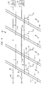
- FIG. 4 illustrates a memory array 400 according to an embodiment of the invention.
- the memory array 400 includes wordlines, bitlines and memory cells of a memory array as well as latch circuits for accelerated operation. More specifically, the memory array 400 illustrated in FIG. 4 shows a portion of a memory array of a semiconductor memory device. The portion illustrated in FIG. 4 contains two wordlines WL x and WL y and various bitlines.
- the memory array 400 includes metal wordlines 402 and 404.
- the metal wordline 402 is driven by a wordline driver 406 and coupled to wordline WL x
- the metal wordline 404 is driven by a wordline driver 408 and coupled to the wordline WL y .
- the metal wordlines are metal lines that are sometimes stitched frequently to poly-silicon segments that run in parallel and underneath the metal wordlines.
- the metal wordline 402 has poly-silicon segments 410 and 412 runing in parallel underneath the metal wordline.
- the metal wordline 404 has poly-silicon segments 414 and 416 running in parallel underneath the metal wordline 414.
- a single metal wordline might have eight (8) poly-silicon segments.
- the memory array 400 also includes metal bitline pairs that intersect the metal wordlines. Such a configuration is referred to as a folded-bitline architecture. Other bitline configurations, such as open or open-folder, are also used. Illustratively, the bitlines are orthogonal to the metal wordlines. Intersections of the bitlines to the wordlines at angles other than 90° are also useful. Memory cells, such as memory cells 418 and 420, are provided at the intersection of each meal wordline and metal bitline. A first bitline 422-1 of a first pair of metal bitlines 422 couples to a first channel terminal of a cell transistor 424. A second channel terminal of the cell transistor 424 is coupled to a first side of a capacitive storage element 426.
- a second side of the capacitive storage element 426 is coupled to supply voltage (V ss ).
- the gate of the cell transistor 424 couples to the associated poly-silicon segment 414.
- a like storage cell is provided and coupled to the first bitline 422-1 of the bitline pair 422 in a similar manner.
- a second bitline 428-2 of the bitline pair 428 couples to a first channel terminal of a cell transistor 430.
- the second channel terminal of the cell transistor 430 is coupled to a first side of a capacitive storage element 432.
- a second side of the capacitive storage element 432 is connected to supply voltage (V ss ).
- the gate of the cell transistor 430 couples to the associated poly-silicon segment 414.
- a like storage cell is provided and coupled to the second bitline 428-2 of the bitline pair 428.
- the memory array 400 includes other metal bitline pairs, such as bitline pairs 438 and 440.
- bitline pairs 438 and 440 similarly include memory cells 434 and 436, respectively, for each wordline.
- each of the wordlines within the memory array 400 include a wordline latch circuit.
- the metal wordline 402 is coupled to a wordline latch circuit 442, and the metal wordline 404 is coupled to a wordline latch circuit 442.
- the wordline driver 406 is coupled to a first end of the associated metal wordline 402 and the wordline latch circuit 442 is coupled to a second end of the associated metal wordline 402.
- the wordline driver 408 is coupled to a first end of the associated metal wordline 404 and the wordline latch circuit 444 is coupled to a second end of the associated metal wordline 404.
- the wordline latch circuits 442 and 444 represent individual circuit portions of the latch circuitry 314 illustrated in FIG. 3. The structure and operation of the wordline latch circuits 442 and 444 are described in detail below with respect to FIGs. 5 and 6.
- FIG. 5 is a block diagram of a wordline latch circuit 500 according to an embodiment of the invention.
- the wordline latch circuit 500 receives a wordline (WL) 502 at an input to a level sense device 504.
- the level sense device 504 operates to monitor a signal level (e.g., voltage) on the wordline (WL) 502. In this embodiment, the signal level is assumed to be a voltage level.
- a voltage level signal 506 informs a control circuit 508 that the wordline (WL) 502 has begun to transition from a first logic state (e.g., 0 volts) to a second logic level (e.g., V DD ).
- the control circuit 508 receives the voltage level signal 506 and also receives a control signal 510.
- a control signal 510 is provided to the wordline latch circuit 500 to enable the wordline latch circuit 500.
- the wordline latch circuit 500 is enabled, the wordline latch circuit 500 is permitted to perform its latching operation.
- the wordline latch circuit 500 is disabled, then the wordline latch circuit 500 is not able to perform its latching operation.
- the semiconductor memory device is not negatively impacted by the presence of the wordline latch circuit 500.
- control circuit 508 determines that the voltage level signal 506 indicates that the wordline (WL) 502 has begun to transition and that the control signal 510 has enabled (authorized) its latching operation, then the control circuit 508 produces a control signal 512 that causes a switch device 514 to electrically couple the wordline (WL) 502 to a supply potential (V SUPPLY ).
- V SUPPLY supply potential
- the switch device 514 is activated to electrically couple the wordline (WL) 502 to the supply potential (V SUPPLY )
- the transitioning of the wordline (WL) 502 that has begun and detected by the level sense device 504 is assisted so that the transition of the wordline (WL) 502 can complete faster than otherwise possible if the semiconductor memory device did not include the wordline latch circuit 500.
- the switch device 514 when the switch device 514 is activated to electrically couple the wordline (WL) 502 to the supply potential (V SUPPLY ), the wordline (WL) 502 is "pulled up” from its existing voltage level to the supply potential (V SUPPLY ).
- the control circuit 508 determines that either the control signal 510 is disabling the wordline latch circuit 500 (i.e., does not authorize its latching operation) or that the voltage level signal 506 does not indicate that the wordline (WL) 502 has begun to transition, the control signal 512 causes the switch device 514 to isolate the supply potential (V SUPPLY ) from the wordline (WL) 502.
- FIG. 6 is a schematic diagram of a latch circuit 600 according to an embodiment of the invention.
- the latch circuit 600 is one suitable implementation of the wordline latch circuits 442 and 444 illustrated in FIG. 4.
- the latch circuit 600 is also a suitable implementation of the latch circuit 500 illustrated in FIG. 5.
- the latch circuit 600 couples to a wordline (WL) 602 and receives a control signal (CS) 604.
- the wordline (WL) 602 couples to a gate of a first transistor 606.
- the first transistor 606 is preferably a low threshold device.
- the control signal (CS) 604 is received at a first node 608 of the latch circuit 600.
- the latch circuit 600 also includes a second transistor 610 and a third transistor 612. The gate terminals of both the second transistor 610 and the third transistor 612 are coupled to the first node 608.
- a first channel terminal of the second transistor 610 is connected to a first supply potential (V S ), and a second channel terminal of the second transistor 610 is connected to a second node 614 of the latch circuit 600.
- a first channel terminal of the third transistor 612 is connected to the second node 614, and a second channel terminal of the third transistor 612 is connected to a first channel terminal of the first transistor 606.
- the second channel terminal for the first transistor 606 is connected to a second supply potential (GND).
- the latch circuit 600 also includes a fourth transistor 616.
- a gate terminal for the fourth transistor 616 is connected to the second node 614.
- a first channel terminal for the fourth transistor 616 is connected to the first supply potential (V S ), and a second channel terminal is connected to the wordline (WL) 602.
- the first transistor 606 and the third transistor 612 are n-type field-effect transistors, and the second transistor 610 and the fourth transistor 616 are p-type field-effect transistors.
- the latch circuit 600 is also designed to "pull-up" the wordline (WL) 602 when the wordline (WL) 602 is being activated (i.e., when the wordline (WL) 602 is transitioning to active state). In other words in this embodiment it is assumed that the wordline (WL) 602 is activated at a high logic level and inactive at a low logic level.
- the latch circuit 600 thus operates to "pull-up" the wordline (WL) 602 from the low logic level to the high logic level once it has been determined that the wordline (WL) has begun to transition to the active state.
- the wordline (WL) 602 is able to transition rapidly even in the presence of significant amounts of parasitic capacitance on the wordline (WL) 602.
- the wordline (WL) could be "pulled-down" to a low logic level in a situation in which it was desirable to rapidly transition the wordline (WL) from a high logic level to a low logic level. Such would be the case in a memory array configuration in which the wordline (WL) were active at a low logic level.
- the alternative embodiment would be similar to the latch circuit 600 but modified such that the n-type devices would be replaced by p-type devices and the supply potentials would be reversed.
- the control signal 604 is preferably used to enable the latch circuit 600 just prior to the wordline (WL) being activated. Further, the control signal 604 is then preferably subsequently removed after the latch circuit 600 is no longer required to assist with the transition of the wordline. In other words, the latch circuit 600 should be activated only during wordline rise. It is advantageous that the latch circuitry be disabled as soon as it is no longer needed to assist with the wordline (WL) transition because a capacitive coupling effect with neighboring wordlines could possibly trigger adjacent latch circuits and cause them to erroneously "pull-up" other wordlines since the second nodes 614 are floating in this condition. As an example, the floating of the second node 614 for up to about 7 ns has shown to be tolerable in a 64 megabit DRAM integrated circuit design.
- the threshold voltage for the first transistor 606 should be set such that accidental triggering due to noise is avoided.
- a wordline might have about 200 mV (millivolts) of noise present, so the voltage threshold used by the latch circuit might be set at a value of 400 mV or more.
- the transistor 606 would preferably be a low threshold device with its threshold voltage set at a suitable value, such as 400 mV.
- the advantages of the invention are faster wordline switching with only a minimal amount of additional circuitry and die area requirements. In comparison, to provide circuitry for a complete second row decoder, the are savings is significant, for example, perhaps as much as 90% less die area.
- Another advantage of the invention is that wordlines are able to handle more memory cells in a memory array (i.e., denser memory arrays) because of the more robust switching provided by the invention.
Landscapes
- Engineering & Computer Science (AREA)
- Microelectronics & Electronic Packaging (AREA)
- Computer Hardware Design (AREA)
- Dram (AREA)
- Static Random-Access Memory (AREA)
Applications Claiming Priority (2)
| Application Number | Priority Date | Filing Date | Title |
|---|---|---|---|
| US932925 | 1997-09-19 | ||
| US08/932,925 US6034913A (en) | 1997-09-19 | 1997-09-19 | Apparatus and method for high-speed wordline driving with low area overhead |
Publications (2)
| Publication Number | Publication Date |
|---|---|
| EP0903747A2 true EP0903747A2 (fr) | 1999-03-24 |
| EP0903747A3 EP0903747A3 (fr) | 1999-07-14 |
Family
ID=25463162
Family Applications (1)
| Application Number | Title | Priority Date | Filing Date |
|---|---|---|---|
| EP98112432A Withdrawn EP0903747A3 (fr) | 1997-09-19 | 1998-07-04 | Méthode et appareil de commande à vitesse élevée de ligne de mot occupant une petite surface supplémentaire |
Country Status (6)
| Country | Link |
|---|---|
| US (1) | US6034913A (fr) |
| EP (1) | EP0903747A3 (fr) |
| JP (1) | JPH11149769A (fr) |
| KR (1) | KR19990029320A (fr) |
| CN (1) | CN1150555C (fr) |
| TW (1) | TW394945B (fr) |
Cited By (1)
| Publication number | Priority date | Publication date | Assignee | Title |
|---|---|---|---|---|
| WO2008150844A1 (fr) * | 2007-05-31 | 2008-12-11 | Marvell World Trade Ltd. | Structure de mémoire avec tampons de ligne de mot |
Families Citing this family (14)
| Publication number | Priority date | Publication date | Assignee | Title |
|---|---|---|---|---|
| JP4191827B2 (ja) * | 1998-10-14 | 2008-12-03 | 株式会社東芝 | 半導体記憶装置 |
| DE19952258A1 (de) * | 1999-10-29 | 2001-05-10 | Infineon Technologies Ag | Integrierter Speicher |
| US7570523B2 (en) * | 2006-07-31 | 2009-08-04 | Sandisk 3D Llc | Method for using two data busses for memory array block selection |
| US8279704B2 (en) * | 2006-07-31 | 2012-10-02 | Sandisk 3D Llc | Decoder circuitry providing forward and reverse modes of memory array operation and method for biasing same |
| US7499366B2 (en) | 2006-07-31 | 2009-03-03 | Sandisk 3D Llc | Method for using dual data-dependent busses for coupling read/write circuits to a memory array |
| US7463536B2 (en) * | 2006-07-31 | 2008-12-09 | Sandisk 3D Llc | Memory array incorporating two data busses for memory array block selection |
| JP2008108417A (ja) * | 2006-10-23 | 2008-05-08 | Hynix Semiconductor Inc | 低電力dram及びその駆動方法 |
| US8259509B2 (en) | 2008-08-18 | 2012-09-04 | Elpida Memory, Inc. | Semiconductor memory device and method with auxiliary I/O line assist circuit and functionality |
| JP5431066B2 (ja) * | 2008-08-18 | 2014-03-05 | ピーエスフォー ルクスコ エスエイアールエル | 半導体装置 |
| CN102420007B (zh) * | 2011-11-30 | 2013-08-14 | 中国科学院微电子研究所 | 一种字线偏置电路 |
| CN102592655B (zh) * | 2011-11-30 | 2014-01-29 | 中国科学院微电子研究所 | 自举预充电的快速限幅字线偏置电路 |
| US8675427B2 (en) | 2012-03-07 | 2014-03-18 | International Business Machines Corporation | Implementing RC and coupling delay correction for SRAM |
| WO2021095232A1 (fr) * | 2019-11-15 | 2021-05-20 | キオクシア株式会社 | Système de stockage et tranche |
| US11211113B1 (en) * | 2020-08-18 | 2021-12-28 | Micron Technology, Inc. | Integrated assemblies comprising wordlines having ends selectively shunted to low voltage for speed transitioning |
Family Cites Families (13)
| Publication number | Priority date | Publication date | Assignee | Title |
|---|---|---|---|---|
| JPS55150189A (en) * | 1979-05-10 | 1980-11-21 | Nec Corp | Memory circuit |
| US4291392A (en) * | 1980-02-06 | 1981-09-22 | Mostek Corporation | Timing of active pullup for dynamic semiconductor memory |
| US4397003A (en) * | 1980-06-02 | 1983-08-02 | Mostek Corporation | Dynamic random access memory |
| JPS58169958A (ja) * | 1982-03-31 | 1983-10-06 | Fujitsu Ltd | Misスタテイツク・ランダムアクセスメモリ |
| JPS61237292A (ja) * | 1985-04-15 | 1986-10-22 | Hitachi Micro Comput Eng Ltd | 半導体記憶装置 |
| US4901280A (en) * | 1986-07-11 | 1990-02-13 | Texas Instruments Incorporated | Pull-up circuit for high impedance word lines |
| US5422857A (en) * | 1989-11-21 | 1995-06-06 | Matsushita Electric Industrial Co., Ltd. | Semiconductor memory unit having overlapping addresses |
| KR930002574B1 (ko) * | 1990-03-09 | 1993-04-03 | 금성일렉트론 주식회사 | 워드라인 구동회로 |
| EP0552941B1 (fr) * | 1992-01-21 | 1998-07-08 | STMicroelectronics, Inc. | Amélioration d'une impulsion sur une ligne pour signaux dans des circuits intégrés |
| US5381377A (en) * | 1992-10-14 | 1995-01-10 | Sun Microsystems, Inc. | Word line driver circuit and method |
| KR0119887B1 (ko) * | 1994-06-08 | 1997-10-30 | 김광호 | 반도체 메모리장치의 웨이퍼 번-인 테스트 회로 |
| JPH0936328A (ja) * | 1995-07-14 | 1997-02-07 | Hitachi Ltd | ダイナミック型ram |
| KR0164358B1 (ko) * | 1995-08-31 | 1999-02-18 | 김광호 | 반도체 메모리 장치의 서브워드라인 디코더 |
-
1997
- 1997-09-19 US US08/932,925 patent/US6034913A/en not_active Expired - Lifetime
-
1998
- 1998-07-04 EP EP98112432A patent/EP0903747A3/fr not_active Withdrawn
- 1998-07-30 TW TW087112534A patent/TW394945B/zh not_active IP Right Cessation
- 1998-08-19 KR KR1019980033573A patent/KR19990029320A/ko not_active Ceased
- 1998-08-20 CN CNB981184871A patent/CN1150555C/zh not_active Expired - Fee Related
- 1998-09-18 JP JP10264932A patent/JPH11149769A/ja not_active Withdrawn
Cited By (2)
| Publication number | Priority date | Publication date | Assignee | Title |
|---|---|---|---|---|
| WO2008150844A1 (fr) * | 2007-05-31 | 2008-12-11 | Marvell World Trade Ltd. | Structure de mémoire avec tampons de ligne de mot |
| KR101446726B1 (ko) * | 2007-05-31 | 2014-10-06 | 마벨 월드 트레이드 리미티드 | 워드 라인 버퍼를 갖는 메모리 구조 |
Also Published As
| Publication number | Publication date |
|---|---|
| JPH11149769A (ja) | 1999-06-02 |
| US6034913A (en) | 2000-03-07 |
| KR19990029320A (ko) | 1999-04-26 |
| CN1150555C (zh) | 2004-05-19 |
| TW394945B (en) | 2000-06-21 |
| CN1213139A (zh) | 1999-04-07 |
| EP0903747A3 (fr) | 1999-07-14 |
Similar Documents
| Publication | Publication Date | Title |
|---|---|---|
| US6034913A (en) | Apparatus and method for high-speed wordline driving with low area overhead | |
| US5581500A (en) | Memory cell with power supply induced reversed-bias pass transistors for reducing off-leakage current | |
| EP0952588B1 (fr) | Circuit élévateur de tension limitant la tension élévée | |
| US5726941A (en) | Semiconductor integrated circuit | |
| EP0600692B1 (fr) | Circuit de mémoire morte à masse virtuelle | |
| US9640251B2 (en) | Multi-port memory cell | |
| US20080205184A1 (en) | Semiconductor memory device | |
| US5652730A (en) | Semiconductor memory device having hierarchical boosted power-line scheme | |
| US11626159B2 (en) | Computing in-memory device supporting arithmetic operations and method of controlling the same | |
| US5075571A (en) | PMOS wordline boost cricuit for DRAM | |
| US4338678A (en) | Memory device | |
| US20040246799A1 (en) | Memory devices having bit line precharge circuits with off current precharge control and associated bit line precharge methods | |
| US6212094B1 (en) | Low power SRAM memory cell having a single bit line | |
| US4079462A (en) | Refreshing apparatus for MOS dynamic RAMs | |
| JPH06162776A (ja) | 半導体メモリ回路 | |
| US5748556A (en) | Tristatable driver for internal data bus lines | |
| US6667910B2 (en) | Method and apparatus for discharging an array well in a flash memory device | |
| US6542432B2 (en) | Sub word line drive circuit for semiconductor memory device | |
| US5590089A (en) | Address transition detection (ATD) circuit | |
| EP0451000B1 (fr) | Dispositif de mémoire à semi-conducteurs avec fonction de contrÔle perfectionnée pour le bus pour les données | |
| KR20010112597A (ko) | 반도체 메모리 장치 | |
| US20090109777A1 (en) | Sense amplifier power supply circuit | |
| EP0547892A2 (fr) | Circuit intégré avec des lignes de données différentielles auto polarisées | |
| HK1016739A (en) | Apparatus and method for high-speed wordline driving with low area overhead | |
| KR20010055932A (ko) | 서브 워드라인 구동 동작을 안정화시킨 반도체 메모리 소자 |
Legal Events
| Date | Code | Title | Description |
|---|---|---|---|
| PUAI | Public reference made under article 153(3) epc to a published international application that has entered the european phase |
Free format text: ORIGINAL CODE: 0009012 |
|
| AK | Designated contracting states |
Kind code of ref document: A2 Designated state(s): DE FR GB IE IT NL |
|
| AX | Request for extension of the european patent |
Free format text: AL;LT;LV;MK;RO;SI |
|
| PUAL | Search report despatched |
Free format text: ORIGINAL CODE: 0009013 |
|
| AK | Designated contracting states |
Kind code of ref document: A3 Designated state(s): AT BE CH CY DE DK ES FI FR GB GR IE IT LI LU MC NL PT SE |
|
| AX | Request for extension of the european patent |
Free format text: AL;LT;LV;MK;RO;SI |
|
| 17P | Request for examination filed |
Effective date: 19991015 |
|
| AKX | Designation fees paid |
Free format text: DE FR GB IE IT NL |
|
| 17Q | First examination report despatched |
Effective date: 20020530 |
|
| RAP1 | Party data changed (applicant data changed or rights of an application transferred) |
Owner name: INFINEON TECHNOLOGIES AG |
|
| STAA | Information on the status of an ep patent application or granted ep patent |
Free format text: STATUS: THE APPLICATION IS DEEMED TO BE WITHDRAWN |
|
| 18D | Application deemed to be withdrawn |
Effective date: 20040624 |
|
| REG | Reference to a national code |
Ref country code: HK Ref legal event code: WD Ref document number: 1016739 Country of ref document: HK |