EP0903792A3 - Method of manufacturing a plurality of semiconductor bodies - Google Patents
Method of manufacturing a plurality of semiconductor bodies Download PDFInfo
- Publication number
- EP0903792A3 EP0903792A3 EP98117796A EP98117796A EP0903792A3 EP 0903792 A3 EP0903792 A3 EP 0903792A3 EP 98117796 A EP98117796 A EP 98117796A EP 98117796 A EP98117796 A EP 98117796A EP 0903792 A3 EP0903792 A3 EP 0903792A3
- Authority
- EP
- European Patent Office
- Prior art keywords
- hauptfläche
- main surface
- substratwafers
- windows
- exposed
- Prior art date
- Legal status (The legal status is an assumption and is not a legal conclusion. Google has not performed a legal analysis and makes no representation as to the accuracy of the status listed.)
- Granted
Links
- 239000004065 semiconductor Substances 0.000 title abstract 3
- 238000004519 manufacturing process Methods 0.000 title abstract 2
- 235000012431 wafers Nutrition 0.000 abstract 4
- 239000000758 substrate Substances 0.000 abstract 2
- 230000008021 deposition Effects 0.000 abstract 1
- 238000000034 method Methods 0.000 abstract 1
Classifications
-
- H—ELECTRICITY
- H01—ELECTRIC ELEMENTS
- H01S—DEVICES USING THE PROCESS OF LIGHT AMPLIFICATION BY STIMULATED EMISSION OF RADIATION [LASER] TO AMPLIFY OR GENERATE LIGHT; DEVICES USING STIMULATED EMISSION OF ELECTROMAGNETIC RADIATION IN WAVE RANGES OTHER THAN OPTICAL
- H01S5/00—Semiconductor lasers
- H01S5/02—Structural details or components not essential to laser action
- H01S5/0201—Separation of the wafer into individual elements, e.g. by dicing, cleaving, etching or directly during growth
-
- H—ELECTRICITY
- H10—SEMICONDUCTOR DEVICES; ELECTRIC SOLID-STATE DEVICES NOT OTHERWISE PROVIDED FOR
- H10H—INORGANIC LIGHT-EMITTING SEMICONDUCTOR DEVICES HAVING POTENTIAL BARRIERS
- H10H20/00—Individual inorganic light-emitting semiconductor devices having potential barriers, e.g. light-emitting diodes [LED]
- H10H20/01—Manufacture or treatment
- H10H20/011—Manufacture or treatment of bodies, e.g. forming semiconductor layers
- H10H20/013—Manufacture or treatment of bodies, e.g. forming semiconductor layers having light-emitting regions comprising only Group III-V materials
- H10H20/0133—Manufacture or treatment of bodies, e.g. forming semiconductor layers having light-emitting regions comprising only Group III-V materials with a substrate not being Group III-V materials
- H10H20/01335—Manufacture or treatment of bodies, e.g. forming semiconductor layers having light-emitting regions comprising only Group III-V materials with a substrate not being Group III-V materials the light-emitting regions comprising nitride materials
-
- H—ELECTRICITY
- H10—SEMICONDUCTOR DEVICES; ELECTRIC SOLID-STATE DEVICES NOT OTHERWISE PROVIDED FOR
- H10H—INORGANIC LIGHT-EMITTING SEMICONDUCTOR DEVICES HAVING POTENTIAL BARRIERS
- H10H20/00—Individual inorganic light-emitting semiconductor devices having potential barriers, e.g. light-emitting diodes [LED]
- H10H20/01—Manufacture or treatment
- H10H20/011—Manufacture or treatment of bodies, e.g. forming semiconductor layers
- H10H20/013—Manufacture or treatment of bodies, e.g. forming semiconductor layers having light-emitting regions comprising only Group III-V materials
- H10H20/0137—Manufacture or treatment of bodies, e.g. forming semiconductor layers having light-emitting regions comprising only Group III-V materials the light-emitting regions comprising nitride materials
Landscapes
- Physics & Mathematics (AREA)
- Condensed Matter Physics & Semiconductors (AREA)
- General Physics & Mathematics (AREA)
- Electromagnetism (AREA)
- Optics & Photonics (AREA)
- Led Devices (AREA)
- Semiconductor Lasers (AREA)
- Weting (AREA)
- Drying Of Semiconductors (AREA)
- Physical Vapour Deposition (AREA)
Abstract
Verfahren zum Herstellen einer Mehrzahl von Halbleiterkörpern (1) mit folgenden Verfahrensschritten:
- Aufbringen einer Maskenschicht (4) auf eine Hauptfläche (9) eines Substratwafers (19)
- Ausbilden einer Mehrzahl von Fenstern (10) in der Maskenschicht (4), in denen die Hauptfläche (9) des Substratwafers (19) freigelegt ist,
- Abscheiden einer Halbleiterschichtenfolge (18) auf die in den Fenstern (10) freigelegte Hauptfläche (9) und
- Vereinzeln des derart hergestellten Wafers (24).
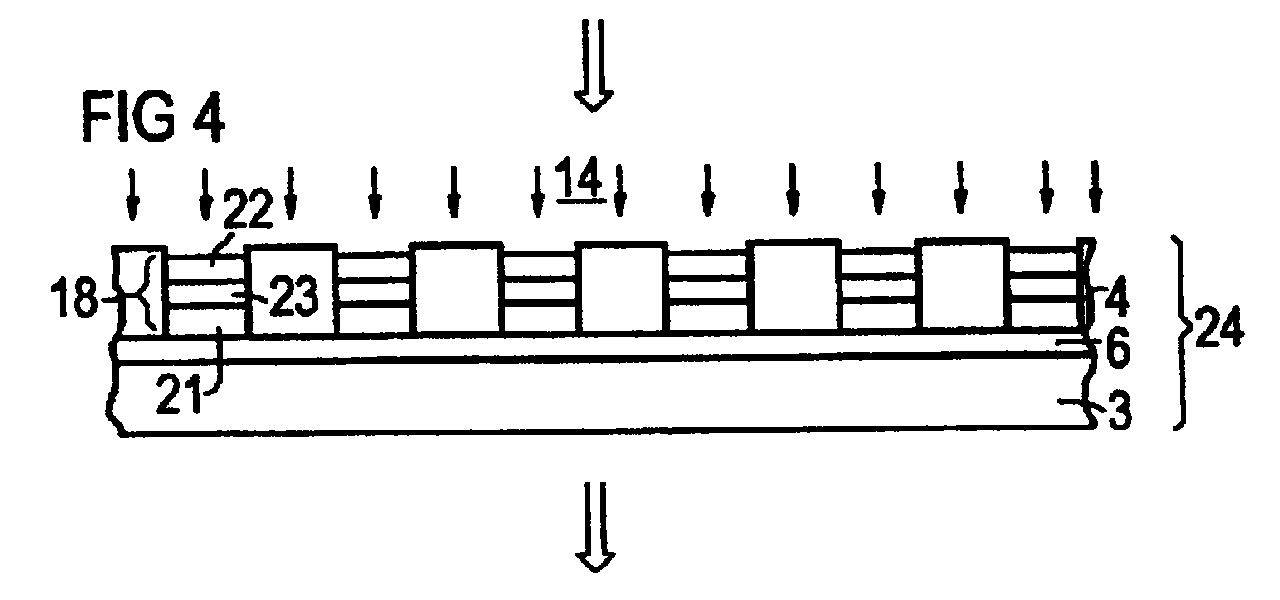
- Applying a mask layer (4) to a main surface (9) of a substrate wafer (19)
- Forming a plurality of windows (10) in the mask layer (4), in which the main surface (9) of the substrate wafer (19) is exposed,
- Deposition of a semiconductor layer sequence (18) on the main surface (9) and exposed in the windows (10)
- Separating the wafer (24) thus produced.
Applications Claiming Priority (4)
| Application Number | Priority Date | Filing Date | Title |
|---|---|---|---|
| DE19741442 | 1997-09-19 | ||
| DE19741442A DE19741442A1 (en) | 1997-09-19 | 1997-09-19 | Semiconductor especially radiation emitting chips are produced from a wafer |
| DE19838810 | 1998-08-26 | ||
| DE19838810A DE19838810B4 (en) | 1998-08-26 | 1998-08-26 | Method for producing a plurality of Ga (In, Al) N light-emitting diode chips |
Publications (3)
| Publication Number | Publication Date |
|---|---|
| EP0903792A2 EP0903792A2 (en) | 1999-03-24 |
| EP0903792A3 true EP0903792A3 (en) | 2000-03-22 |
| EP0903792B1 EP0903792B1 (en) | 2010-11-03 |
Family
ID=26040146
Family Applications (1)
| Application Number | Title | Priority Date | Filing Date |
|---|---|---|---|
| EP98117796A Expired - Lifetime EP0903792B1 (en) | 1997-09-19 | 1998-09-18 | Method of manufacturing a plurality of semiconductor lasers |
Country Status (6)
| Country | Link |
|---|---|
| US (1) | US6100104A (en) |
| EP (1) | EP0903792B1 (en) |
| JP (1) | JPH11154648A (en) |
| CN (1) | CN1218997A (en) |
| DE (1) | DE59814474D1 (en) |
| TW (1) | TW393785B (en) |
Families Citing this family (66)
| Publication number | Priority date | Publication date | Assignee | Title |
|---|---|---|---|---|
| DE19838810B4 (en) * | 1998-08-26 | 2006-02-09 | Osram Opto Semiconductors Gmbh | Method for producing a plurality of Ga (In, Al) N light-emitting diode chips |
| FR2769924B1 (en) * | 1997-10-20 | 2000-03-10 | Centre Nat Rech Scient | PROCESS FOR MAKING AN EPITAXIAL LAYER OF GALLIUM NITRIDE, EPITAXIAL LAYER OF GALLIUM NITRIDE AND OPTOELECTRONIC COMPONENT PROVIDED WITH SUCH A LAYER |
| US6608327B1 (en) | 1998-02-27 | 2003-08-19 | North Carolina State University | Gallium nitride semiconductor structure including laterally offset patterned layers |
| US6051849A (en) | 1998-02-27 | 2000-04-18 | North Carolina State University | Gallium nitride semiconductor structures including a lateral gallium nitride layer that extends from an underlying gallium nitride layer |
| US6265289B1 (en) * | 1998-06-10 | 2001-07-24 | North Carolina State University | Methods of fabricating gallium nitride semiconductor layers by lateral growth from sidewalls into trenches, and gallium nitride semiconductor structures fabricated thereby |
| US6177688B1 (en) | 1998-11-24 | 2001-01-23 | North Carolina State University | Pendeoepitaxial gallium nitride semiconductor layers on silcon carbide substrates |
| US6255198B1 (en) * | 1998-11-24 | 2001-07-03 | North Carolina State University | Methods of fabricating gallium nitride microelectronic layers on silicon layers and gallium nitride microelectronic structures formed thereby |
| US20010042866A1 (en) * | 1999-02-05 | 2001-11-22 | Carrie Carter Coman | Inxalygazn optical emitters fabricated via substrate removal |
| US7004644B1 (en) * | 1999-06-29 | 2006-02-28 | Finisar Corporation | Hermetic chip-scale package for photonic devices |
| US6265322B1 (en) * | 1999-09-21 | 2001-07-24 | Agere Systems Guardian Corp. | Selective growth process for group III-nitride-based semiconductors |
| US6521514B1 (en) | 1999-11-17 | 2003-02-18 | North Carolina State University | Pendeoepitaxial methods of fabricating gallium nitride semiconductor layers on sapphire substrates |
| US6380108B1 (en) | 1999-12-21 | 2002-04-30 | North Carolina State University | Pendeoepitaxial methods of fabricating gallium nitride semiconductor layers on weak posts, and gallium nitride semiconductor structures fabricated thereby |
| US6403451B1 (en) | 2000-02-09 | 2002-06-11 | Noerh Carolina State University | Methods of fabricating gallium nitride semiconductor layers on substrates including non-gallium nitride posts |
| US6261929B1 (en) * | 2000-02-24 | 2001-07-17 | North Carolina State University | Methods of forming a plurality of semiconductor layers using spaced trench arrays |
| JP2001303020A (en) * | 2000-04-24 | 2001-10-31 | Sunstar Inc | Transparent liquid composition |
| CN1252837C (en) | 2000-04-26 | 2006-04-19 | 奥斯兰姆奥普托半导体股份有限两合公司 | Light emitting diode chip on GaN substrate and method of manufacturing light emitting diode element using light emitting diode chip on GaN substrate |
| EP1277240B1 (en) | 2000-04-26 | 2015-05-20 | OSRAM Opto Semiconductors GmbH | Method of manufacturing a light-emitting semiconductor element |
| DE10051465A1 (en) * | 2000-10-17 | 2002-05-02 | Osram Opto Semiconductors Gmbh | Method for producing a GaN-based semiconductor component |
| JP5523277B2 (en) * | 2000-04-26 | 2014-06-18 | オスラム オプト セミコンダクターズ ゲゼルシャフト ミット ベシュレンクテル ハフツング | Light emitting semiconductor device and method for manufacturing light emitting semiconductor device |
| TWI289944B (en) * | 2000-05-26 | 2007-11-11 | Osram Opto Semiconductors Gmbh | Light-emitting-diode-element with a light-emitting-diode-chip |
| US6867539B1 (en) * | 2000-07-12 | 2005-03-15 | 3M Innovative Properties Company | Encapsulated organic electronic devices and method for making same |
| JP3906653B2 (en) * | 2000-07-18 | 2007-04-18 | ソニー株式会社 | Image display device and manufacturing method thereof |
| US6334971B1 (en) * | 2000-07-20 | 2002-01-01 | Wen-Ping Huang | Manufacturing method for diode group processed by injection molding on the surface |
| US6518079B2 (en) * | 2000-12-20 | 2003-02-11 | Lumileds Lighting, U.S., Llc | Separation method for gallium nitride devices on lattice-mismatched substrates |
| JP2002261327A (en) | 2001-03-06 | 2002-09-13 | Sony Corp | Semiconductor light emitting device and method of manufacturing semiconductor light emitting device |
| US6610554B2 (en) * | 2001-04-18 | 2003-08-26 | Hyung Se Kim | Method of fabricating organic electroluminescent display |
| US20040029365A1 (en) * | 2001-05-07 | 2004-02-12 | Linthicum Kevin J. | Methods of fabricating gallium nitride microelectronic layers on silicon layers and gallium nitride microelectronic structures formed thereby |
| US8294172B2 (en) * | 2002-04-09 | 2012-10-23 | Lg Electronics Inc. | Method of fabricating vertical devices using a metal support film |
| US20030189215A1 (en) * | 2002-04-09 | 2003-10-09 | Jong-Lam Lee | Method of fabricating vertical structure leds |
| US6841802B2 (en) | 2002-06-26 | 2005-01-11 | Oriol, Inc. | Thin film light emitting diode |
| AU2003256382A1 (en) * | 2002-07-06 | 2004-01-23 | Optical Communication Products, Inc. | Method of self-aligning an oxide aperture with an annular intra-cavity contact in a long wavelength vcsel |
| KR100495215B1 (en) * | 2002-12-27 | 2005-06-14 | 삼성전기주식회사 | VERTICAL GaN LIGHT EMITTING DIODE AND METHOD OF PRODUCING THE SAME |
| KR100483049B1 (en) * | 2003-06-03 | 2005-04-15 | 삼성전기주식회사 | A METHOD OF PRODUCING VERTICAL GaN LIGHT EMITTING DIODES |
| DE10335081A1 (en) * | 2003-07-31 | 2005-03-03 | Osram Opto Semiconductors Gmbh | Method for producing a multiplicity of optoelectronic semiconductor chips and optoelectronic semiconductor chip |
| DE10335080A1 (en) * | 2003-07-31 | 2005-03-03 | Osram Opto Semiconductors Gmbh | Method for producing a multiplicity of optoelectronic semiconductor chips and optoelectronic semiconductor chip |
| JP4049723B2 (en) * | 2003-09-04 | 2008-02-20 | 沖電気工業株式会社 | Nitride semiconductor device manufacturing method and nitride semiconductor device manufacturing apparatus |
| US7355284B2 (en) * | 2004-03-29 | 2008-04-08 | Cree, Inc. | Semiconductor light emitting devices including flexible film having therein an optical element |
| US8513686B2 (en) * | 2004-09-22 | 2013-08-20 | Cree, Inc. | High output small area group III nitride LEDs |
| US7259402B2 (en) * | 2004-09-22 | 2007-08-21 | Cree, Inc. | High efficiency group III nitride-silicon carbide light emitting diode |
| US7737459B2 (en) * | 2004-09-22 | 2010-06-15 | Cree, Inc. | High output group III nitride light emitting diodes |
| US8174037B2 (en) * | 2004-09-22 | 2012-05-08 | Cree, Inc. | High efficiency group III nitride LED with lenticular surface |
| US8288942B2 (en) | 2004-12-28 | 2012-10-16 | Cree, Inc. | High efficacy white LED |
| US8901699B2 (en) | 2005-05-11 | 2014-12-02 | Cree, Inc. | Silicon carbide junction barrier Schottky diodes with suppressed minority carrier injection |
| JP2006339418A (en) * | 2005-06-02 | 2006-12-14 | Seiko Epson Corp | Optical element and manufacturing method thereof |
| US8168000B2 (en) * | 2005-06-15 | 2012-05-01 | International Rectifier Corporation | III-nitride semiconductor device fabrication |
| US20070049048A1 (en) * | 2005-08-31 | 2007-03-01 | Shahid Rauf | Method and apparatus for improving nitrogen profile during plasma nitridation |
| KR100976311B1 (en) * | 2005-09-16 | 2010-08-16 | 쇼와 덴코 가부시키가이샤 | Nitride semiconductor light emitting device manufacturing method |
| US8596819B2 (en) | 2006-05-31 | 2013-12-03 | Cree, Inc. | Lighting device and method of lighting |
| JP4997502B2 (en) * | 2006-09-20 | 2012-08-08 | 国立大学法人東北大学 | Manufacturing method of semiconductor device |
| WO2008051503A2 (en) * | 2006-10-19 | 2008-05-02 | Amberwave Systems Corporation | Light-emitter-based devices with lattice-mismatched semiconductor structures |
| JP2009032971A (en) * | 2007-07-27 | 2009-02-12 | Rohm Co Ltd | Method of manufacturing nitride semiconductor device |
| CN101465319B (en) * | 2007-12-17 | 2010-11-03 | 洲磊曜富科技股份有限公司 | Method for forming light emitting diode element |
| DE102009024311A1 (en) * | 2009-06-05 | 2011-01-05 | Fraunhofer-Gesellschaft zur Förderung der angewandten Forschung e.V. | Semiconductor component and method for its production |
| DE102009035429A1 (en) * | 2009-07-31 | 2011-02-03 | Osram Opto Semiconductors Gmbh | LED chip |
| DE102010012423A1 (en) * | 2009-12-21 | 2011-06-22 | OSRAM Opto Semiconductors GmbH, 93055 | Luminescence diode arrangement, backlighting device and display device |
| CN101950783A (en) * | 2010-08-23 | 2011-01-19 | 厦门市三安光电科技有限公司 | Manufacturing process of gallium nitride based high-brightness LED chips |
| CN102456788B (en) * | 2010-10-20 | 2014-08-27 | 展晶科技(深圳)有限公司 | Light emitting diode and manufacturing method thereof |
| CN102456778B (en) * | 2010-10-26 | 2014-11-05 | 展晶科技(深圳)有限公司 | Manufacturing method for light-emitting diode chips |
| CN102130230A (en) * | 2010-12-28 | 2011-07-20 | 中国科学院半导体研究所 | Manufacturing method of light-emitting diode |
| CN105720136B (en) * | 2014-12-02 | 2019-04-05 | 无锡极目科技有限公司 | Method for fabricating multicolor LEDs for video display panels on composite glass substrates |
| US10186833B2 (en) * | 2015-02-18 | 2019-01-22 | Ii-Vi Incorporated | Densely-spaced laser diode configurations |
| TW201933625A (en) | 2018-01-19 | 2019-08-16 | 晶元光電股份有限公司 | Light-emitting element and manufacturing method thereof |
| CN116667128A (en) * | 2018-11-21 | 2023-08-29 | 深圳市中光工业技术研究院 | Manufacturing method of semiconductor laser |
| CN111326948B (en) * | 2018-12-15 | 2023-04-07 | 深圳市中光工业技术研究院 | Preparation method of laser chip |
| CN110690106A (en) * | 2019-10-22 | 2020-01-14 | 北京大学东莞光电研究院 | A kind of preparation method of single crystal diamond chip |
| CN114373835A (en) * | 2021-12-24 | 2022-04-19 | 季华实验室 | Manufacturing method of microdisplay chip array |
Citations (7)
| Publication number | Priority date | Publication date | Assignee | Title |
|---|---|---|---|---|
| JPH05251738A (en) * | 1992-03-05 | 1993-09-28 | Fujitsu Ltd | Method for manufacturing semiconductor optical device array |
| EP0599224A1 (en) * | 1992-11-20 | 1994-06-01 | Nichia Chemical Industries, Ltd. | Light-emitting gallium nitride-based compound semiconductor device |
| JPH07122520A (en) * | 1993-10-21 | 1995-05-12 | Nichia Chem Ind Ltd | Method for manufacturing gallium nitride compound semiconductor chip |
| US5478774A (en) * | 1994-06-15 | 1995-12-26 | Motorola | Method of fabricating patterned-mirror VCSELs using selective growth |
| JPH0846291A (en) * | 1994-08-04 | 1996-02-16 | Matsushita Electric Ind Co Ltd | Semiconductor laser and manufacturing method thereof |
| EP0743727A1 (en) * | 1995-05-19 | 1996-11-20 | Nec Corporation | GaN system semiconductor laser device |
| JPH0945987A (en) * | 1995-07-31 | 1997-02-14 | Hitachi Ltd | Semiconductor laser device |
Family Cites Families (4)
| Publication number | Priority date | Publication date | Assignee | Title |
|---|---|---|---|---|
| US5013682A (en) * | 1986-10-22 | 1991-05-07 | Texas Instruments Incorporated | Method for selective epitaxy using a WSI mask |
| JPH02260416A (en) * | 1989-03-31 | 1990-10-23 | Toshiba Corp | Manufacture of semiconductor device |
| JP2943510B2 (en) * | 1991-08-09 | 1999-08-30 | 日本電気株式会社 | Tunable semiconductor laser device |
| EP0599244B1 (en) * | 1992-11-27 | 1999-04-14 | Denso Corporation | Portable electronic device |
-
1998
- 1998-09-15 TW TW087115349A patent/TW393785B/en not_active IP Right Cessation
- 1998-09-18 DE DE59814474T patent/DE59814474D1/en not_active Expired - Lifetime
- 1998-09-18 EP EP98117796A patent/EP0903792B1/en not_active Expired - Lifetime
- 1998-09-19 CN CN98124519.6A patent/CN1218997A/en active Pending
- 1998-09-21 US US09/157,649 patent/US6100104A/en not_active Expired - Lifetime
- 1998-09-21 JP JP26681998A patent/JPH11154648A/en active Pending
Patent Citations (7)
| Publication number | Priority date | Publication date | Assignee | Title |
|---|---|---|---|---|
| JPH05251738A (en) * | 1992-03-05 | 1993-09-28 | Fujitsu Ltd | Method for manufacturing semiconductor optical device array |
| EP0599224A1 (en) * | 1992-11-20 | 1994-06-01 | Nichia Chemical Industries, Ltd. | Light-emitting gallium nitride-based compound semiconductor device |
| JPH07122520A (en) * | 1993-10-21 | 1995-05-12 | Nichia Chem Ind Ltd | Method for manufacturing gallium nitride compound semiconductor chip |
| US5478774A (en) * | 1994-06-15 | 1995-12-26 | Motorola | Method of fabricating patterned-mirror VCSELs using selective growth |
| JPH0846291A (en) * | 1994-08-04 | 1996-02-16 | Matsushita Electric Ind Co Ltd | Semiconductor laser and manufacturing method thereof |
| EP0743727A1 (en) * | 1995-05-19 | 1996-11-20 | Nec Corporation | GaN system semiconductor laser device |
| JPH0945987A (en) * | 1995-07-31 | 1997-02-14 | Hitachi Ltd | Semiconductor laser device |
Non-Patent Citations (5)
| Title |
|---|
| NAM O -H ET AL: "GROWTH OF GAN AND AL0.2GA0.8N ON PATTERENED SUBSTRATES VIA ORGANOMETALLIC VAPOR PHASE EPITAXY", JAPANESE JOURNAL OF APPLIED PHYSICS,JP,PUBLICATION OFFICE JAPANESE JOURNAL OF APPLIED PHYSICS. TOKYO, vol. 36, no. 5A, pages L532-L535, XP000728854, ISSN: 0021-4922 * |
| PATENT ABSTRACTS OF JAPAN vol. 018, no. 008 (E - 1486) 7 January 1994 (1994-01-07) * |
| PATENT ABSTRACTS OF JAPAN vol. 1995, no. 08 29 September 1995 (1995-09-29) * |
| PATENT ABSTRACTS OF JAPAN vol. 1996, no. 06 28 June 1996 (1996-06-28) * |
| PATENT ABSTRACTS OF JAPAN vol. 1997, no. 06 30 June 1997 (1997-06-30) * |
Also Published As
| Publication number | Publication date |
|---|---|
| DE59814474D1 (en) | 2010-12-16 |
| EP0903792B1 (en) | 2010-11-03 |
| TW393785B (en) | 2000-06-11 |
| JPH11154648A (en) | 1999-06-08 |
| EP0903792A2 (en) | 1999-03-24 |
| US6100104A (en) | 2000-08-08 |
| CN1218997A (en) | 1999-06-09 |
Similar Documents
| Publication | Publication Date | Title |
|---|---|---|
| EP0903792A3 (en) | Method of manufacturing a plurality of semiconductor bodies | |
| DE69031257D1 (en) | Integrated circuit arranged on the surface of a semiconductor substrate and method for producing the same | |
| DE3583183D1 (en) | METHOD FOR PRODUCING A SEMICONDUCTOR SUBSTRATE. | |
| DE3750217D1 (en) | Method for producing a semiconductor component by applying a metal layer. | |
| DE3887477D1 (en) | Process for the surface treatment of a semiconductor wafer. | |
| DE69023289D1 (en) | Process for preparing a substrate for the production of semiconductor components. | |
| DE69619602D1 (en) | Method of manufacturing a semiconductor substrate | |
| ATE524827T1 (en) | METHOD FOR TRANSFERRING A LAYER OF STRAINED SEMICONDUCTOR MATERIAL | |
| DE69001411D1 (en) | METHOD FOR PRODUCING A SUBSTRATE FOR SEMICONDUCTOR ARRANGEMENTS. | |
| DE69222110D1 (en) | Method for producing a semiconductor arrangement, a material layer being deposited from a process gas on the surface of a semiconductor wafer | |
| DE3875515D1 (en) | SUBSTRATE AND METHOD FOR PRODUCING A SUBSTRATE. | |
| EP0981155A3 (en) | Method for manufacturing a semiconductor isolation layer and semiconductor device comprising said semiconductor isolation layer | |
| DE69728950D1 (en) | Method of manufacturing a semiconductor article | |
| DE59409218D1 (en) | Solar cell from a new type of silicon semiconductor wafer and method for manufacturing the silicon semiconductor wafer | |
| DE69114786D1 (en) | METHOD FOR ETCHING AT LEAST ONE DEPTH IN A SUBSTRATE AND SUBSTRATE OBTAINED thereby. | |
| EP0871210A3 (en) | Method for reducing metal contamination of silicon wafers during semiconductor manufacturing | |
| ATA23486A (en) | COMPOSITE FROM POLYVINGLIDE FLUORIDE AND AETHYLENE CARBON OXIDE COPOLYMER, METHOD FOR COATING A SUBSTRATE THEREOF AND METHOD FOR PRODUCING A COMPOSITE THEREOF | |
| DE60035648D1 (en) | Method for cleaning a device for producing thin-film silicon | |
| DE3879461D1 (en) | METHOD FOR PRODUCING A PATTERN-LIKE THIN LAYER FROM AN OXIDIC SUPRAL-CONDUCTING MATERIAL. | |
| EP0153468A3 (en) | Process and apparatus for light-induced photolytic deposition | |
| DE102004017411A1 (en) | In situ metal barrier deposition for sputter etching on a connection structure | |
| ATE143061T1 (en) | METHOD FOR PRODUCING A LAYER CONTAINING SILICON ON A METAL SUBSTRATE AND ANTI-CORROSION TREATMENT | |
| DE69522976D1 (en) | Process for the production of a substrate for the production of semiconductor devices from silicon | |
| EP0889506A3 (en) | Etching process | |
| EP0993029A3 (en) | Process for the fabrication of crystalline semiconductor layers |
Legal Events
| Date | Code | Title | Description |
|---|---|---|---|
| PUAI | Public reference made under article 153(3) epc to a published international application that has entered the european phase |
Free format text: ORIGINAL CODE: 0009012 |
|
| AK | Designated contracting states |
Kind code of ref document: A2 Designated state(s): DE FR GB IT |
|
| AX | Request for extension of the european patent |
Free format text: AL;LT;LV;MK;RO;SI |
|
| PUAL | Search report despatched |
Free format text: ORIGINAL CODE: 0009013 |
|
| AK | Designated contracting states |
Kind code of ref document: A3 Designated state(s): AT BE CH CY DE DK ES FI FR GB GR IE IT LI LU MC NL PT SE |
|
| AX | Request for extension of the european patent |
Free format text: AL;LT;LV;MK;RO;SI |
|
| RIC1 | Information provided on ipc code assigned before grant |
Free format text: 7H 01L 33/00 A, 7H 01S 3/085 B, 7H 01S 3/25 B |
|
| RAP1 | Party data changed (applicant data changed or rights of an application transferred) |
Owner name: OSRAM OPTO SEMICONDUCTORS GMBH & CO. OHG |
|
| 17P | Request for examination filed |
Effective date: 20000616 |
|
| 17Q | First examination report despatched |
Effective date: 20000913 |
|
| AKX | Designation fees paid |
Free format text: DE FR GB IT |
|
| RAP1 | Party data changed (applicant data changed or rights of an application transferred) |
Owner name: OSRAM OPTO SEMICONDUCTORS GMBH |
|
| RIC1 | Information provided on ipc code assigned before grant |
Ipc: H01L 33/00 20100101ALI20100324BHEP Ipc: H01S 5/02 20060101AFI20100324BHEP |
|
| RTI1 | Title (correction) |
Free format text: METHOD OF MANUFACTURING A PLURALITY OF SEMICONDUCTOR LASERS |
|
| GRAP | Despatch of communication of intention to grant a patent |
Free format text: ORIGINAL CODE: EPIDOSNIGR1 |
|
| GRAS | Grant fee paid |
Free format text: ORIGINAL CODE: EPIDOSNIGR3 |
|
| GRAA | (expected) grant |
Free format text: ORIGINAL CODE: 0009210 |
|
| AK | Designated contracting states |
Kind code of ref document: B1 Designated state(s): DE FR GB IT |
|
| REG | Reference to a national code |
Ref country code: GB Ref legal event code: FG4D Free format text: NOT ENGLISH |
|
| REF | Corresponds to: |
Ref document number: 59814474 Country of ref document: DE Date of ref document: 20101216 Kind code of ref document: P |
|
| PLBE | No opposition filed within time limit |
Free format text: ORIGINAL CODE: 0009261 |
|
| STAA | Information on the status of an ep patent application or granted ep patent |
Free format text: STATUS: NO OPPOSITION FILED WITHIN TIME LIMIT |
|
| 26N | No opposition filed |
Effective date: 20110804 |
|
| REG | Reference to a national code |
Ref country code: DE Ref legal event code: R097 Ref document number: 59814474 Country of ref document: DE Effective date: 20110804 |
|
| PG25 | Lapsed in a contracting state [announced via postgrant information from national office to epo] |
Ref country code: IT Free format text: LAPSE BECAUSE OF FAILURE TO SUBMIT A TRANSLATION OF THE DESCRIPTION OR TO PAY THE FEE WITHIN THE PRESCRIBED TIME-LIMIT Effective date: 20101103 |
|
| REG | Reference to a national code |
Ref country code: FR Ref legal event code: PLFP Year of fee payment: 18 |
|
| PGFP | Annual fee paid to national office [announced via postgrant information from national office to epo] |
Ref country code: GB Payment date: 20150917 Year of fee payment: 18 Ref country code: DE Payment date: 20150922 Year of fee payment: 18 |
|
| PGFP | Annual fee paid to national office [announced via postgrant information from national office to epo] |
Ref country code: FR Payment date: 20150922 Year of fee payment: 18 |
|
| REG | Reference to a national code |
Ref country code: DE Ref legal event code: R119 Ref document number: 59814474 Country of ref document: DE |
|
| GBPC | Gb: european patent ceased through non-payment of renewal fee |
Effective date: 20160918 |
|
| REG | Reference to a national code |
Ref country code: FR Ref legal event code: ST Effective date: 20170531 |
|
| PG25 | Lapsed in a contracting state [announced via postgrant information from national office to epo] |
Ref country code: DE Free format text: LAPSE BECAUSE OF NON-PAYMENT OF DUE FEES Effective date: 20170401 Ref country code: GB Free format text: LAPSE BECAUSE OF NON-PAYMENT OF DUE FEES Effective date: 20160918 Ref country code: FR Free format text: LAPSE BECAUSE OF NON-PAYMENT OF DUE FEES Effective date: 20160930 |