EP0903858A2 - Low-consumption frequency divider - Google Patents
Low-consumption frequency divider Download PDFInfo
- Publication number
- EP0903858A2 EP0903858A2 EP98116858A EP98116858A EP0903858A2 EP 0903858 A2 EP0903858 A2 EP 0903858A2 EP 98116858 A EP98116858 A EP 98116858A EP 98116858 A EP98116858 A EP 98116858A EP 0903858 A2 EP0903858 A2 EP 0903858A2
- Authority
- EP
- European Patent Office
- Prior art keywords
- input
- signal
- frequency
- divider
- output
- Prior art date
- Legal status (The legal status is an assumption and is not a legal conclusion. Google has not performed a legal analysis and makes no representation as to the accuracy of the status listed.)
- Granted
Links
Images


Classifications
-
- H—ELECTRICITY
- H03—ELECTRONIC CIRCUITRY
- H03K—PULSE TECHNIQUE
- H03K23/00—Pulse counters comprising counting chains; Frequency dividers comprising counting chains
- H03K23/64—Pulse counters comprising counting chains; Frequency dividers comprising counting chains with a base or radix other than a power of two
- H03K23/66—Pulse counters comprising counting chains; Frequency dividers comprising counting chains with a base or radix other than a power of two with a variable counting base, e.g. by presetting or by adding or suppressing pulses
- H03K23/667—Pulse counters comprising counting chains; Frequency dividers comprising counting chains with a base or radix other than a power of two with a variable counting base, e.g. by presetting or by adding or suppressing pulses by switching the base during a counting cycle
Definitions
- frequency divider is intended to include so-called Dual modulus prescaler "can be understood, as they are used in frequency synthesizers of mobile telecommunication systems.
- Such frequency dividers have switchable division factors between 1 / N and 1 / (N + 1), where N is typically 64 or 128, and operate with frequencies of the order of magnitude of 1 GHz and are part of every GSM or DECT telephone. Because of the usually available battery supply of the devices, a low power consumption is of essential importance.
- Claim 2 relates to an advantageous embodiment of the invention, one advantage being, for example, that only the output signal of one stage of the expansion divider for switching between the division factor 1 / N and 1 / (N + 1) is used and thus electricity and chip area saved becomes.
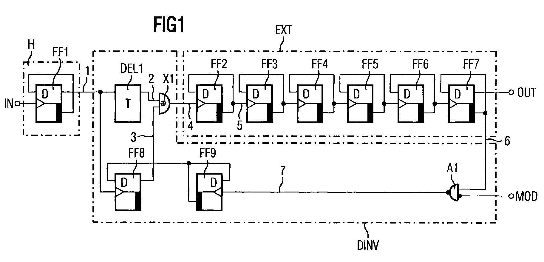
- FIG. 1 shows an example of a frequency divider for the division factors 1/128 and 1/129 indicated, this one input-side frequency bisector H, a device for synchronized inversion (DINV) and a divider extension EXT has.
- the frequency halving H on the input side generated from an input signal IN with the frequency f Intermediate signal 1, which only has the frequency f / 2.
- the frequency bisector H shown in FIG. 1 here consists of a D flip-flop FF1 which can be triggered by positive edges, the inverted output of which is fed back to the input D, the clock input of which is connected to the input signal IN of the frequency divider and the non-inverted output of which is the intermediate signal 1 of the frequency f / 2 delivers.
- the intermediate signal 1 is fed to an input of a delay element DIN1 and a trigger input of a first holding element FF8.
- the output signal 2 of the delay element which has the same throughput time as the first hold element FF8, is fed to a first input and a non-inverted output signal of the first hold element FF8 is fed to a second input of the EXOR gate X1, the output of which supplies the clock signal 4 for the divider extension.
- the divider extension EXT consists of flip-flops FF2 to FF7 and forms an asynchronous frequency divider with the division factor 1/2 6 .
- the EXOR gate serves as a controlled inverter, the intermediate signal 1 unchanged forming the clock signal 4 for the flip-flop FF2 when the second input is low. In contrast, when the level is high, the EXOR gate X1 inverts the clock signal 4 of the flip-flop F2.
- the state of the flip-flop FF8 decides whether the signal 2 is inverted or not. As long as the control signal MOD is high, the output of the NAND circuit A1 remains high and the flip-flops FF8 and FF9 also maintain their respective state.
- the flip-flops FF1 to FF7 therefore work as frequency dividers with the division factor 1/2 7 or 1/128. If the control signal MOD has a low level, the flip-flop FF9 and thus also the flip-flop FF8 change its state at each clock period of the output signal OUT.
- any change in the output of the flip-flop FF8 causes the clock signal 4 to be inverted with respect to the previous state, which corresponds to a phase shift of 180 °. Since the frequency at the input of the flip-flop FF2 is half as high as at the input of the frequency divider, this corresponds to a phase shift of 360 ° or a period based on the input frequency. This shift by one period causes the desired switching of the division factor from 1/128 to 1/129.
- Figure 2 shows a timing diagram of the signals 2 ... 5, wherein the signal 2 due to the high frequency is no longer rectangular, but approximately sinusoidal and has the period T.
- the signal 3 switches from a high level to a low level at a time t 1 .
- the signal 4 has a phase jump of 180 ° at the time t1.
- the signal 5 at the output of the flip-flop FF2 therefore changes from high to low only after a delay.
- the delay corresponds to exactly one period of the input frequency.
- the flip-flop FF8 ensures that the inversion takes place exactly at the zero crossing of signal 2. This is necessary to prevent the occurrence of short interference pulses in the output signal 4 of the EXOR gate at the time of the changeover.
- the flip-flop FF8 is therefore triggered by the intermediate signal 1.
- the delay element DEL1 simulates the throughput time of the flip-flop FF8, so that a level change of the flip-flop FF8 always coincides with a level change of the signal 2.
Landscapes
- Manipulation Of Pulses (AREA)
- Stabilization Of Oscillater, Synchronisation, Frequency Synthesizers (AREA)
- Mobile Radio Communication Systems (AREA)
Abstract
Der Anmeldungsgegenstand betrifft einen Frequenzteiler mit
einem zwischen 1/N und 1/(N+1) umschaltbaren Teilungsfaktor
und einer Eingangsfrequenz von ca. 1 Ghz, wie er beispielsweise
in mobilen Telekommunikationssystemen (GSM- oder DECT-Telefon)
vorkommt. Der hierdurch erzielte geringe Stromverbrauch
resultiert in erster Linie daraus, daß nur das Eingangs-Flipflop
(FF1) die relativ hohe Eingangsfrequenz verarbeiten
muß und ein Zwischensignal (1) mit der halben Frequenz
entweder direkt oder invertiert einer Teilererweiterung (EXT)
zugeführt wird.
Description
Unter dem Begriff Frequenzteiler sollen hier insbesondere sogenannte

Beispiele für die Verwendung und den Aufbau solcher Prescaler sind aus dem IEEE Journal of Solid-State Circuits, Vol. 29, No. 10, Oktober 1994, p. 1206 bis 1211 sowie Vol. 27, No. 12, Dezember 1992, p. 1794 bis 1798, bekannt, wobei jeweils einem synchronen 1:4/5-Teiler weitere asynchrone Teilererweiterungsstufen nachgeschaltet sind.Examples of the use and structure of such prescaler are from the IEEE Journal of Solid-State Circuits, Vol. 29, No. October 10, 1994, p. 1206 to 1211 and vol. 27, no. 12, December 1992, p. 1794 to 1798, known, one each synchronous 1: 4/5 divider further asynchronous divider expansion levels are connected downstream.
Die der Erfindung zugrundeliegende Aufgabe besteht nun darin,
einen Frequenzteiler der oben angegebenen Art anzugeben, der
einen besonders geringen Stromverbrauch aufweist. Diese Aufgabe
wird anhand der Merkmale des Patentanspruchs 1 gelöst.
Der Patentanspruch 2 betrifft eine vorteilhafte Ausgestaltung
der Erfindung, wobei ein Vorteil beispielsweise darin liegt,
daß nur das Ausgangssignal einer Stufe des Erweiterungsteilers
für das Umschalten zwischen dem Teilungsfaktor 1/N und
1/(N+1) verwendet wird und somit Strom und Chipfläche gespart
wird.The object on which the invention is based is now
specify a frequency divider of the type specified above, the
has a particularly low power consumption. This task
is solved based on the features of claim 1.
Im folgenden wird anhand der Zeichnung ein bevorzugtes Ausführungsbeispiel der Erfindung näher erläutert. Dabei zeigt
- Figur 1
- ein Schaltbild des bevorzugten Ausführungsbeispiels und
Figur 2- Zeitdiagramme zur Erläuterung der Funktionsweise der Schaltung nach Figur 1.
- Figure 1
- a circuit diagram of the preferred embodiment and
- Figure 2
- Time diagrams for explaining the mode of operation of the circuit according to FIG. 1.
Bei der Erfindung wird kein sonst üblicher synchroner 1:4/5-Teiler am Eingang verwendet, sondern zunächst aus dem Eingangssignal IN mit der Frequenz f ein Zwischensignal mit der Frequenz f/2 gebildet. Dies hat zur Folge, daß nicht drei Flipflops, sondern nur ein Flipflop mit der maximalen Frequenz f betrieben werden und somit bei den angegebenen Werten für N der Stromverbrauch wesentlich veringert werden kann.In the invention there is no otherwise common synchronous 1: 4/5 divider used at the input, but first from the input signal IN with the frequency f an intermediate signal with the Frequency f / 2 formed. As a result, not three Flip-flops, just a flip-flop with the maximum frequency f are operated and thus at the specified values for N the power consumption can be significantly reduced.
In Figur 1 ist beispielhaft ein Frequenzteiler für die Teilungsfaktoren 1/128 und 1/129 angegeben, wobei dieser einen eingangsseitigen Frequenzhalbierer H, eine Einrichtung zur synchronisierten Invertierung (DINV) und eine Teilererweiterung EXT aufweist. Der eingangsseitige Frequenzhalbierer H erzeugt aus einem Eingangssignal IN mit der Frequenz f ein Zwischensignal 1, das lediglich die Frequenz f/2 aufweist. In der Einrichtung DINV wird abhängig von einem Steuersignal MOD im Falle eines gewünschten Teilungsfaktors 1/N = 1/128 direkt auf einen Takteingang einer ersten Stufe der Teilererweiterung EXT durchgeschaltet, der ein Taktsignal 4 führt. Falls der Teilungsfaktor 1/(N + 1) = 1/129 gewünscht wird, wird durch das Steuersignal MOD das Zwischensignal 1 nach N Perioden invertiert und dadurch um die halbe Periodendauer des Zwischensignals 1 verzögert auf den Takteingang der Teilererweiterung durchgeschaltet. Das Ausgangssignal OUT wird in beiden Fällen vom Ausgang der letzten Stufe FF7 der Teilererweiterung EXT abgenommen.FIG. 1 shows an example of a frequency divider for the division factors 1/128 and 1/129 indicated, this one input-side frequency bisector H, a device for synchronized inversion (DINV) and a divider extension EXT has. The frequency halving H on the input side generated from an input signal IN with the frequency f Intermediate signal 1, which only has the frequency f / 2. In the DINV device is dependent on a control signal MOD in the case of a desired division factor 1 / N = 1/128 directly to a clock input of a first stage of the divider expansion EXT switched through, which carries a clock signal 4. If the division factor 1 / (N + 1) = 1/129 is desired by the control signal MOD the intermediate signal 1 after N periods inverted and thereby by half the period of the Intermediate signal 1 delays to the clock input of the divider extension switched through. The output signal OUT is in both cases from the output of the last stage FF7 of the divider extension EXT removed.
Der in Figur 1 dargestellte Frequenzhalbierer H besteht hier
aus einem durch positive Flanken triggerbaren D-Flipflop FF1,
dessen invertierter Ausgang auf den Eingang D rückgekoppelt
ist, dessen Takteingang mit dem Eingangssignal IN des Frequenzteilers
beschaltet ist und dessen nicht invertierter
Ausgang das Zwischensignal 1 der Frequenz f/2 liefert. Das
Zwischensignal 1 wird einem Eingang eines Verzögerungsglieds
DIN1 und einem Triggereingang eines ersten Halteglieds FF8
zugeführt. Das Ausgangssignal 2 des Verzögerungsglieds, das
dieselbe Durchlaufzeit wie das erste Halteglied FF8 aufweist,
ist einem ersten Eingang und ein nicht invertiertes Ausgangssignal
des ersten Haltegliedes FF8 einem zweiten Eingang des
EXOR-Gatters X1 zugeführt, dessen Ausgang das Taktsignal 4
für die Teilererweiterung liefert. Die Teilererweiterung EXT
besteht hierbei aus Flipflops FF2 bis FF7 und bildet einen
asynchronen Frequenzteiler mit dem Teilungsfaktor 1/26. Das
EXOR-Gatter dient hierbei als gesteuerter Inverter, wobei bei
Low-Pegel am zweiten Eingang das Zwischensignal 1 unverändert
das Taktsignal 4 für das Flipflop FF2 bildet. Bei High-Pegel
hingegen invertiert das EXOR-Gatter X1 das Taktsignal 4 des
Flipflops F2. Da der zweite Eingang des EXOR-Gatters mit dem
Ausgang des Flipflops FF8 verbunden ist, entscheidet der Zustand
des Flipflops FF8, ob das Signal 2 invertiert wird oder
nicht. Solange das Steuersignal MOD High-Pegel aufweist,
bleibt der Ausgang der NAND-Schaltung A1 auf High und damit
behalten auch die Flipflops FF8 und FF9 ihren jeweiligen Zustand
bei. Die Flipflops FF1 bis FF7 arbeiten daher als Frequenzteiler
mit dem Teilungsfaktor 1/27 bzw. 1/128. Weist das
Steuersignal MOD Low-Pegel auf, ändert bei jeder Taktperiode
des Ausgangssignals OUT das Flipflop FF9 und damit auch das
Flipflop FF8 seinen Zustand. Jede Änderung am Ausgang des
Flipflops FF8 bewirkt eine Invertierung des Taktsignals 4 bezogen
auf den vorhergehenden Zustand, was einer Phasenverschiebung
um 180° entspricht. Da die Frequenz am Eingang des
Flipflops FF2 halb so groß ist wie am Eingang des Frequenzteilers
entspricht das einer Phasenverschiebung um 360° oder
einer Periode bezogen auf die Eingangsfrequenz. Diese Verschiebung
um eine Periode bewirkt die gewünschte Umschaltung
des Teilungsfaktors von 1/128 auf 1/129.The frequency bisector H shown in FIG. 1 here consists of a D flip-flop FF1 which can be triggered by positive edges, the inverted output of which is fed back to the input D, the clock input of which is connected to the input signal IN of the frequency divider and the non-inverted output of which is the intermediate signal 1 of the frequency f / 2 delivers. The intermediate signal 1 is fed to an input of a delay element DIN1 and a trigger input of a first holding element FF8. The
Figur 2 zeigt ein Zeitdiagramm der Signale 2 ... 5, wobei das
Signal 2 wegen der hohen Frequenz nicht mehr rechteckförmig,
sondern annähernd sinusförmig ist und die Periodendauer T
aufweist. Das Signal 3 schaltet zu einem Zeitpunkt t1 von einem
Highpegel auf einen Lowpegel um. Das Signal 4 weist zum
Zeitpunkt t1 einen Phasensprung von 180° auf. Das Signal 5 am
Ausgang des Flipflops FF2 wechselt daher erst verzögert von
High auf Low. Die Verzögerung entspricht dabei genau einer
Periode der Eingangsfrequenz. Das Flipflop FF8 stellt sicher,
daß die Invertierung genau im Nulldurchgang des Signals 2
stattfindet. Dies ist erforderlich, um das Auftreten von kurzen
Störimpulsen im Ausgangssignal 4 des EXOR-Gatters im Umschaltzeitpunkt
zu verhindern. Das Flipflop FF8 wird deshalb
vom Zwischensignal 1 getriggert. Das Verzögerungselement DEL1
bildet die Durchlaufzeit des Flipflops FF8 nach, so daß ein
Pegelwechsel des Flipflops FF8 immer zeitlich mit einem Pegelwechsel
des Signals 2 zusammenfällt.Figure 2 shows a timing diagram of the
Claims (2)
Applications Claiming Priority (2)
| Application Number | Priority Date | Filing Date | Title |
|---|---|---|---|
| DE19741208 | 1997-09-18 | ||
| DE19741208 | 1997-09-18 |
Publications (3)
| Publication Number | Publication Date |
|---|---|
| EP0903858A2 true EP0903858A2 (en) | 1999-03-24 |
| EP0903858A3 EP0903858A3 (en) | 1999-12-22 |
| EP0903858B1 EP0903858B1 (en) | 2004-12-22 |
Family
ID=7842837
Family Applications (1)
| Application Number | Title | Priority Date | Filing Date |
|---|---|---|---|
| EP98116858A Expired - Lifetime EP0903858B1 (en) | 1997-09-18 | 1998-09-07 | Low-consumption frequency divider |
Country Status (3)
| Country | Link |
|---|---|
| US (1) | US5969548A (en) |
| EP (1) | EP0903858B1 (en) |
| DE (1) | DE59812404D1 (en) |
Cited By (2)
| Publication number | Priority date | Publication date | Assignee | Title |
|---|---|---|---|---|
| DE19930179A1 (en) * | 1999-06-30 | 2001-01-25 | Infineon Technologies Ag | High speed counter |
| CN104113325A (en) * | 2013-04-19 | 2014-10-22 | 中兴通讯股份有限公司 | Multi-mode programmable frequency divider |
Families Citing this family (6)
| Publication number | Priority date | Publication date | Assignee | Title |
|---|---|---|---|---|
| TW442951B (en) * | 1999-10-07 | 2001-06-23 | Nat Science Council | A low-voltage prescaler using dynamic back-gate forward bias method |
| JP2003152530A (en) * | 2001-11-13 | 2003-05-23 | Mitsubishi Electric Corp | Frequency divider |
| JP4077483B2 (en) * | 2003-05-20 | 2008-04-16 | 日本電信電話株式会社 | Variable frequency dividing method and variable frequency divider |
| US6822491B1 (en) * | 2003-06-27 | 2004-11-23 | Intel Corporation | Frequency prescaler apparatus, method, and system |
| US8471608B2 (en) * | 2011-02-02 | 2013-06-25 | Texas Instruments Incorporated | Clock divider circuit |
| US10407011B2 (en) | 2014-07-09 | 2019-09-10 | Magna International Inc. | Cast bumper system and method of manufacturing same |
Family Cites Families (6)
| Publication number | Priority date | Publication date | Assignee | Title |
|---|---|---|---|---|
| DE2935907B1 (en) * | 1979-09-05 | 1981-02-26 | Siemens Ag | Circuit arrangement for generating a symmetrical output signal |
| US4575867A (en) * | 1982-08-09 | 1986-03-11 | Rockwell International Corporation | High speed programmable prescaler |
| US4516251A (en) * | 1983-06-06 | 1985-05-07 | Motorola, Inc. | Programmable prescaler |
| DE3324506A1 (en) * | 1983-07-07 | 1985-01-17 | Telefunken Fernseh Und Rundfunk Gmbh, 3000 Hannover | Frequency divider with odd-numbered divider ratio |
| US4953187A (en) * | 1989-01-23 | 1990-08-28 | Motorola, Inc. | High speed prescaler |
| US4991187A (en) * | 1989-07-21 | 1991-02-05 | Motorola, Inc. | High speed prescaler |
-
1998
- 1998-09-07 EP EP98116858A patent/EP0903858B1/en not_active Expired - Lifetime
- 1998-09-07 DE DE59812404T patent/DE59812404D1/en not_active Expired - Fee Related
- 1998-09-18 US US09/157,037 patent/US5969548A/en not_active Expired - Fee Related
Cited By (4)
| Publication number | Priority date | Publication date | Assignee | Title |
|---|---|---|---|---|
| DE19930179A1 (en) * | 1999-06-30 | 2001-01-25 | Infineon Technologies Ag | High speed counter |
| DE19930179C2 (en) * | 1999-06-30 | 2001-07-05 | Infineon Technologies Ag | High speed counter |
| CN104113325A (en) * | 2013-04-19 | 2014-10-22 | 中兴通讯股份有限公司 | Multi-mode programmable frequency divider |
| CN104113325B (en) * | 2013-04-19 | 2018-09-28 | 南京中兴软件有限责任公司 | A kind of multi-mode programmable frequency divider |
Also Published As
| Publication number | Publication date |
|---|---|
| EP0903858B1 (en) | 2004-12-22 |
| EP0903858A3 (en) | 1999-12-22 |
| DE59812404D1 (en) | 2005-01-27 |
| US5969548A (en) | 1999-10-19 |
Similar Documents
| Publication | Publication Date | Title |
|---|---|---|
| DE60224478T2 (en) | Circuit for serializing synchronous data | |
| DE3411871C2 (en) | Variable frequency divider | |
| DE69414989T2 (en) | Digital phase-modulated clock generator enables reduced RF interference | |
| DE3307782A1 (en) | CIRCUIT ARRANGEMENT FOR GENERATING SYNCHRONOUS SIGNAL SIGNALS | |
| DE19625185C2 (en) | Precision clock | |
| DE10251703B4 (en) | Circuit arrangement for frequency division and phase locked loop with the circuit arrangement | |
| DE10064206B4 (en) | Delay lock loop for use with semiconductor memory devices | |
| EP0903859B1 (en) | Low-consumption frequency divider | |
| DE60217847T2 (en) | CIRCUIT FOR GENERATING A MULTI-PHASE CLOCK SIGNAL | |
| EP0903858B1 (en) | Low-consumption frequency divider | |
| DE3853980T2 (en) | Clock control for high speed digital integrated circuit. | |
| DE69803687T2 (en) | FREQUENCY DIVIDER WITH VARIABLE MODULUS | |
| DE102005051770A1 (en) | Method and apparatus for switching the frequency of a system clock | |
| DE19811591C2 (en) | Clock signal modeling circuit with negative delay | |
| DE10231186B4 (en) | frequency divider | |
| DE68925799T2 (en) | Toggle switch permitting a metastable state | |
| DE19819240C2 (en) | Semiconductor device | |
| DE10156817C1 (en) | Multi-phase comparator | |
| DE102005013497A1 (en) | Controllable frequency divider circuit for transceivers has signal input for supply of clock signal whereby first flip flop circuit is provided with clock input, which is coupled with signal input | |
| DE69827325T2 (en) | Method for frequency multiplication of a clock signal with duty cycle control and corresponding device | |
| DE102004001030A1 (en) | Nested high-resolution delay chain | |
| EP0448744A1 (en) | Clock synchronization circuit | |
| DE10013633A1 (en) | Static frequency divider with switchable division ratio prevents metastable states using two D=type flip-flops with alternately activatable inputs | |
| DE102004010405A1 (en) | Frequency divider circuit with controllable frequency divider ratio and method for frequency division in a frequency divider circuit | |
| EP0393341B1 (en) | Method and arrangement for converting an interrupted read-in clock into an uninterrupted read-out clock |
Legal Events
| Date | Code | Title | Description |
|---|---|---|---|
| PUAI | Public reference made under article 153(3) epc to a published international application that has entered the european phase |
Free format text: ORIGINAL CODE: 0009012 |
|
| AK | Designated contracting states |
Kind code of ref document: A2 Designated state(s): DE FR GB SE |
|
| AX | Request for extension of the european patent |
Free format text: AL;LT;LV;MK;RO;SI |
|
| PUAL | Search report despatched |
Free format text: ORIGINAL CODE: 0009013 |
|
| AK | Designated contracting states |
Kind code of ref document: A3 Designated state(s): AT BE CH CY DE DK ES FI FR GB GR IE IT LI LU MC NL PT SE |
|
| AX | Request for extension of the european patent |
Free format text: AL;LT;LV;MK;RO;SI |
|
| 17P | Request for examination filed |
Effective date: 20000121 |
|
| AKX | Designation fees paid |
Free format text: DE FR GB SE |
|
| RAP1 | Party data changed (applicant data changed or rights of an application transferred) |
Owner name: INFINEON TECHNOLOGIES AG |
|
| 17Q | First examination report despatched |
Effective date: 20040114 |
|
| GRAP | Despatch of communication of intention to grant a patent |
Free format text: ORIGINAL CODE: EPIDOSNIGR1 |
|
| GRAS | Grant fee paid |
Free format text: ORIGINAL CODE: EPIDOSNIGR3 |
|
| GRAA | (expected) grant |
Free format text: ORIGINAL CODE: 0009210 |
|
| AK | Designated contracting states |
Kind code of ref document: B1 Designated state(s): DE FR GB SE |
|
| PG25 | Lapsed in a contracting state [announced via postgrant information from national office to epo] |
Ref country code: GB Free format text: LAPSE BECAUSE OF FAILURE TO SUBMIT A TRANSLATION OF THE DESCRIPTION OR TO PAY THE FEE WITHIN THE PRESCRIBED TIME-LIMIT Effective date: 20041222 Ref country code: FR Free format text: LAPSE BECAUSE OF FAILURE TO SUBMIT A TRANSLATION OF THE DESCRIPTION OR TO PAY THE FEE WITHIN THE PRESCRIBED TIME-LIMIT Effective date: 20041222 |
|
| REG | Reference to a national code |
Ref country code: GB Ref legal event code: FG4D Free format text: NOT ENGLISH |
|
| REF | Corresponds to: |
Ref document number: 59812404 Country of ref document: DE Date of ref document: 20050127 Kind code of ref document: P |
|
| PG25 | Lapsed in a contracting state [announced via postgrant information from national office to epo] |
Ref country code: SE Free format text: LAPSE BECAUSE OF FAILURE TO SUBMIT A TRANSLATION OF THE DESCRIPTION OR TO PAY THE FEE WITHIN THE PRESCRIBED TIME-LIMIT Effective date: 20050322 |
|
| GBV | Gb: ep patent (uk) treated as always having been void in accordance with gb section 77(7)/1977 [no translation filed] |
Effective date: 20041222 |
|
| PLBE | No opposition filed within time limit |
Free format text: ORIGINAL CODE: 0009261 |
|
| STAA | Information on the status of an ep patent application or granted ep patent |
Free format text: STATUS: NO OPPOSITION FILED WITHIN TIME LIMIT |
|
| 26N | No opposition filed |
Effective date: 20050923 |
|
| EN | Fr: translation not filed | ||
| PGFP | Annual fee paid to national office [announced via postgrant information from national office to epo] |
Ref country code: DE Payment date: 20071113 Year of fee payment: 10 |
|
| PG25 | Lapsed in a contracting state [announced via postgrant information from national office to epo] |
Ref country code: DE Free format text: LAPSE BECAUSE OF NON-PAYMENT OF DUE FEES Effective date: 20090401 |