EP0904651B1 - Detection de fin de paquet pour la memorisation des paquets multiples dans une memoire ram statique - Google Patents
Detection de fin de paquet pour la memorisation des paquets multiples dans une memoire ram statique Download PDFInfo
- Publication number
- EP0904651B1 EP0904651B1 EP97906496A EP97906496A EP0904651B1 EP 0904651 B1 EP0904651 B1 EP 0904651B1 EP 97906496 A EP97906496 A EP 97906496A EP 97906496 A EP97906496 A EP 97906496A EP 0904651 B1 EP0904651 B1 EP 0904651B1
- Authority
- EP
- European Patent Office
- Prior art keywords
- data
- memory
- memory location
- value
- written
- Prior art date
- Legal status (The legal status is an assumption and is not a legal conclusion. Google has not performed a legal analysis and makes no representation as to the accuracy of the status listed.)
- Expired - Lifetime
Links
- 238000001514 detection method Methods 0.000 title description 2
- 230000005540 biological transmission Effects 0.000 claims description 24
- 238000000034 method Methods 0.000 claims description 22
- 230000006870 function Effects 0.000 description 6
- 230000010365 information processing Effects 0.000 description 5
- 238000012986 modification Methods 0.000 description 4
- 230000004048 modification Effects 0.000 description 4
- 238000012546 transfer Methods 0.000 description 4
- 238000004891 communication Methods 0.000 description 3
- 239000004065 semiconductor Substances 0.000 description 2
- RYGMFSIKBFXOCR-UHFFFAOYSA-N Copper Chemical compound [Cu] RYGMFSIKBFXOCR-UHFFFAOYSA-N 0.000 description 1
- 101100172132 Mus musculus Eif3a gene Proteins 0.000 description 1
- 238000010276 construction Methods 0.000 description 1
- 229910052802 copper Inorganic materials 0.000 description 1
- 239000010949 copper Substances 0.000 description 1
- 230000001419 dependent effect Effects 0.000 description 1
- 238000013461 design Methods 0.000 description 1
- 238000012545 processing Methods 0.000 description 1
- 238000004088 simulation Methods 0.000 description 1
Images



Classifications
-
- H—ELECTRICITY
- H04—ELECTRIC COMMUNICATION TECHNIQUE
- H04L—TRANSMISSION OF DIGITAL INFORMATION, e.g. TELEGRAPHIC COMMUNICATION
- H04L49/00—Packet switching elements
- H04L49/90—Buffering arrangements
-
- H—ELECTRICITY
- H04—ELECTRIC COMMUNICATION TECHNIQUE
- H04L—TRANSMISSION OF DIGITAL INFORMATION, e.g. TELEGRAPHIC COMMUNICATION
- H04L9/00—Cryptographic mechanisms or cryptographic arrangements for secret or secure communications; Network security protocols
- H04L9/40—Network security protocols
Definitions
- This invention relates generally to a method and device for controlling the transmission of information by a station to and from an ethernet and, more particularly, to a method and device for increasing the performance ofthe transmission of information, and even more particularly, to a method and device for efficiently storing multiple packets of information in a memory device by identifying precisely the location of the end-of-packet in the memory device.
- EP-A-0 429 054 discloses a known data representation and protocol to interface to network.
- JP-A-62 216046 discloses a record control system for a logical simulation device.
- a local-area network is a communication system that enables personal computers, work stations, file servers, repeaters, data terminal equipment ("DTE”), and other such information processing equipment located within a limited geographical area such as an office, a building, or a cluster of buildings to electronically transfer information among one another.
- DTE data terminal equipment
- Each piece of information processing equipment in the LAN communicates with other information processing equipment in the LAN by following a fixed protocol (or standard) which defines the network operation.
- the ISO Open Systems Interconnection Basic Reference Model defines a seven-layer model for data communications in a LAN.
- the lowest layer in the model is the physical layer which consists of modules that specify (a) the physical media which interconnects the network nodes and over which data is to be electronically transmitted, (b) the manner in which the network nodes interface to the physical transmission media, (c) the process for transferring data over the physical media, and (d) the protocol of the data stream.
- IEEE Standard 802.3 Carrier Sense Multiple Access with Collision Detection (CSMA/CD) Access Method and Physical Layer Specifications, is one of the most widely used standards for the physical layer. Commonly referred to as Ethernet, IEEE Standard 802.3 deals with transferring data over twisted-pair cables or co-axial cables which are typically more expensive than twisted-pair cables. The 10Base-T protocol of IEEE Standard 802.3 prescribes a rate of 10 megabits/second ("Mbps") for transferring data over twisted-pair cables.
- Mbps megabits/second
- Figure 1 illustrates how a workstation, personal computer, file server, data terminal equipment, or other such information processing equipment, represented by CPU 12 , is connected to ethernet 22 or other types of data communications equipment represented by the media independent interface 24 .
- ethernet controller 14 also commonly known as a Network Interface Controller is situated between the CPU 12 and the incoming (and outgoing) ethernet 22 lines.
- the ethernet 22 consists of two pairs of twisted-pair copper cables, an incoming pair referred to as 10R and an outgoing pair referred to as 10T.
- the ethernet controller 14 is responsible for controlling the transmission of outgoing data to the outgoing pair or cable and the reception of incoming data from the incoming pair or cable.
- the outgoing data is Manchester encoded to reduce electromagnetic interference.
- the Manchester encoding causes some portions of the data stream to be pulses at 10 MHz while other portions of the data stream are pulses at 5 MHz.
- the ethernet controller 14 ( Figure 1) is responsible for controlling the transmission of data from the CPU 12 to the ethernet 22.
- One of the major problems confronted by the ethernet controller 14 is to control the transmission of data so there are minimal interruptions in transmission. For example, if there is an interruption in the transmission of data, the ethernet system then must stop and retransmit all of the data. This means that the transmitting station must retransmit the data if the receiving station is interrupted and cannot continue to receive data.
- the present invention teaches a method of providing a buffer for the temporary storage of incoming or outgoing data which are formatted into packets. For the most efficient storage of information in the form of packets into a buffer, which by necessity is as small as possible for both space reasons and cost reasons, it is desirable to store the packets contiguously, that is, without any unfilled memory locations between packets.
- What is needed is a method of detecting the end-of-packet of a sequence of bytes, or other units of data in a packet, and to identify the last memory location into which the sequence was written to allow sequential storage of the next packet so that multiple packets of information can be efficiently stored in a memory device.
- a method of precisely identifying the end-of-packet location in a memory device used as a buffer during the transmission of packets of data from one location to another is utilized as a buffer.
- a first location in the memory device is reserved and a sequence of data is written sequentially into the memory device.
- the address of the memory location in which the last byte is written is written to the first reserved location.
- the last byte of data in the packet is identified by inputting into a counter the number of bytes that is contained in the packet.
- the counter is incremented as each byte is written into a memory location.
- a write pointer is updated with the memory location into which data is being written. The contents of the write pointer is written to the reserved first memory when the counter reaches the inputted number of bytes.
- a second memory location in the memory device is reserved immediately following the first reserved memory location and the value HEX0000 is written into the second reserved location.
- the data is then written into the memory device starting with the first memory location following the second reserved location.
- the write counter When the write counter reaches the inputted number of bytes the value in the second reserved location is changed from the value HEX0000 to the value HEX1000.
- the data is read from the memory device.
- the value contained in the first reserved memory device is written to a first register and the most significant bit in the second reserved register is written to a second register.
- the value in the first register is compared to a value in a read pointer and a logic TRUE or a logic FALSE obtained. If the value in the second register is TRUE and the value in the first register is TRUE the end of packet has been detected.
- the read pointer In the event the end of packet has not been written the read pointer is prevented from going past the write pointer by incrementing a value in a third register when a memory location has been written and decrementing the value in the third register when a memory location has been read.
- the value in the third register is zero, an EMPTY flag is set and read is inhibited.
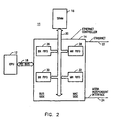
- FIG. 1 there is shown a prior art system 10 with a CPU 12 , and an ethernet controller 14 with connections to an ethernet 22 and a media independent interface 24 .
- the CPU 12 is connected to the ethernet controller by BUS 17 .
- System 11 includes an SRAM 16 connected externally to the ethernet controller 14 and the CPU 12 .
- SRAM 16 connected externally to the ethernet controller 14 and the CPU 12 .
- This construction is to allow the ethernet controller 14 semiconductor device to be as small as possible and to allow the flexibility for the design engineer to provide a larger buffer if necessary.
- the SRAM 16 could be designed as part of the ethernet controller 14 device.
- the CPU 12, the ethernet controller 14, and the SRAM 16 could all be designed as a single semiconductor device.
- the function of the illustrated portion of the ethernet controller 14 is to manage the transmission of data to and from the ethernet 22 and the media independent interface 24.
- the ethernet controller 14 manages the transmission of data by utilizing SRAM 16 as a buffer to prevent the slowing down of the transmission of data to and from either the CPU 12 or the ethernet 22 or the media independent interface 24 .
- SRAM 16 as a buffer to prevent the slowing down of the transmission of data to and from either the CPU 12 or the ethernet 22 or the media independent interface 24 .
- the transmission of data can be slowed down, for example, the latency of CPU 12 can be high and the transmission of data from the ethernet 22 could be stopped until CPU 12 is freed from other interrupts.
- the CPU 12 could be attempting to send data via the ethernet 22 and the ethernet 22 could be busy which would cause the data from the CPU 22 to be stopped or held until the ethernet 22 is free.
- the ethernet controller 14 has four FIFOs, a BX FIFO 26, an MX FIFO 28, a BR FIFO 30, and an MR FIFO 32.
- the BX FIFO 26 and BR FIFO 30 are on the bus side of ethernet controller 14 and MX FIFO 28 and MR FIFO 32 are on the Media Access Control (MAC) side of the ethernet controller 14.
- Each of the FIFOs controls either an input or output function.
- the BX FIFO 26 controls the transmission of data from CPU 12 to SRAM 16.
- MX FIFO 28 controls the transmission of data from SRAM 16 to the ethernet 22 or the media independent interface 24.
- MR FIFO 32 controls the transmission of data from either the ethernet 22 or the media independent interface 24.
- ethernet 22 controls the transmission of data from either the ethernet 22 or the media independent interface 24.
- SRAM 16 controls the transmission of data from either the ethernet 22 or the media independent interface 24.
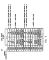
- FIG. 3 there is shown a memory portion 34 of a memory device such as SRAM 16. It is to be understood that other memory devices can be used without departing from the intended scope of this invention. Shown are 18 memory locations 36 with memory addresses 38 from HEX0000 to HEX0011. In this discussion, the convention is followed that memory locations are addressed by words, that is, each memory location has two 8 bit bytes, an upper byte location and a lower byte location. It should be understood that the portion 34 could be anywhere in SRAM 16 and that the addresses 38 could be any sequence of values within the maximum size of the memory. Shown in Figure 3 are two packets of data written into memory portion 34.
- the first packet is made up of 5 bytes, DATA 0 through DATA 4, and are shown in memory locations with addresses of HEX0002 through HEX0004. Because DATA 4 is the last byte of the first packet, that is, the end-of-packet, the address (HEX0004) of the memory location in which DATA 4 is written is written into a first reserved memory location, in this case, the memory location with an address of HEX0000. Because the last byte in the first packet has been written, the contents of a second reserved memory location, in this case, the memory location with an address of HEX0001 is changed to HEX1000. The value HEX1000 indicates that the packet is valid and will be discussed in more detail below.
- the first two reserved locations in the portion of the memory in which memory is to be written are memory locations HEX0000 and HEX0001.
- the location of each pair of reserved locations is dependent upon the sizes of the preceding packets stored in the memory.
- the first reserved location is memory location HEX0009 and the second reserved location is memory location HEX000A.
- the 32 bit STATUS for the second packet is written into memory locations HEX000F and HEX0010 and the 32 bit DESCRIPTOR for the second packet is written into memory locations HEX0011 and HEX0012.
- the 32 bit STATUS and DESCRIPTOR for each packet contain information concerning the packet and are not described in detail.
- the CPU 12 When the CPU 12 wishes to transmit data it will request the applicable bus, in this case the PCI BUS 18, and inform BX FIFO 26 that it has a certain number of bytes of data to transmit. This number is communicated to a counter 42 . There is shown the value of 5 written into the counter 42 . A five byte packet is being used as an example and will be explained below in conjunction with Figure 5. The counter 42 is incremented when a memory location is written and when the incremented value is equal to the value input from BX FIFO 26 it indicates that the value just written into memory is the last byte of data in the packet.
- the value representing the number of bytes contained in a packet could be input to counter 42 and counter 42 could be decremented as each byte of data is written and when the value zero is reached it would be indicated that the last byte of data has been written into memory, that is, the end-of-packet has been written.
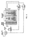
- Figure 4 illustrates a situation in which the end-of-packet has not been reached.
- the initial step is to reserve the first two available locations in memory, and for explanation purposes they are shown as memory locations HEX0000 at 43 and HEX0001 at 45.
- the write pointer WR PTR 44 will initially be pointing to memory location HEX0000 at 43.
- the contents of memory location HEX0000 43 will be written to a register MX EOP 46 if the value in TX OWN 48 is a zero.
- the contents of HEX0000 are shown as XXXX which indicates "don't cares" since it doesn't make any difference what value is in HEX0000 until a valid end-of-packet location is written into it.
- the write pointer WR PTR 44 will be incremented and will point to memory location HEX0001 at 45.
- the value HEX0000 will be written into the second reserved memory location HEX0001 at 45.
- the WR PTR 44 would read HEX0001, and counter 42 would not have been incremented or decremented because no data has been written.
- the WR PTR 44 would increment and the first and second bytes of data, DATA 0 and DATA 1, at 50, will be written into memory location HEX0002 and the counter 42 would be incremented to 2. This will repeat until the situation shown in Figure 4 is reached.
- the WR PTR 44 is pointing to memory location HEX0003 and DATA 2 at 52 has been written into the lower byte memory location HEX0003 and counter 42 has been incremented to the value 4 indicating that either 3 or 4 bytes of data have been written into memory.
- the value HEX1000 in the second reserved memory location indicates that the packet is valid, that is, the end-of-packet has been written and the value in the first reserved memory location (HEX0000 in this case) is the memory location in which the end-packet-is written.
- FIG. 6 there is illustrated the method of reading the data in a packet when the end-of-packet has been written into memory.
- Figure 6 shows the packet that was written into memory as shown in Figure 5 .
- the packet contains 5 bytes of data that have been written into memory location HEX0002 through the lower byte location of memory location HEX0004. Because the end-of-packet has been written into memory, the first reserved memory location (HEX0000) has been written with the memory location of the last byte in the packet, that is, the location of the end-of-packet. In this case, the memory location of the last byte is memory location HEX0004.
- This value, HEX0004, is also written into register MX EOP 46 when the read pointer RE PTR 54 points to the first reserved memory location, in this case, memory location HEX0000.
- the next step is when RD PTR 54 is pointing at the second reserved memory location, in this case, memory location HEX0001.
- the contents of the second reserved memory location will contain the value HEX1000 because the end-of-packet has been written into memory.
- the value contained in register MX EOP 46 is input to a comparator circuit at 56.
- the contents of RE PTR 54 is also input to comparator circuit 56 where it is compared to the contents of register MX EOP 46.
- TX OWN 48 is TRUE (that is, a 1) and the output of the comparator circuit 56 is TRUE the end-of-packet has been reached as indicated at 58 .
- TX OWN 48 is TRUE (that is, a 1) and the output of the comparator circuit 56 is TRUE the end-of-packet has been reached as indicated at 58 .
- TX OWN 48 is TRUE (that is, a 1) and the output of the comparator circuit 56 is TRUE the end-of-packet has been reached as indicated at 58 .
- TX OWN 48 is TRUE (that is, a 1) and the output of the comparator circuit 56 is TRUE the end-of-packet has been reached as indicated at 58 .
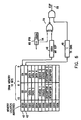
- FIG. 7 there is illustrated the situation in which the end-of-packet has not been written into memory and to save time the system allows the reading of the data that has been written into memory.
- the read pointer does not pass the write pointer and begin reading garbage.
- the situation as illustrated in Figure 7 is that the end-of-packet for the packet being written into memory has not been reached, however, reading the data has begun and is allowed to begin for the sake of efficiency. For example, there are situations where the packets are much longer than the examples discussed in which case it would not be efficient for the read function to wait until a long packet is completely written before reading is begun.
- the read pointer points to the first reserved memory location at 43
- the contents of the first reserved memory location will be written into register MX EOP 46 .
- the RE PTR 54 then points to the second reserved memory location at 45 and the most significant bit of the value contained in the second reserved memory location will be written to the register TX OWN 48. Because the most significant bit is a zero the comparator circuit at 56 will indicate a FALSE at 58 which indicates a NOT EOP.
- a register 60 that is incremented each time a data value is written into memory as indicated by WR PTR 44 and is decremented each time a data value is read from memory as indicated by RD PTR 54.
- the WR PTR 44 is pointing to memory location HEX0004 which indicates that a data value has just been written to memory location HEX0004 and the RD PTR 54 is also pointing to memory location HEX0004 which indicates that the data value in memory location HEX0004 has just been read.
- the value in register 60 will be zero and an EMPTY flag in register 62 will be set which will prevent any further reading of data from memory.
- the value in register 60 will be incremented, at this point the value in register 60 will be 1, the flag in register 62 will be reset and the RD PTR 54 will be allowed to increment and the data in the next memory location will be allowed to be read. If there has not been any further data written into memory, the register 60 will again contain the value zero and read will again be inhibited. As the WR PTR 44 is incremented and as data is written into memory the last byte will eventually be reached at which time the counter 42 ( Figures 4 and 5) will indicate this to WR PTR 44 and the value in the WR PTR 44 will be immediately written into MX EOP 46 and into the first reserved memory location 43.
Landscapes
- Engineering & Computer Science (AREA)
- Computer Networks & Wireless Communication (AREA)
- Signal Processing (AREA)
- Computer Security & Cryptography (AREA)
- Data Exchanges In Wide-Area Networks (AREA)
- Communication Control (AREA)
Claims (12)
- Procédé d'identification de la position de fin de paquet dans un dispositif de mémoire (16) utilisé comme tampon pendant la transmission d'au moins un paquet, comportant les étapes consistant à :réserver une première position de mémoire (43) dans le dispositif de mémoire (16) ;réserver une seconde position de mémoire (45) dans le dispositif de mémoire (16) suivant immédiatement la première position de mémoire réservée (43) et écrire la valeur HEX0000 dans la seconde position de mémoire ;écrire une séquence de données à partir d'au moins un paquet dans un nombre séquentiel de positions de mémoire (36) suivant la première position de mémoire réservée ;écrire dans la première position de mémoire réservée (43) l'adresse de la dernière position de mémoire dans laquelle la séquence de données a été écrite en incluant les étapes consistant à :introduire dans un compteur (42) un nombre de positions de mémoire séquentielles requis pour la séquence de données ;incrémenter le compteur (42) lorsque chaque position de mémoire est écrite ;actualiser un pointeur d'écriture (44) avec l'adresse de mémoire de la position de mémoire dans laquelle les données sont en cours d'écriture ; etécrire les contenus du pointeur d'écriture (44) dans la première position de mémoire réservée lorsque le compteur (42) atteint le nombre introduit de positions de mémoire séquentielles (36) requis.
- Procédé selon la revendication 1, dans lequel l'étape consistant à écrire une séquence de données à partir d'au moins un paquet dans un nombre séquentiel de positions de mémoire (36) est réalisée en écrivant la première séquence de données dans une position de mémoire suivant immédiatement la seconde position de mémoire réservée (45).
- Procédé selon la revendication 1 ou la revendication 2, comprenant, de plus, l'étape consistant à écrire HEX1000 dans la seconde position de mémoire réservée (45) lorsque le compteur (42) atteint le nombre introduit de positions séquentielles de mémoire requis.
- Procédé selon la revendication 3, comprenant, de plus, l'étape consistant à lire la séquence de données.
- Procédé selon la revendication 4 comprenant, de plus, l'étape consistant à écrire la valeur de la première position de mémoire réservée (43) dans un premier registre (46).
- Procédé selon la revendication 5, comprenant, de plus, l'étape consistant à écrire le binaire le plus significatif de la valeur de la seconde position de mémoire réservée (45) dans un second registre (48).
- Procédé selon la revendication 6, dans lequel l'étape consistant à lire la séquence de données, comprend les étapes consistant à :actualiser un pointeur de lecture (54) avec une adresse de mémoire de la position de mémoire à partir de laquelle les données doivent être lues ; etobtenir une première valeur logique en comparant l'adresse de mémoire du pointeur de lecture (54) avec la valeur contenue de la première position de mémoire réservée (43).
- Procédé selon la revendication 7, comprenant, de plus, l'étape consistant à indiquer un paquet de fin lorsque la première valeur logique est VRAIE et que la valeur contenue dans le second registre (48) est VRAIE.
- Procédé selon la revendication 8 comprenant, de plus, les étapes consistant à :incrémenter une valeur dans un troisième registre (60) lorsque des données sont écrites dans une position de mémoire ; etdécrémenter le troisième registre (60) lorsque des données sont lues à partir d'une position de mémoire.
- , Procédé selon la revendication 9, comprenant, de plus, l'étape consistant à établir un drapeau de vide si la valeur du troisième registre (60) présente une valeur nulle.
- Procédé selon la revendication 10, comprenant, de plus, l'étape consistant à établir un drapeau complet si la valeur du troisième registre (60) présente une valeur de HEXFFFF.
- Procédé selon la revendication 11 comprenant, de plus, l'étape consistant à empêcher l'étape de lecture d'une position de mémoire si le drapeau vide est établi.
Applications Claiming Priority (3)
| Application Number | Priority Date | Filing Date | Title |
|---|---|---|---|
| US08/659,795 US5819113A (en) | 1996-06-06 | 1996-06-06 | Method of identifying end of pocket by writing the address of last data into the first location of the memory |
| PCT/US1997/001857 WO1997047115A1 (fr) | 1996-06-06 | 1997-02-04 | Detection de fin de paquet pour la memorisation des paquets multiples dans une memoire ram statique |
| US659795 | 2000-09-12 |
Publications (2)
| Publication Number | Publication Date |
|---|---|
| EP0904651A1 EP0904651A1 (fr) | 1999-03-31 |
| EP0904651B1 true EP0904651B1 (fr) | 2003-10-15 |
Family
ID=24646877
Family Applications (1)
| Application Number | Title | Priority Date | Filing Date |
|---|---|---|---|
| EP97906496A Expired - Lifetime EP0904651B1 (fr) | 1996-06-06 | 1997-02-04 | Detection de fin de paquet pour la memorisation des paquets multiples dans une memoire ram statique |
Country Status (6)
| Country | Link |
|---|---|
| US (1) | US5819113A (fr) |
| EP (1) | EP0904651B1 (fr) |
| JP (1) | JP3811759B2 (fr) |
| DE (1) | DE69725570T2 (fr) |
| TW (1) | TW312768B (fr) |
| WO (1) | WO1997047115A1 (fr) |
Families Citing this family (2)
| Publication number | Priority date | Publication date | Assignee | Title |
|---|---|---|---|---|
| JPH1188441A (ja) * | 1997-09-12 | 1999-03-30 | Canon Inc | メモリ制御装置及び方法、送信装置、受信装置 |
| WO2002005554A1 (fr) * | 2000-07-12 | 2002-01-17 | Matsushita Electric Industrial Co., Ltd. | Dispositifs d'enregistrement et de lecture de donnees, procedes d'enregistrement et de lecture de donnees |
Family Cites Families (12)
| Publication number | Priority date | Publication date | Assignee | Title |
|---|---|---|---|---|
| JPS57210498A (en) * | 1981-06-19 | 1982-12-24 | Fujitsu Ltd | Data storage controller |
| JPS59160231A (ja) * | 1983-03-02 | 1984-09-10 | Canon Inc | オフライン記録装置 |
| US5133062A (en) * | 1986-03-06 | 1992-07-21 | Advanced Micro Devices, Inc. | RAM buffer controller for providing simulated first-in-first-out (FIFO) buffers in a random access memory |
| US4949301A (en) * | 1986-03-06 | 1990-08-14 | Advanced Micro Devices, Inc. | Improved pointer FIFO controller for converting a standard RAM into a simulated dual FIFO by controlling the RAM's address inputs |
| JPS62216046A (ja) * | 1986-03-17 | 1987-09-22 | Fujitsu Ltd | 論理シミユレ−シヨン装置の記録制御方式 |
| US4922438A (en) * | 1986-12-11 | 1990-05-01 | Siemens Aktiengesellschaft | Method and apparatus for reading packet-oriented data signals into and out of a buffer |
| FR2616604B1 (fr) * | 1987-06-15 | 1989-09-22 | Lespagnol Albert | Equipement de reconstitution et multiplexage de trames d'origines diverses constituees de paquets de longueur fixe en nombre variable |
| US4914652A (en) * | 1988-08-01 | 1990-04-03 | Advanced Micro Devices, Inc. | Method for transfer of data between a media access controller and buffer memory in a token ring network |
| US5495482A (en) * | 1989-09-29 | 1996-02-27 | Motorola Inc. | Packet transmission system and method utilizing both a data bus and dedicated control lines |
| US5175817A (en) * | 1989-11-20 | 1992-12-29 | Digital Equipment Corporation | Data representation protocol for communications between different networks |
| US5097261A (en) * | 1989-11-22 | 1992-03-17 | International Business Machines Corporation | Data compression for recording on a record medium |
| EP0632625B1 (fr) * | 1993-06-30 | 1996-10-30 | International Business Machines Corporation | Adapteur de communications programmable à haute performance pour réseaux de paquets à haut débit |
-
1996
- 1996-06-06 US US08/659,795 patent/US5819113A/en not_active Expired - Lifetime
- 1996-10-15 TW TW085112542A patent/TW312768B/zh active
-
1997
- 1997-02-04 JP JP50054298A patent/JP3811759B2/ja not_active Expired - Fee Related
- 1997-02-04 DE DE69725570T patent/DE69725570T2/de not_active Expired - Lifetime
- 1997-02-04 EP EP97906496A patent/EP0904651B1/fr not_active Expired - Lifetime
- 1997-02-04 WO PCT/US1997/001857 patent/WO1997047115A1/fr not_active Ceased
Also Published As
| Publication number | Publication date |
|---|---|
| JP3811759B2 (ja) | 2006-08-23 |
| DE69725570T2 (de) | 2004-07-29 |
| TW312768B (en) | 1997-08-11 |
| US5819113A (en) | 1998-10-06 |
| EP0904651A1 (fr) | 1999-03-31 |
| WO1997047115A1 (fr) | 1997-12-11 |
| JP2001502855A (ja) | 2001-02-27 |
| DE69725570D1 (de) | 2003-11-20 |
Similar Documents
| Publication | Publication Date | Title |
|---|---|---|
| EP0976054B1 (fr) | Generation d'adresse et arbitrage de trajet de donnees vers et depuis une memoire ram statique afin d'absorber des paquets multiples transmis | |
| US5247626A (en) | Fddi controller having flexible buffer management | |
| EP0459757B1 (fr) | Adaptateur de réseau | |
| US5878028A (en) | Data structure to support multiple transmit packets for high performance | |
| US4858112A (en) | Interface comprising message and protocol processors for interfacing digital data with a bus network | |
| EP0797335B1 (fr) | Interface de réseau | |
| US5764895A (en) | Method and apparatus for directing data packets in a local area network device having a plurality of ports interconnected by a high-speed communication bus | |
| EP0617368B1 (fr) | Processus d'arbitrage pour la commande du flux de données à travers d'un contrÔleur E/S | |
| US5210749A (en) | Configuration of srams as logical fifos for transmit and receive of packet data | |
| US6925512B2 (en) | Communication between two embedded processors | |
| US7149833B2 (en) | Method and apparatus for extending the range of the universal serial bus protocol | |
| US6980520B1 (en) | Method and apparatus for performing source-based flow control across multiple network devices | |
| US5933413A (en) | Adaptive priority determination for servicing transmit and receive in network controllers | |
| US6442168B1 (en) | High speed bus structure in a multi-port bridge for a local area network | |
| CN1095134C (zh) | 使用系统总线控制器的模块间通信的设备和方法 | |
| EP0904651B1 (fr) | Detection de fin de paquet pour la memorisation des paquets multiples dans une memoire ram statique | |
| US4612541A (en) | Data transmission system having high-speed transmission procedures | |
| US6396806B1 (en) | Transmission line duplexing processing method and apparatus thereof, and recording medium for recording its processing procedure | |
| US6954427B1 (en) | Method and apparatus for performing priority-based admission control | |
| KR100474658B1 (ko) | 다수의전송패킷들에대처하기위한어드레스생성및sram으로/으로부터의데이터경로조정 | |
| JP2001257686A (ja) | 計算機システム及び計算機システムのデータ通信方法 | |
| US20030172176A1 (en) | Embedded system having multiple data receiving channels | |
| CA2269961C (fr) | Procede et appareil pour augmenter l'etendue du protocole de bus serie universel lors de transferts asynchrones | |
| Protogeros et al. | Traffic analyser and generator Part 1: High-speed traffic capture for IEEE 802.3/Ethernet networks |
Legal Events
| Date | Code | Title | Description |
|---|---|---|---|
| PUAI | Public reference made under article 153(3) epc to a published international application that has entered the european phase |
Free format text: ORIGINAL CODE: 0009012 |
|
| 17P | Request for examination filed |
Effective date: 19981015 |
|
| AK | Designated contracting states |
Kind code of ref document: A1 Designated state(s): DE GB |
|
| GRAH | Despatch of communication of intention to grant a patent |
Free format text: ORIGINAL CODE: EPIDOS IGRA |
|
| GRAS | Grant fee paid |
Free format text: ORIGINAL CODE: EPIDOSNIGR3 |
|
| GRAA | (expected) grant |
Free format text: ORIGINAL CODE: 0009210 |
|
| AK | Designated contracting states |
Kind code of ref document: B1 Designated state(s): DE GB |
|
| REG | Reference to a national code |
Ref country code: GB Ref legal event code: FG4D |
|
| REF | Corresponds to: |
Ref document number: 69725570 Country of ref document: DE Date of ref document: 20031120 Kind code of ref document: P |
|
| PLBE | No opposition filed within time limit |
Free format text: ORIGINAL CODE: 0009261 |
|
| STAA | Information on the status of an ep patent application or granted ep patent |
Free format text: STATUS: NO OPPOSITION FILED WITHIN TIME LIMIT |
|
| 26N | No opposition filed |
Effective date: 20040716 |
|
| REG | Reference to a national code |
Ref country code: GB Ref legal event code: 732E Free format text: REGISTERED BETWEEN 20091210 AND 20091216 |
|
| PGFP | Annual fee paid to national office [announced via postgrant information from national office to epo] |
Ref country code: DE Payment date: 20110228 Year of fee payment: 15 |
|
| PGFP | Annual fee paid to national office [announced via postgrant information from national office to epo] |
Ref country code: GB Payment date: 20110124 Year of fee payment: 15 |
|
| GBPC | Gb: european patent ceased through non-payment of renewal fee |
Effective date: 20120204 |
|
| REG | Reference to a national code |
Ref country code: DE Ref legal event code: R119 Ref document number: 69725570 Country of ref document: DE Effective date: 20120901 |
|
| PG25 | Lapsed in a contracting state [announced via postgrant information from national office to epo] |
Ref country code: GB Free format text: LAPSE BECAUSE OF NON-PAYMENT OF DUE FEES Effective date: 20120204 |
|
| PG25 | Lapsed in a contracting state [announced via postgrant information from national office to epo] |
Ref country code: DE Free format text: LAPSE BECAUSE OF NON-PAYMENT OF DUE FEES Effective date: 20120901 |