EP0904938A1 - Technique d'impression et appareil d'impression - Google Patents
Technique d'impression et appareil d'impression Download PDFInfo
- Publication number
- EP0904938A1 EP0904938A1 EP97922072A EP97922072A EP0904938A1 EP 0904938 A1 EP0904938 A1 EP 0904938A1 EP 97922072 A EP97922072 A EP 97922072A EP 97922072 A EP97922072 A EP 97922072A EP 0904938 A1 EP0904938 A1 EP 0904938A1
- Authority
- EP
- European Patent Office
- Prior art keywords
- stencil
- printing
- induction heating
- electromagnetic induction
- paste
- Prior art date
- Legal status (The legal status is an assumption and is not a legal conclusion. Google has not performed a legal analysis and makes no representation as to the accuracy of the status listed.)
- Withdrawn
Links
Images








Classifications
-
- B—PERFORMING OPERATIONS; TRANSPORTING
- B41—PRINTING; LINING MACHINES; TYPEWRITERS; STAMPS
- B41F—PRINTING MACHINES OR PRESSES
- B41F15/00—Screen printers
- B41F15/08—Machines
- B41F15/0804—Machines for printing sheets
- B41F15/0813—Machines for printing sheets with flat screens
-
- B—PERFORMING OPERATIONS; TRANSPORTING
- B41—PRINTING; LINING MACHINES; TYPEWRITERS; STAMPS
- B41F—PRINTING MACHINES OR PRESSES
- B41F15/00—Screen printers
- B41F15/08—Machines
-
- B—PERFORMING OPERATIONS; TRANSPORTING
- B41—PRINTING; LINING MACHINES; TYPEWRITERS; STAMPS
- B41M—PRINTING, DUPLICATING, MARKING, OR COPYING PROCESSES; COLOUR PRINTING
- B41M1/00—Inking and printing with a printer's forme
- B41M1/12—Stencil printing; Silk-screen printing
-
- H—ELECTRICITY
- H05—ELECTRIC TECHNIQUES NOT OTHERWISE PROVIDED FOR
- H05K—PRINTED CIRCUITS; CASINGS OR CONSTRUCTIONAL DETAILS OF ELECTRIC APPARATUS; MANUFACTURE OF ASSEMBLAGES OF ELECTRICAL COMPONENTS
- H05K3/00—Apparatus or processes for manufacturing printed circuits
- H05K3/10—Apparatus or processes for manufacturing printed circuits in which conductive material is applied to the insulating support in such a manner as to form the desired conductive pattern
- H05K3/12—Apparatus or processes for manufacturing printed circuits in which conductive material is applied to the insulating support in such a manner as to form the desired conductive pattern using thick film techniques, e.g. printing techniques to apply the conductive material or similar techniques for applying conductive paste or ink patterns
- H05K3/1216—Apparatus or processes for manufacturing printed circuits in which conductive material is applied to the insulating support in such a manner as to form the desired conductive pattern using thick film techniques, e.g. printing techniques to apply the conductive material or similar techniques for applying conductive paste or ink patterns by screen printing or stencil printing
- H05K3/1233—Methods or means for supplying the conductive material and for forcing it through the screen or stencil
-
- H—ELECTRICITY
- H05—ELECTRIC TECHNIQUES NOT OTHERWISE PROVIDED FOR
- H05K—PRINTED CIRCUITS; CASINGS OR CONSTRUCTIONAL DETAILS OF ELECTRIC APPARATUS; MANUFACTURE OF ASSEMBLAGES OF ELECTRICAL COMPONENTS
- H05K2203/00—Indexing scheme relating to apparatus or processes for manufacturing printed circuits covered by H05K3/00
- H05K2203/07—Treatments involving liquids, e.g. plating, rinsing
- H05K2203/0779—Treatments involving liquids, e.g. plating, rinsing characterised by the specific liquids involved
- H05K2203/0783—Using solvent, e.g. for cleaning; Regulating solvent content of pastes or coatings for adjusting the viscosity
-
- H—ELECTRICITY
- H05—ELECTRIC TECHNIQUES NOT OTHERWISE PROVIDED FOR
- H05K—PRINTED CIRCUITS; CASINGS OR CONSTRUCTIONAL DETAILS OF ELECTRIC APPARATUS; MANUFACTURE OF ASSEMBLAGES OF ELECTRICAL COMPONENTS
- H05K2203/00—Indexing scheme relating to apparatus or processes for manufacturing printed circuits covered by H05K3/00
- H05K2203/10—Using electric, magnetic and electromagnetic fields; Using laser light
- H05K2203/101—Using electrical induction, e.g. for heating during soldering
-
- H—ELECTRICITY
- H05—ELECTRIC TECHNIQUES NOT OTHERWISE PROVIDED FOR
- H05K—PRINTED CIRCUITS; CASINGS OR CONSTRUCTIONAL DETAILS OF ELECTRIC APPARATUS; MANUFACTURE OF ASSEMBLAGES OF ELECTRICAL COMPONENTS
- H05K2203/00—Indexing scheme relating to apparatus or processes for manufacturing printed circuits covered by H05K3/00
- H05K2203/11—Treatments characterised by their effect, e.g. heating, cooling, roughening
- H05K2203/1105—Heating or thermal processing not related to soldering, firing, curing or laminating, e.g. for shaping the substrate or during finish plating
-
- H—ELECTRICITY
- H05—ELECTRIC TECHNIQUES NOT OTHERWISE PROVIDED FOR
- H05K—PRINTED CIRCUITS; CASINGS OR CONSTRUCTIONAL DETAILS OF ELECTRIC APPARATUS; MANUFACTURE OF ASSEMBLAGES OF ELECTRICAL COMPONENTS
- H05K3/00—Apparatus or processes for manufacturing printed circuits
- H05K3/30—Assembling printed circuits with electric components, e.g. with resistors
- H05K3/32—Assembling printed circuits with electric components, e.g. with resistors electrically connecting electric components or wires to printed circuits
- H05K3/34—Assembling printed circuits with electric components, e.g. with resistors electrically connecting electric components or wires to printed circuits by soldering
- H05K3/3465—Application of solder
- H05K3/3485—Application of solder paste, slurry or powder
Definitions
- the present invention relates to a printing method for transferring a printing paste retained on a stencil (plate) onto an object on which a print is to be formed and printing apparatus for implementing the printing method.
- a screen mask (metal mask) 1 having through holes 1a arranged in a specified pattern in correspondence with lands 5 of the printed circuit board 4 is placed in a specified position on the board 4 while being brought in contact with the board.
- solder paste 2 is supplied to one end of the screen mask 1, and this solder paste 2 is moved by a squeegee 3 from the one end of the screen mask 1 in a specified direction, thereby filling the solder paste 2 into each through hole 1a of the screen mask 1.
- the screen mask 1 is separated from the board 4 so as to move the solder paste 2 inside the through holes 1a of the screen mask 1 onto the lands 5 of the board 4, thereby forming solder paste layers 2a on the lands 5 of the board 4 as shown in Fig. 18E.
- the object of the present invention is to solve the aforementioned issues and provide a printing method and printing apparatus capable of accurately pulling and breaking the printing paste between the stencil on which the printing paste is retained and the board while causing no bridging, causing no printing blur attributed to the printing paste left on the stencil side and causing no shortage of supply of the printing paste onto the board.
- the present invention is constructed so that the temperature of the portion which belongs to the stencil and on which the printing paste of the stencil is retained is increased so as to reduce the viscosity of the printing paste that adheres to the printing paste retaining portion and allow the printing paste to be easily separated from the retaining portion, thereby making the printing paste easy to be printed on the object on which a print is to be formed.
- a printing method comprising:
- a printing method based on the first aspect, wherein the portion which belongs to the stencil and on which the printing paste is retained is heated by electromagnetic induction heating to increase the temperature of the portion.
- a printing method based on the second aspect, wherein the stencil has an opening portion to be arranged in a specified pattern for retaining the printing paste, and the stencil and the object are relatively separated apart after the stencil comes in contact with the object, thereby printing the printing paste inside the opening portion onto the object.
- an electromagnetic induction heating unit for performing the electromagnetic induction heating performs the electromagnetic induction heating of the stencil in a noncontact manner.
- a printing method based on the fourth aspect, wherein an interval between the electromagnetic induction heating unit and the stencil is constructed so as to have a dimension such that a specified induction current flows through the stencil by the electromagnetic induction heating unit.
- an electromagnetic induction heating unit for performing the electromagnetic induction heating performs the electromagnetic induction heating of the stencil in a contact manner.
- a printing method based on any one of the third through sixth aspects, wherein the electromagnetic induction heating is performed after retention of the printing paste on the opening portion of the stencil is finished.
- a printing method based on any one of the third through seventh aspects, wherein the opening portion is a through hole, the stencil is a screen mask, and the printing paste is filled into the through hole by moving a squeegee.
- a printing method based on any one of the third through eighth aspects, wherein a print state is detected after the printing paste is printed on the object, and an electromagnetic induction heating condition of the stencil or a condition of separation of the stencil from the object is controlled on the basis of a result of detection.
- a printing method based on any one of the third through ninth aspects, wherein the print material has a temperature gradient such that the portion put in contact with the portion retained by the stencil has a high temperature and the temperature gradually reduces departing from the portion in the electromagnetic induction heating.
- an induction current for generating the electromagnetic induction heat flows in the lengthwise direction of the opening portion of the stencil.
- a printing apparatus comprising:
- a printing apparatus based on the twelfth aspect, further comprising a stencil for retaining the printing paste having a characteristic that its viscosity reduces as its temperature increases.
- a printing apparatus based on the twelfth or thirteenth aspect, further comprising an electromagnetic induction heating unit for heating by electromagnetic induction heating the portion which belongs to the stencil and on which the printing paste is retained, thereby increasing the temperature of the portion.
- a printing apparatus based on the twelfth or thirteenth aspect, wherein the stencil has an opening portion to be arranged in a specified pattern for retaining the printing paste, and the separation unit separates the stencil relatively from the object after the stencil comes in contact with the object, thereby printing the printing paste inside the opening portion onto the object.
- a printing apparatus based on the fifteenth aspect, wherein the electromagnetic induction heating unit for performing the electromagnetic induction heating performs the electromagnetic induction heating of the stencil in a noncontact manner.
- a printing apparatus based on the sixteenth aspect, wherein an interval between the electromagnetic induction heating unit and the stencil is constructed to have a dimension such that a specified induction current flows through the stencil by the electromagnetic induction heating unit.
- the electromagnetic induction heating unit for performing the electromagnetic induction heating performs the electromagnetic induction heating of the stencil in a contact manner.
- a printing apparatus based on any one of the fifteenth through eighteenth aspects, wherein the electromagnetic induction heating is performed after retention of the printing paste on the opening portion of the stencil is finished.
- a printing apparatus based on any one of the fifteenth through nineteenth aspects, wherein the opening portion is a through hole, the stencil is a screen mask, and the printing paste is filled into the through hole by moving a squeegee.
- a printing apparatus based on any one of the fifteenth through twentieth aspects, further comprising a control section for detecting a print state after the printing paste is printed on the object and controls an electromagnetic induction heating condition of the stencil or a condition of separation of the stencil from the object on the basis of a result of detection.
- a printing apparatus based on any one of the fifteenth through twenty-first aspects, wherein the print material has a temperature gradient such that the portion put in contact with the portion retained by the stencil has a high temperature and the temperature gradually reduces departing from the portion in the electromagnetic induction heating.
- a printing apparatus based on any one of the fifteenth through twenty-second aspects, wherein an induction current for generating the electromagnetic induction heat flows in the lengthwise direction of the opening portion of the stencil.
- the stencil itself is heated by induction heating, so that the temperature of the printing paste portion retained by the stencil (the portion of the printing paste that comes into contact with the inner wall surface of the through hole of the stencil and the portion in the vicinity of the portion) is increased more than in the inner portion, resulting in a reduced viscosity.
- the adhesive force of the printing paste between the stencil and the printing paste is reduced, as a consequence of which a resistance force when the printing paste is easily separated from the stencil becomes small to allow the stencil separation operation to be satisfactorily achieved.
- the resistance of the printing paste in the inner wall surface portion of the through hole of the stencil becomes small. Therefore, a satisfactory print result can be obtained even when the stencil separation velocity is set higher (for example, not smaller than 1 mm/s and not greater than 3 mm/s) than the conventional stencil separation velocity (for example, not smaller than 0.1 mm/s and smaller than 1 mm/s) or without velocity control.
- the stencil itself generates heat, and therefore, the discharge of heat of the stencil can be immediately performed after the stop of the induction heating. Therefore, the portion other than the stencil is not heated, exerting no bad influence on the next printing operation, the devices around the stencil and so on.
- the method of heating the stencil by externally radiating heat as observed in the case of hot air, radiation heating (infrared heating), or conduction heating the members and air around the stencil are heated and the members and air around the heating unit, which also generates heat, are disadvantageously heated. Therefore, bad influence is sometimes exerted on the next printing operation, the devices around the stencil and so on.
- the method of transmitting heat from the heating unit to the stencil the heat is conducted not only to the stencil but also to the heating unit and the members and air around the stencil, resulting in the drawback that heating efficiency is bad.
- the noncontact method can prevent the exertion of bad influence on the electronic component during the induction heating because of an increased distance from the electronic component.
- a printing method is related to a planographic stencil (screen) type printing method for printing a printing paste such as solder paste on lands of a printed circuit board as shown in Fig. 1A through Fig. 1D.
- the printing method according to this embodiment is as follows. First, as shown in Fig. 1A, a screen mask (metal mask) 11 having through holes 11a arranged in a specified pattern in correspondence with the lands 15 of a printed circuit board 14 is placed in a specified position on the board 14 while being brought in contact with the board.
- a solder paste 12 is supplied onto one end of the screen mask 11, and this solder paste 12 is moved by a squeegee 13 in a specified direction from the one end of the screen mask 11, thereby filling the solder paste 12 into the through holes 11a of the screen mask 11.
- the temperatures of the inner wall surfaces of the through holes 11a of the screen mask 11 are increased by induction heating. In this stage, the temperatures of the inner wall surfaces are increased to temperatures at which the viscosity of the solder paste 12 to be used is reduced to become hard to adhere to the inner wall surfaces of the through holes 11a of the screen mask 11.
- Fig. 1B the temperatures of the inner wall surfaces of the through holes 11a of the screen mask 11 are increased by induction heating. In this stage, the temperatures of the inner wall surfaces are increased to temperatures at which the viscosity of the solder paste 12 to be used is reduced to become hard to adhere to the inner wall surfaces of the through holes 11a of the screen mask 11.
- the screen mask 11 is separated from the board 14, so that the solder paste 12 inside the through holes 11a of the screen mask 11 is moved onto the lands 15 of the board 14, thereby forming solder paste layers 12a on the lands 15 of the board 14 as shown in Fig. 1D.
- the viscosity of the solder paste 12 is reduced by the induction heating, and therefore, the solder paste 12 inside the through holes 11a of the screen mask 11 scarcely adheres to the inner wall surfaces of the through holes 11a. Therefore, the solder paste 12 inside the through holes 11a is left formed as the solder paste 12 is on the lands 15 of the board 14 even when the screen mask 11 is separated from the board 14, so that the solder paste layers 12a of specified shapes can be formed in specified positions.
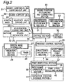
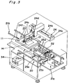
- the printing method according to the above embodiment can be implemented by a printing apparatus according to one embodiment of the present invention as shown in Figs. 2 and 3. More concrete operation of the printing method executed by this printing apparatus is shown in the flowchart of Fig. 4.
- a board carrying-in and carrying-out unit 21 provided with a carrying-in unit 21a and a carrying-out unit 21b, a board support unit 22, a screen mask 11, a squeegee head driving unit 24, a stage section 20 provided with an XY ⁇ -position correcting unit 25 and a stencil separation unit 26, and a screen mask heating unit 27 provided with an induction heating section 28 and a timer 29 can be respectively driven under control of a control section 34.
- the control section 34 receives the inputs of board position recognition correction information from a board position recognizing and correcting section 30 provided with a processing operation section 31 and a recognition camera section 32 as well as print inspection information from a print inspecting section 38 provided with a processing operation section 39, a print state detecting means 40, and an inspection criteria storage section 41.
- the control section 34 inputs process information to and outputs process information from a process control section 35 provided with a processing operation section 36 and an acceptable product print database 37 and receives the input of information of the print state from the print inspecting section 38, thereby executing process control.
- the control section 34 displays the results of operation and inspection, the state of the printed solder paste 12, and so forth on a display section 33 as the occasion demands.
- the board 14 is carried in to the stage section 20 by the carrying-in unit 21a of the board carrying-in and carrying-out unit 21, corrected in position in the stage section 20, thereafter moved to a printing position, printed in the printing position, and thereafter carried out of the printing apparatus from the printing position by the carrying-out unit 21b of the board carrying-in and carrying-out unit 21.
- the board 14 is retained in position by the board support unit 22 provided in the stage section 20.
- the board 14 is retained in position by, for example, a method for vacuum-sucking the board 14 with a number of suction holes opened on the surface of the board support unit 22, a method for supporting the lower surface of the board 14 by means of a number of backup pins or the like.
- a position correcting mark(s) (not shown) of the board 14 is recognized by the recognition camera section 32 of the board position recognizing and correcting section 30.
- the processing operation section 31 calculates a positional displacement between the recognized position of the board 14 and the position of the screen mask 11, and calculates the position correction amount of the board 14 for correcting this positional displacement.
- This result of calculation is inputted to the XY ⁇ -position correcting unit 25 of the stage section 20.
- the positional correction of the board 14 relative to the screen mask 11 is executed by the XY ⁇ -position correcting unit 25 of the stage section 20. That is, the XY ⁇ -position correcting unit 25 executes the positional correction of the board 14 in the orthogonal XY-directions along the horizontal plane of the printing apparatus and in a ⁇ -direction around the Z-axis in the vertical direction relative to the screen mask 11 on the basis of the above position correction information.
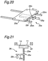
- the XY ⁇ -position correcting unit 25 is constructed so that a Y-direction table 25b capable of moving in the Y-direction is placed on an X-direction table 25a capable of moving in the X-direction (direction in which the board is carried in and out) and a ⁇ -direction table 25c capable of turning in the ⁇ -direction is further placed on them. Then, by moving each of the tables in the respective directions by the position correction amount, the positional correction of the board 14 is executed.
- the positional correction in the X-direction is executed by the X-direction table 25a after the positional correction in the Y-direction and the ⁇ -direction is completed and before the board 14 is brought in contact with the screen mask 11 after the board 14 is moved to the printing position and stopped there.
- FIG. 20 An X-direction driving unit 20x that concurrently serves as this X-direction position correcting unit is shown in Fig. 20.
- the X-direction table 25a is arranged movably in the X-direction along a pair of linear guides 25m extending in the X-direction, and a threaded shaft 25n is rotated forwardly and reversely by driving a driving motor 25p forwardly and reversely, thereby moving forwardly or backwardly the X-direction table 25a fixed to a nut 25r meshed with the threaded shaft 25n in the X-direction.
- the board 14 retained by the board support unit 22 is moved in the X-direction to the printing position by the X-direction driving unit 20x of the stage section 20.
- the board 14 In the printing position, the board 14 is positioned below the screen mask 11 and moved up until the upper surface of the board 14 is brought in contact with the lower surface of the screen mask 11 by the stencil separation unit 26.
- the solder paste 12 is supplied to the one end in the X-direction of the screen mask 11, and the squeegee 13 is moved by the squeegee head driving unit 24 from the one end to the other end in the X-direction of the screen mask 11, thereby filling the solder paste 12 into the through hole 11a of the screen mask 11.
- the screen mask 11 is constructed by forming, opening portions comprised of through holes 11a corresponding to copper-made conductor pattern portions (lands) 15 of the board 14 through, for example, a plate made of nickel or stainless steel having a thickness of about 150 ⁇ m.
- the squeegee head driving unit 24 is to move on the screen mask 11 the squeegee 13 for filling the solder paste 12 into the through holes 11a of the screen mask 11.
- the squeegee 13 is constructed of a flat plate or a plate having a sword-like (roughly pentagonal) cross-section shape.
- the squeegee 13 is moved on the screen mask 11 by forwardly and reversely rotating a ball thread 24b by the driving of a motor 24c and forwardly and backwardly moving a squeegee head 24a meshed with the ball thread 24b in the axial direction of the ball thread 24b.
- the squeegee head 24a can be moved up and down by the forward and reverse rotation of a motor 24d.
- the tilt angle of the squeegee 13 itself relative to the screen mask 11 can also be adjusted by a cylinder 24f. That is, the squeegee 13 is pivotally supported at a portion that is not shown, and by upward or downward moving one end of the squeegee 13 by driving the cylinder 24f, the tilt of the squeegee 13 can be adjusted by pivoting the squeegee 13 around the above support point used as a fulcrum.
- solder paste 12 filled in each of the through holes 11a of the screen mask 11 comes to have a lower end surface put in contact with each of the lands 15 of the board 14 corresponding to the through holes 11a, and by separating the screen mask 11 from the board 14 by the stencil separation unit 26, the solder paste layers 12a are formed on the lands 15 of the board 14.
- FIG. 21 An example of the stencil separation unit 26 is shown in Fig. 21.
- a driving nut 25v is rotated forwardly and reversely via a belt 25u by the forward and reverse rotational driving of an AC servomotor 25t so as to upward or downward move a threaded shaft 25w meshed with the nut 25v, thereby upward or downward moving the board support unit 22 fixed to the upper end of the threaded shaft 25w for the upward or downward movement of the board 14.
- the AC servomotor 25t of the stencil separation unit 26 is driven to move up the board 14 until the upper surface of the board 14 is brought in contact with the lower surface of the screen mask 11.
- the board 14 is moved down relative to the screen mask 11 by the driving of the AC servomotor 25t of the stencil separation unit 26 in order to effect the stencil separation operation.
- the board 14 separated from the stencil is carried out of the printing apparatus by the carrying-out unit 21b.
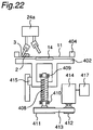
- Fig. 22 shows another stencil separation unit.
- a stage section (board support unit) 402 an AC servo controller 417, an AC servomotor 414 to be controlled by the AC servo controller 417, a ball thread 408 to be rotated forwardly and reversely by an AC servomotor 414, an upper bearing 409 of the ball thread 408, a lower bearing 410 of the ball thread 408, a pulley 411 on the ball thread 408 side, a pulley 412 on the AC servomotor 414 side, a timing belt 413, and a linear guide 415 that guides the upward and downward movement of the stage section 402.
- This stencil separation unit is constructed so that the stage section (board support unit) 402 can move up and down at an arbitrarily set velocity within an arbitrarily set range by the AC servo controller 417, the AC servomotor 414 and the ball thread 408, whereby the stencil separation velocity of the board 14 with respect to the screen mask 11 can be arbitrarily adjusted.
- the screen mask 11 is heated by induction heating by the screen mask heating unit 27.
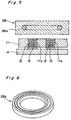
- a ring-shaped induction coil 28a of the induction heating section 28 is arranged in a state in which the coil is separated apart by a specified distance above the screen mask 11.
- an electric current is made to flow through the induction coil 28a for a time set by the timer 29, that is, for example, a time within several milliseconds to several seconds so as to generate an induction magnetic field and flow an induction current through the screen mask 11 itself, thereby directly heating the screen mask 11 itself by the induction heating.
- the induction heating is executed by supplying an electric power of 1400 W for several seconds at 100 V and 60 Hz.
- the induction coil 28a is arranged a specified interval apart from the upper surface of the screen mask 11 in a noncontact manner as shown in Fig. 5. It is acceptable to retreat the coil from above the screen mask 11 during the printing of the solder paste 12 so as not to hinder the printing of the solder paste 12 and move the coil to the place above the screen mask 11 during the induction heating so as to allow the induction heating to be effected. It is preferred that the interval between the induction coil 28a and the screen mask 11 is arranged to a dimension such that a specified current flows through the screen mask 11 by the induction coil 28a.
- the screen mask 11 is made of a conductive material such as stainless steel.
- the stainless steel or the like has a greater resistance than copper, and therefore, the screen mask itself generates heat.
- the solder paste 12 which has a small solder particle diameter or a cream-like form due to the flux, exhibits no electric conductivity, so that no induction current flows to generate no heat. Therefore, as shown in Fig. 7, if the screen mask 11 is heated by the induction heating, then the temperatures of the inner wall surfaces of the through holes 11a of the screen mask 11 are increased. Therefore, the temperature increases in the portion which belongs to the solder paste 12 and is put in contact with the inner wall surface of each through hole 11a and around the portion.
- the temperature does not increase in the center portion of the solder paste 12, so that a temperature gradient as shown in Fig. 7B is formed between the center portion of the solder paste 12 and the peripheral portion (the portion in contact with the through hole 11a). That is, the solder paste 12 comes to have a temperature gradient such that the portion put in contact with the inner wall surface of the through hole 11a has a high temperature and the temperature gradually reduces from the portion toward the center portion of the solder paste 12. Consequently, as shown in Fig. 7A, the viscosity of the solder paste 12 reduces in the peripheral portion than in the center portion. This is because the solder paste 12 has a characteristic as shown in Fig.
- the viscosity of the solder paste 12 becomes reduced between the inner wall surface of the through hole 11a of the screen mask 11 and the solder paste 12 put in contact with the inner wall surface, for which the solder paste 12 is easy to separate from the through hole 11a of the screen mask 11, meaning that the stencil separation is satisfactorily achieved.
- the material of the solder paste 12 should preferably include 90 percent by weight of metal powder and 10 percent by weight of flux.
- the metal powder contains about 62 percent by weight of tin and the other component of lead, and its particle diameter is 20 to 40 ⁇ m.
- the flux has a solvent of 75 to 40 percent by weight of alcohol and the like and 25 to 60 percent by weight of other solid components.
- the solid components include rosin, activator, and thixotropic agent.
- As a concrete product name of the solder paste there can be enumerated the solder paste of a product number MR7125 having 63 percent by weight of tin and 37 percent by weight of lead, produced by Panasonic.
- a stainless-steel-based metal e.g., SUS304
- nickel-chrome system e.g., nickel-chrome system etc.
- nickel-based metal or the like e.g., nickel-based metal or the like.
- a screen mask constructed by forming a conductive vapor-deposited film or a plating film on the surface of a synthetic resin such as polyimide and the inner wall surface of the through hole. In this case, an electromagnetic induction can be generated in the portion of the conductive vapor-deposited film or the plating film on the inner wall surface of the through hole.
- the board 14 that serves as the object on which a print is to be formed is constructed of copper having an excellent conductivity, then no heat is generated in the board 14 by the electromagnetic induction, causing no bad influence on the electronic components and so forth on the board.
- the print inspecting section 38 measures the state in which the solder paste layer 12a is formed on the land 15 of the board 14, i.e., the shape and position of the solder paste layer 12a by means of a camera or a laser length measuring instrument as an example of the print state detecting means 40, and the volume and the amount of positional displacement of the solder paste layer 12a are calculated by the processing operation section 39 on the basis of the results of measurement.
- the laser length measuring instrument applies a laser beam to the solder paste layer 12a and calculates the height and so on of the solder paste layer 12a from the position of reflection light. The above results of calculation are compared with the inspection criteria stored in the inspection criteria storage section 41, and it is decided whether the print is good or not.
- the result of decision is outputted to the control section 34, and if the print is defective, the contents of the defect are numerically expressed and the numeric value is also outputted to the control section 34.
- This deciding operation is executed by, for example, calculating the height, width, volume and so on of the solder paste layer 12a from, for example, an image captured by the camera of the print state detecting means 40 or position data measured by the laser length measuring instrument, comparing the decision data of the height, width, volume and so on of the solder paste layer stored in the inspection criteria storage section 41 with the above calculated values in the processing operation section 39, and deciding whether the print is good or not.
- the process control section 35 changes the parameter setting of the printing apparatus on the basis of the post-printing data of the state in which the solder paste 12 is printed, made by the print inspecting section 38.
- the above parameters include, for example, the parameters of each unit stored in the acceptable product print database 37 (for example, printing velocity, tilt angle of the squeegee 13, environmental temperature during printing (for example, squeegee temperature, screen mask temperature, board temperature, and temperature of air and the like around them, enumerated in the order of importance), printing pressure, i.e., pressure of the squeegee 13 pressed against the screen mask 11, stencil separation velocity of the board 14, and profile of acceleration) and induction heating conditions (for example, heating output, heating time, and heating start timing).
- Relations between the parameters and the print quality are stored as database, and the optimum parameters are calculated by the processing operation section 36 of the process control section 35.
- step S1 the screen mask 11 is carried in to the stage section 20 by the carrying-in unit 21a of the board carrying-in and carrying-out unit 21.
- step S2 the board 14 carried in to the stage section 20 is supported by the board support unit 22.
- step S3 the board position recognizing and correcting section 30 recognizes the position of the board 14 retained by the board support unit 22 and calculates the position correction amount of the board 14 relative to the screen mask 11.
- step S4 the positions in the XY ⁇ -directions of the board 14 relative to the screen mask 11 are each corrected by the XY ⁇ -position correcting unit 25 of the stage section 20 on the basis of the above calculated position correction amount.
- step S5 the board 14 is positioned in the printing position below the screen mask 11 by the stage section 20, and the board 14 is moved up by the stage section 20 so that the screen mask 11 comes in contact with the upper surface of the board 14.
- step S6 the squeegee 13 is moved on the screen mask 11, thereby filling the solder paste 12 into the through holes 11a of the screen mask 11.
- step S7 it is decided whether or not the screen mask 11 is to be inductively heated.
- the program flow proceeds to step S8.
- the program flow proceeds to step S9 to set the timer 29 to a predetermined heating time.
- the screen mask 11 is inductively heated by the induction coil 28a of the induction heating section 28.
- the stencil separation operation is executed in step S8 immediately after the execution of the induction heating. That is, by driving the stencil separation unit 26 of the stage section 20, the board 14 is moved down relative to the screen mask 11 to separate the board 14 from the screen mask 11 and transfer the solder paste 12 from inside the through holes 11a of the screen mask 11 onto the lands 15 of the board 14.
- the above stencil separation operation is executed after the completion of the printing of the solder paste 12, thereby transferring the solder paste 12 from inside the through holes 11a of the screen mask 11 onto the lands 15 of the board 14.
- step S12 the shapes, positions and so on of the solder paste layers 12a formed on the board 14 are inspected by the print inspecting section 38.
- step S13 it is decided whether the print state is good or not as the result of the above inspection.
- the program flow proceeds to step S14 to carry the board 14 out of the printing apparatus by the carrying-out unit 21b in step S14, and the sequence of printing operations ends.
- the program flow proceeds to step S15 to change the design of the process parameter(s) by the process control section 35 and end the sequence of printing operations.
- the next printing of the solder paste 12 is executed on the basis of the optimum condition information obtained through the design change in step S15, and the post-printing stencil separation process in step S8 and the induction heating process of the screen mask 11 in step S10 are executed.
- the screen mask 11 itself is heated by the induction heating, so that the outer peripheral portion of the solder paste 12 put in contact with the inner wall surface of each of the through holes 11a of the screen mask 11 comes to have a temperature increased more than that in the center portion, consequently acquiring a reduced viscosity.
- the adhesive force between the inner wall surface of the through hole 11a of the screen mask 11 and the solder paste 12 is reduced, so that the solder paste 12 easily separates from the screen mask 11, thereby allowing the stencil separation operation to be satisfactorily achieved.
- solder paste 12 is not left on the screen mask 11 side causing no blur of print in the next printing stage, so that a specified amount of solder paste 12 can be supplied, that is, the solder paste 12 can be supplied in the specified shape to the specified position, thereby allowing the solder paste layer(s) 12a to be formed as a print.
- the screen mask 11 itself generates heat, so that the heat discharge of the screen mask 11 can be performed immediately after the stop of the induction heating operation.
- the members other than the screen mask 11 are not heated, so that no bad influence is exerted on the next printing operation, the peripheral units around the screen mask 11 and so on.
- the method of merely radiating heat from the outside of the screen mask 11 to heat the screen mask 11 as observed in the case of hot air, radiation heating (infrared heating), or conduction heating the members and air around the screen mask 11 are heated, and the members and air around the heating unit is heated due to the heating of the heating unit itself.
- the induction coil 28a of the induction heating section 28 does not come in contact with the solder paste 12 left on the surface of the screen mask 11, and therefore, the induction coil 28a is not smeared by the solder paste 12.
- this noncontact method when there is an electronic component(s) on the lower surface of the board 14, the distance to the electronic component is increased, so that the possible exertion of bad influence on the electronic component during the induction heating can be prevented.
- the shearing force of the solder paste 12 filled in the through hole 11a of the screen mask 11 at the time of separation from the stencil exhibits no reduction in shearing force in the portion of a through hole pitch of not greater than 0.2 mm.
- a pitch of 0.2 mm is the limit of the fine printing and no significant reduction in shearing force could be expected when a distance d from the inner wall surface of the through hole was not greater than 0.05 mm.
- the fine printing at a pitch of 0.3 mm which has been difficult, conventionally can be satisfactorily performed, and fine printing can also be performed to the extent of a pitch of about 0.2 mm depending on the conditions of the solder paste and so on.
- the temperature of the screen mask 11 can be increased to about 50 to 70°C with interposition of a gap of 1 mm. Furthermore, by setting the supply power to about 2000 W, the equivalent temperature increase can be achieved within one second, whereby the solder paste inside the through hole 11a is allowed to achieve a greater temperature difference between the inner wall surface of the through hole 11a and the center portion thereof. By putting the induction coil in contact with the screen mask 11, a more efficient temperature increase can be achieved.
- the temperature difference between the inner wall surface of the through hole 11a and the center portion of the through hole 11a depends on the through hole width. Therefore, according to the screen mask having a plurality of types of through hole widths, it is preferable that the condition setting is performed in accordance with the minimum through hole size among the plurality of through holes to be subjected to the induction heating. That is, if the minimum through hole width is about 0.15 mm, then, as described above, then there is necessitated such a sharp control as the supply of a power of 2000 W to the induction coil for a supply time of about one second.
- the heating conditions of the induction coil can be preparatorily determined according to the pattern of the screen mask (i.e., the arrangement, size and so on of the through holes).
- the induction coil heating conditions conforming to the through hole size may be set to the heating conditions close to the optimum characteristic values appropriate for the separation from the stencil of each through hole obtained from the previously-measured characteristic values (viscosity, shearing stress value and yield value with respect to temperature) of the solder paste.
- the temperature control can also be executed by induction heating when executing the mask cleaning of the screen mask 11.
- the solder paste left inside the through hole and the rear surface of the screen mask can be more efficiently removed.
- the conditions in the case are not required to be controlled strictly as compared with the time of separation from the stencil, and the screen mask is required to be heated to such an extent that the solder paste comes to have a good flowability.
- the heating may be executed with, for example, a power of 1000 W during the cleaning time.
- the board 14 is moved down in the state in which the screen mask 11 is made stationary in order to separate the screen mask 11 from the board 14 relative to each other.
- the present invention is not limited to this, and the screen mask 11 may be moved in a state in which the board 14 is made stationary. It is also acceptable to move both the screen mask 11 and the board 14 in directions in which they are separated from each other.
- the printing paste is not limited to the solder paste 12, and any arbitrary material may be used so long as the present invention can be applied.
- the material may be constructed of a metal powder having a minute particle diameter of not greater than about 200 ⁇ m and a flux instead of the solder paste.
- this metal powder there can be enumerated silver or copper.
- the induction heating is effected after the completion of the printing paste scraping operation by the squeegee.
- the present invention is not limited to this, and it is acceptable to start the induction heating simultaneously with the scraping operation, execute the heating at a temperature lower than the specified heating temperature in the initial stage and increase the temperature of the outer peripheral portion of the printing paste to the above specified temperature by the induction heating after the completion of the scraping operation for the reduction in viscosity of the paste.
- the present invention is not limited to the uniform induction heating of the whole body of the screen mask 11, and it is acceptable to make the induction coil 28a partially face the portion in which the separation of the solder paste 12 from the stencil is unsatisfactory among the circuit pattern, and inductively heat only the portion.
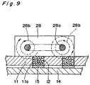
- the present invention is not limited to the noncontact induction heating, and as shown in Fig. 9, it is acceptable to inductively heat the induction heating section 28 in contact with the upper surface of the screen mask 11. In this case, the distance between the induction coil 28a of the induction heating section 28 and the screen mask 11 reduces, and therefore, the induction heating can be efficiently effected in a locally concentrated manner.
- the reference numeral 28b in Fig. 9 denotes an induction magnetic field.
- the through hole 11a elongated in the Y-direction it is also preferable for the through hole 11a elongated in the Y-direction to arrange an induction coil 28c in the lengthwise direction of the hole 11a and generate an induction current by flowing a current through the induction coil as indicated by the line denoted by 28c in Fig. 10B.
- the induction coil is arranged in the direction of arrow 28e and flow an induction current through the induction coil, then the inner wall surface of the through hole 11a along the Y-direction generates heat not so much.
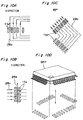
- a QFP Quad Flat Package
- the lengthwise directions of the through holes 11a of adjacent sides cross each other at an angle of 45 degrees.
- the identical induction heating section can flow a current through the induction coil only in the X-direction, flow a current through the induction coil only in the Y-direction, or flow a current through the induction coils alternately in the X-direction and the Y-direction, so that the general-purpose properties of the induction heating section can be improved.
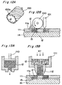
- Fig. 12A and Fig. 12B show an embodiment of the present invention according to the screen printing system, in which a filling roller 100 for filling the solder paste 12 is used instead of the squeegee.
- the cylindrical filling roller 100 is rotated to hold printing material, e.g., the solder paste 12 and forcibly fill the solder paste 12 into the through holes 11a of the screen mask 11.
- the cylindrical shape of the filling roller 100 may alternately be the sawtooth-shaped one having spiral grooves 100a shown in Fig. 12A.
- the reference numeral 101 denotes a solder paste-scraping-use scraper in Fig. 12A.
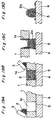
- a print material 112 such as solder paste into the through holes 11a of the screen mask 11 by means of a nozzle 111 having an extruding function of a piston 110 as shown in Fig. 13A or an extruding function of compressed air as shown in Fig. 13B.
- the reference numeral 112 denotes a solder paste-scraping-use scraper provided at the tip of the nozzle 111.
- the present invention can also be applied not only to the screen printing but also to other printing methods.
- Fig. 14 shows an embodiment in which the present invention is applied to a direct-printing planographic transfer printing system.
- a print material 122 supplied in a specified pattern on a flat plate 120 is directly transferred to a specified position 115 of a board 114 that is the object on which a print is to be formed.
- the adhesive force between the flat plate 120 and the print material 122 is reduced by inductively heating a surface on which the print material 122 is in close contact with the flat plate 120, thereby producing an effect of facilitating the emigration of the print material to the specified position 115 of the object 114 on which a print is to be formed.
- Fig. 15A and Fig. 15B show an embodiment in which the present invention is applied to an offset printing system.
- a print material 142 is supplied from a tank 139 stored with the print material 142 to recess portions 136a of a plate cylinder 136 by three rollers 140, thereby transferring the print material 142 inside the recess portions 136a onto a rubber cylinder 137.
- the print material 142 on the rubber cylinder 137 is transferred and printed on a paper 135 that serves as the object which is to be put between the rubber cylinder 137 and an impression cylinder 138 and on which a print is to be formed.
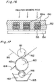
- Fig. 16 shows an embodiment in which the present invention is applied to a planographic intaglio transfer printing system.
- this embodiment by increasing the temperature of an intaglio 150 itself through inductively heating the intaglio 150 similar to the screen printing system, there can be obtained the effect that the shearing force of the print material such as solder paste 152 on the inner wall surface of each of recess portions 150a is reduced and the transferability to specified positions 155 such as lands of a board 154 is improved.
- Fig. 17 shows an embodiment in which the present invention is applied to an intaglio transfer printing system (gravure printing system).
- a print material such as solder paste 162 inside a tank 165 is supplied to recess portions 163a of a plate cylinder 163 by a supply roller 166, and the print material 162 in the recess portions 163a is transferred and printed onto a base material 160 held between the plate cylinder 163 and an impression cylinder 161.
- the reference numeral 164 denotes a doctor, and this doctor 164 scrapes off an excessive amount of print material 162 of the print material 162 filled into the recess portions 163a.
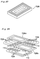
- Fig. 23 shows a perspective view of an induction coil according to another embodiment of the present invention.
- the induction coil is not limited to the annular one, and the induction coil may be a square-frame-shaped or a rectangular-frame-shaped induction coil 728.
- Fig. 24 is a perspective view showing a state in which two units 728a and 728b of the induction coil 728 of Fig. 23 are prepared and arranged at two corners located in diagonal positions of a board on which a QFP is to be positioned and an induction current 729 is flowed in the lengthwise direction of each through hole 11a.
- the two induction coils 728a and 728b are preferably operated simultaneously.
- Fig. 25 is a perspective view showing a state in which four units 728c, 728d, 728e, and 728f of the induction coil 728 of Fig. 23 are prepared and arranged at the four corners of a board on which a QFP is to be positioned and an induction current 729 is flowed in the lengthwise direction of each through hole 11a.
- the four induction coils 728c through 728f are also operated simultaneously.
- Fig. 26 is a perspective view showing a state in which one induction coil 728g of Fig. 23 is prepared and arranged above a board portion on which a QFP is to be positioned and one side edge of the induction coil 728g is arranged in a form inclined at an angle of 45 degrees with respect to the direction in which the through holes 11a are arranged, so that an equal amount of induction current 729 flows through each through hole 11a.
Landscapes
- Engineering & Computer Science (AREA)
- Mechanical Engineering (AREA)
- Manufacturing & Machinery (AREA)
- Microelectronics & Electronic Packaging (AREA)
- Electric Connection Of Electric Components To Printed Circuits (AREA)
- Screen Printers (AREA)
- Printing Methods (AREA)
- Inking, Control Or Cleaning Of Printing Machines (AREA)
Applications Claiming Priority (3)
| Application Number | Priority Date | Filing Date | Title |
|---|---|---|---|
| JP123393/96 | 1996-05-17 | ||
| JP12339396 | 1996-05-17 | ||
| PCT/JP1997/001650 WO1997044191A1 (fr) | 1996-05-17 | 1997-05-16 | Technique d'impression et appareil d'impression |
Publications (2)
| Publication Number | Publication Date |
|---|---|
| EP0904938A1 true EP0904938A1 (fr) | 1999-03-31 |
| EP0904938A4 EP0904938A4 (fr) | 2002-08-14 |
Family
ID=14859461
Family Applications (1)
| Application Number | Title | Priority Date | Filing Date |
|---|---|---|---|
| EP97922072A Withdrawn EP0904938A4 (fr) | 1996-05-17 | 1997-05-16 | Technique d'impression et appareil d'impression |
Country Status (4)
| Country | Link |
|---|---|
| US (2) | US6230619B1 (fr) |
| EP (1) | EP0904938A4 (fr) |
| KR (1) | KR100308635B1 (fr) |
| WO (1) | WO1997044191A1 (fr) |
Cited By (1)
| Publication number | Priority date | Publication date | Assignee | Title |
|---|---|---|---|---|
| EP1705029A1 (fr) | 2005-03-22 | 2006-09-27 | Koenen Gmbh | Pochoir pour serigraphie |
Families Citing this family (26)
| Publication number | Priority date | Publication date | Assignee | Title |
|---|---|---|---|---|
| US6352025B1 (en) * | 2000-09-01 | 2002-03-05 | Motorola, Inc. | Solder printing apparatus |
| JP4239403B2 (ja) * | 2000-12-06 | 2009-03-18 | ソニー株式会社 | 光ディスク |
| US20040163553A1 (en) * | 2001-10-19 | 2004-08-26 | Tom Bock | Frame preparation for screen printing |
| CH695817A5 (de) * | 2002-08-16 | 2006-08-31 | Inducs Ag | Bratgerät. |
| BR0204183A (pt) * | 2002-09-23 | 2004-06-01 | Ian Royce William Pet Conzalez | Processo e dispositivo para a aplicação de camadas adesivas curáveis por radiação |
| KR100945348B1 (ko) * | 2002-12-27 | 2010-03-08 | 엘지디스플레이 주식회사 | 액정 표시 소자의 액정층 형성 방법 |
| KR100950134B1 (ko) * | 2002-12-27 | 2010-03-30 | 엘지디스플레이 주식회사 | 레지스트인쇄용 클리체 및 그 제조방법 |
| KR100950133B1 (ko) * | 2002-12-27 | 2010-03-30 | 엘지디스플레이 주식회사 | 인쇄방식에 의한 패턴형성방법 |
| US6871776B2 (en) * | 2003-03-10 | 2005-03-29 | Trucco Horacio Andres | Manufacture of solid-solder-deposit PCB utilizing electrically heated wire mesh |
| US7121647B2 (en) * | 2003-10-03 | 2006-10-17 | Lexmark International, Inc. | Method of applying an encapsulant material to an ink jet printhead |
| US7895247B2 (en) | 2003-10-29 | 2011-02-22 | Oracle International Corporation | Tracking space usage in a database |
| TW200540681A (en) * | 2004-06-15 | 2005-12-16 | Four Tech Co Ltd A | Winding method for mouse pad with induction coil |
| US7404613B2 (en) * | 2004-06-30 | 2008-07-29 | Lexmark International, Inc. | Inkjet print cartridge having an adhesive with improved dimensional control |
| US7331503B2 (en) * | 2004-10-29 | 2008-02-19 | Intel Corporation | Solder printing process to reduce void formation in a microvia |
| JP4379348B2 (ja) * | 2005-02-15 | 2009-12-09 | パナソニック株式会社 | 電子部品実装システムおよび電子部品実装方法 |
| US7861650B2 (en) * | 2007-04-13 | 2011-01-04 | Illinois Tool Works, Inc. | Method and apparatus for adjusting a substrate support |
| US20090095176A1 (en) * | 2007-10-11 | 2009-04-16 | Printar Ltd. | Method and apparatus for PCB finishing processes |
| KR20090081472A (ko) * | 2008-01-24 | 2009-07-29 | 삼성전자주식회사 | 실장 기판 및 이를 이용한 반도체 패키지의 제조 방법 |
| JP5043764B2 (ja) * | 2008-06-30 | 2012-10-10 | 株式会社ジャパンユニックス | レーザー式はんだ付け方法及び装置 |
| TW201002528A (en) * | 2008-07-02 | 2010-01-16 | Atma Champ Entpr Corp | Contactless screen printing method and equipment thereof |
| JP5881237B2 (ja) * | 2011-10-28 | 2016-03-09 | Jukiオートメーションシステムズ株式会社 | 検査装置、処理装置、情報処理装置、対象物製造装置及びその製造方法 |
| JP6446736B2 (ja) * | 2014-07-14 | 2019-01-09 | 株式会社ブイ・テクノロジー | 成膜方法及び成膜装置 |
| CN106227946B (zh) * | 2016-07-26 | 2019-03-12 | 上海望友信息科技有限公司 | 一种pcb网板制作方法及系统 |
| US20190247944A1 (en) * | 2018-02-11 | 2019-08-15 | Powertech Technology Inc. | Flux transfer method |
| US20230060880A1 (en) * | 2021-08-24 | 2023-03-02 | Robert Bosch Gmbh | Flattening surface of pasted track in stencil printing process |
| EP4611493B1 (fr) * | 2024-02-29 | 2026-02-11 | Siemens Aktiengesellschaft | Procédé de surveillance de la disponibilité de pression d'un masque d'impression, programme informatique et système informatique |
Family Cites Families (9)
| Publication number | Priority date | Publication date | Assignee | Title |
|---|---|---|---|---|
| US3656428A (en) * | 1970-06-15 | 1972-04-18 | Gen Motors Corp | Method of screen printing |
| US4050269A (en) * | 1974-04-29 | 1977-09-27 | Ciba-Geigy Ag | Dry thermal transfer of organic compounds by needle-bearing support |
| GB2050946B (en) * | 1979-05-30 | 1983-02-16 | Tdk Electronics Co Ltd | Hot melt screen printing machine and process for producing a screen printing plate |
| US4911948A (en) * | 1988-09-07 | 1990-03-27 | Acumeter Laboratories, Inc. | Method of screen printing and application of hot melt upon moving web substrates |
| JP2870905B2 (ja) * | 1989-12-25 | 1999-03-17 | 松下電器産業株式会社 | スクリーン印刷方法および装置 |
| JP2720572B2 (ja) | 1990-05-07 | 1998-03-04 | 松下電器産業株式会社 | クリーム半田印刷方法 |
| JPH04223137A (ja) * | 1990-12-26 | 1992-08-13 | Dainippon Ink & Chem Inc | 膜体類の接着方法、接着装置及び接着材料 |
| JP3193448B2 (ja) | 1992-04-17 | 2001-07-30 | 株式会社アイホー | 撹拌機 |
| JP3288128B2 (ja) * | 1993-05-21 | 2002-06-04 | 松下電器産業株式会社 | 印刷装置および印刷方法 |
-
1997
- 1997-05-16 EP EP97922072A patent/EP0904938A4/fr not_active Withdrawn
- 1997-05-16 WO PCT/JP1997/001650 patent/WO1997044191A1/fr not_active Ceased
- 1997-05-16 US US09/180,784 patent/US6230619B1/en not_active Expired - Fee Related
- 1997-05-16 KR KR1019980708957A patent/KR100308635B1/ko not_active Expired - Fee Related
-
2000
- 2000-11-09 US US09/708,415 patent/US6371017B1/en not_active Expired - Fee Related
Cited By (1)
| Publication number | Priority date | Publication date | Assignee | Title |
|---|---|---|---|---|
| EP1705029A1 (fr) | 2005-03-22 | 2006-09-27 | Koenen Gmbh | Pochoir pour serigraphie |
Also Published As
| Publication number | Publication date |
|---|---|
| KR20000010821A (ko) | 2000-02-25 |
| US6371017B1 (en) | 2002-04-16 |
| WO1997044191A1 (fr) | 1997-11-27 |
| KR100308635B1 (ko) | 2001-12-17 |
| US6230619B1 (en) | 2001-05-15 |
| EP0904938A4 (fr) | 2002-08-14 |
Similar Documents
| Publication | Publication Date | Title |
|---|---|---|
| US6230619B1 (en) | Printing method and printing apparatus | |
| EP1448032B1 (fr) | Procédé et installation de sérigraphie | |
| EP0337149A2 (fr) | Outil de déposition de soudure | |
| CN110352635B (zh) | 部件安装系统及粘接剂检查装置 | |
| CN113784534A (zh) | 一种断路修复方法和断路修复装置 | |
| EP0740495A2 (fr) | Procédé et dispositif pour imprimer la pâte à souder | |
| EP1314342B1 (fr) | Procede et dispositif d'application de milieux visqueux sur un substrat, et utilisation de ces procede et dispositif | |
| JP3863980B2 (ja) | 印刷方法及び印刷装置 | |
| EP3986096B1 (fr) | Procédé de mise en forme et dispositif de mise en forme | |
| JP3549705B2 (ja) | 印刷方法及び印刷装置 | |
| US20230014796A1 (en) | Screen mask inspection device, solder printing inspection device, and method for inspecting screen mask | |
| JP3279761B2 (ja) | クリーム半田印刷用マスク及びそれを用いた印刷方法 | |
| EP4122706A1 (fr) | Procédé de moulage | |
| JP2003211631A (ja) | ステンシル印刷方法及びその装置 | |
| JPH08197712A (ja) | クリームはんだ供給方法及びクリームはんだ供給用ス キージ | |
| JP2004096042A (ja) | 回路基板上への接続材料の供給方法及び供給装置 | |
| Morris et al. | Stencil printing of solder paste for fine‐pitch surface mount assembly | |
| CN115484753B (zh) | 用于在smt贴片过程中的电子元件检测方法 | |
| JP4696945B2 (ja) | 配線基板修正方法及び配線基板修正装置 | |
| JP2004241574A (ja) | 電子部品のリペア装置及びリペア方法 | |
| JP2003324271A (ja) | はんだ付け方法 | |
| JP2000071422A (ja) | スキージ及びスクリーン印刷装置並びにスクリーン印刷方法 | |
| KR20120111308A (ko) | 스크린 프린터 | |
| CN118921881A (zh) | 一种柔性电路板的制备方法及柔性电路板 | |
| JPH05267838A (ja) | 微少量半田供給方法およびその装置 |
Legal Events
| Date | Code | Title | Description |
|---|---|---|---|
| PUAI | Public reference made under article 153(3) epc to a published international application that has entered the european phase |
Free format text: ORIGINAL CODE: 0009012 |
|
| 17P | Request for examination filed |
Effective date: 19981217 |
|
| AK | Designated contracting states |
Kind code of ref document: A1 Designated state(s): DE GB |
|
| A4 | Supplementary search report drawn up and despatched |
Effective date: 20020628 |
|
| AK | Designated contracting states |
Kind code of ref document: A4 Designated state(s): DE GB |
|
| 17Q | First examination report despatched |
Effective date: 20040119 |
|
| GRAP | Despatch of communication of intention to grant a patent |
Free format text: ORIGINAL CODE: EPIDOSNIGR1 |
|
| STAA | Information on the status of an ep patent application or granted ep patent |
Free format text: STATUS: THE APPLICATION IS DEEMED TO BE WITHDRAWN |
|
| 18D | Application deemed to be withdrawn |
Effective date: 20070612 |