EP0905583B1 - Reinigerlose Bilderzeugungsmethode - Google Patents
Reinigerlose Bilderzeugungsmethode Download PDFInfo
- Publication number
- EP0905583B1 EP0905583B1 EP98118387A EP98118387A EP0905583B1 EP 0905583 B1 EP0905583 B1 EP 0905583B1 EP 98118387 A EP98118387 A EP 98118387A EP 98118387 A EP98118387 A EP 98118387A EP 0905583 B1 EP0905583 B1 EP 0905583B1
- Authority
- EP
- European Patent Office
- Prior art keywords
- toner
- developing
- image
- charging
- developer
- Prior art date
- Legal status (The legal status is an assumption and is not a legal conclusion. Google has not performed a legal analysis and makes no representation as to the accuracy of the status listed.)
- Expired - Lifetime
Links
- 238000000034 method Methods 0.000 title claims description 44
- 239000006249 magnetic particle Substances 0.000 claims description 46
- 239000002245 particle Substances 0.000 claims description 44
- 239000010410 layer Substances 0.000 claims description 39
- 239000000463 material Substances 0.000 claims description 38
- 230000008859 change Effects 0.000 claims description 25
- 230000035699 permeability Effects 0.000 claims description 14
- 239000011347 resin Substances 0.000 claims description 14
- 229920005989 resin Polymers 0.000 claims description 14
- 238000004140 cleaning Methods 0.000 claims description 12
- 239000002344 surface layer Substances 0.000 claims description 7
- 230000002159 abnormal effect Effects 0.000 claims description 5
- 238000012546 transfer Methods 0.000 description 47
- 238000011161 development Methods 0.000 description 27
- 230000018109 developmental process Effects 0.000 description 27
- 230000007423 decrease Effects 0.000 description 22
- 230000008569 process Effects 0.000 description 17
- 238000002347 injection Methods 0.000 description 14
- 239000007924 injection Substances 0.000 description 14
- 230000015572 biosynthetic process Effects 0.000 description 12
- 238000005755 formation reaction Methods 0.000 description 12
- 238000009826 distribution Methods 0.000 description 7
- 238000004519 manufacturing process Methods 0.000 description 7
- 239000013589 supplement Substances 0.000 description 7
- 230000002093 peripheral effect Effects 0.000 description 6
- 230000005415 magnetization Effects 0.000 description 5
- 239000007787 solid Substances 0.000 description 5
- 238000003756 stirring Methods 0.000 description 5
- FAPWRFPIFSIZLT-UHFFFAOYSA-M Sodium chloride Chemical compound [Na+].[Cl-] FAPWRFPIFSIZLT-UHFFFAOYSA-M 0.000 description 4
- 229910052782 aluminium Inorganic materials 0.000 description 4
- XAGFODPZIPBFFR-UHFFFAOYSA-N aluminium Chemical compound [Al] XAGFODPZIPBFFR-UHFFFAOYSA-N 0.000 description 4
- 230000008901 benefit Effects 0.000 description 4
- 238000001514 detection method Methods 0.000 description 4
- 239000011521 glass Substances 0.000 description 4
- 230000033001 locomotion Effects 0.000 description 4
- XOLBLPGZBRYERU-UHFFFAOYSA-N tin dioxide Chemical compound O=[Sn]=O XOLBLPGZBRYERU-UHFFFAOYSA-N 0.000 description 4
- CBENFWSGALASAD-UHFFFAOYSA-N Ozone Chemical compound [O-][O+]=O CBENFWSGALASAD-UHFFFAOYSA-N 0.000 description 3
- 229910021417 amorphous silicon Inorganic materials 0.000 description 3
- 238000000576 coating method Methods 0.000 description 3
- 230000003247 decreasing effect Effects 0.000 description 3
- 238000007599 discharging Methods 0.000 description 3
- 230000005684 electric field Effects 0.000 description 3
- 239000008151 electrolyte solution Substances 0.000 description 3
- 230000006870 function Effects 0.000 description 3
- SZVJSHCCFOBDDC-UHFFFAOYSA-N iron(II,III) oxide Inorganic materials O=[Fe]O[Fe]O[Fe]=O SZVJSHCCFOBDDC-UHFFFAOYSA-N 0.000 description 3
- 238000002156 mixing Methods 0.000 description 3
- 230000001105 regulatory effect Effects 0.000 description 3
- 229910000859 α-Fe Inorganic materials 0.000 description 3
- 230000002411 adverse Effects 0.000 description 2
- -1 alkylbenzene sulfonate Chemical class 0.000 description 2
- 238000006243 chemical reaction Methods 0.000 description 2
- 229920001971 elastomer Polymers 0.000 description 2
- 239000010419 fine particle Substances 0.000 description 2
- 239000007788 liquid Substances 0.000 description 2
- 238000005259 measurement Methods 0.000 description 2
- 229910052751 metal Inorganic materials 0.000 description 2
- 239000002184 metal Substances 0.000 description 2
- 239000000203 mixture Substances 0.000 description 2
- 230000003287 optical effect Effects 0.000 description 2
- 229920005668 polycarbonate resin Polymers 0.000 description 2
- 239000004431 polycarbonate resin Substances 0.000 description 2
- 229920001721 polyimide Polymers 0.000 description 2
- 239000009719 polyimide resin Substances 0.000 description 2
- 239000000047 product Substances 0.000 description 2
- 238000004064 recycling Methods 0.000 description 2
- 230000009467 reduction Effects 0.000 description 2
- 239000004065 semiconductor Substances 0.000 description 2
- 239000011780 sodium chloride Substances 0.000 description 2
- PXGOKWXKJXAPGV-UHFFFAOYSA-N Fluorine Chemical compound FF PXGOKWXKJXAPGV-UHFFFAOYSA-N 0.000 description 1
- 239000004677 Nylon Substances 0.000 description 1
- 239000002033 PVDF binder Substances 0.000 description 1
- 239000004696 Poly ether ether ketone Substances 0.000 description 1
- 239000004695 Polyether sulfone Substances 0.000 description 1
- GWEVSGVZZGPLCZ-UHFFFAOYSA-N Titan oxide Chemical compound O=[Ti]=O GWEVSGVZZGPLCZ-UHFFFAOYSA-N 0.000 description 1
- 229910052787 antimony Inorganic materials 0.000 description 1
- WATWJIUSRGPENY-UHFFFAOYSA-N antimony atom Chemical compound [Sb] WATWJIUSRGPENY-UHFFFAOYSA-N 0.000 description 1
- 239000011230 binding agent Substances 0.000 description 1
- 230000033228 biological regulation Effects 0.000 description 1
- 230000005540 biological transmission Effects 0.000 description 1
- 239000006229 carbon black Substances 0.000 description 1
- 239000011248 coating agent Substances 0.000 description 1
- 239000011247 coating layer Substances 0.000 description 1
- 230000001276 controlling effect Effects 0.000 description 1
- 230000007547 defect Effects 0.000 description 1
- 230000002950 deficient Effects 0.000 description 1
- 230000001419 dependent effect Effects 0.000 description 1
- 230000008021 deposition Effects 0.000 description 1
- 230000002542 deteriorative effect Effects 0.000 description 1
- 238000010586 diagram Methods 0.000 description 1
- 125000000664 diazo group Chemical group [N-]=[N+]=[*] 0.000 description 1
- 238000003618 dip coating Methods 0.000 description 1
- 239000002270 dispersing agent Substances 0.000 description 1
- 230000000694 effects Effects 0.000 description 1
- 230000005685 electric field effect Effects 0.000 description 1
- 230000005183 environmental health Effects 0.000 description 1
- 238000002474 experimental method Methods 0.000 description 1
- 239000000835 fiber Substances 0.000 description 1
- 239000000945 filler Substances 0.000 description 1
- 239000012530 fluid Substances 0.000 description 1
- 229910052731 fluorine Inorganic materials 0.000 description 1
- 239000011737 fluorine Substances 0.000 description 1
- 150000007857 hydrazones Chemical class 0.000 description 1
- 238000005286 illumination Methods 0.000 description 1
- 238000009413 insulation Methods 0.000 description 1
- 239000004973 liquid crystal related substance Substances 0.000 description 1
- 239000000696 magnetic material Substances 0.000 description 1
- 238000012423 maintenance Methods 0.000 description 1
- 125000004184 methoxymethyl group Chemical group [H]C([H])([H])OC([H])([H])* 0.000 description 1
- 238000012986 modification Methods 0.000 description 1
- 230000004048 modification Effects 0.000 description 1
- 229920001778 nylon Polymers 0.000 description 1
- 239000000049 pigment Substances 0.000 description 1
- 239000000088 plastic resin Substances 0.000 description 1
- 229920003207 poly(ethylene-2,6-naphthalate) Polymers 0.000 description 1
- 229920006122 polyamide resin Polymers 0.000 description 1
- 229920006393 polyether sulfone Polymers 0.000 description 1
- 229920002530 polyetherether ketone Polymers 0.000 description 1
- 239000011112 polyethylene naphthalate Substances 0.000 description 1
- 239000005020 polyethylene terephthalate Substances 0.000 description 1
- 229920000139 polyethylene terephthalate Polymers 0.000 description 1
- 229920005749 polyurethane resin Polymers 0.000 description 1
- 229920002981 polyvinylidene fluoride Polymers 0.000 description 1
- 238000003825 pressing Methods 0.000 description 1
- 238000012545 processing Methods 0.000 description 1
- 230000001737 promoting effect Effects 0.000 description 1
- 230000001846 repelling effect Effects 0.000 description 1
- 230000004044 response Effects 0.000 description 1
- 230000000630 rising effect Effects 0.000 description 1
- 238000007761 roller coating Methods 0.000 description 1
- 238000000926 separation method Methods 0.000 description 1
- 229920002379 silicone rubber Polymers 0.000 description 1
- 238000005549 size reduction Methods 0.000 description 1
- 239000000243 solution Substances 0.000 description 1
- 238000005507 spraying Methods 0.000 description 1
- 239000004094 surface-active agent Substances 0.000 description 1
- OGIDPMRJRNCKJF-UHFFFAOYSA-N titanium oxide Inorganic materials [Ti]=O OGIDPMRJRNCKJF-UHFFFAOYSA-N 0.000 description 1
- 239000011882 ultra-fine particle Substances 0.000 description 1
- XLYOFNOQVPJJNP-UHFFFAOYSA-N water Substances O XLYOFNOQVPJJNP-UHFFFAOYSA-N 0.000 description 1
Images
Classifications
-
- G—PHYSICS
- G03—PHOTOGRAPHY; CINEMATOGRAPHY; ANALOGOUS TECHNIQUES USING WAVES OTHER THAN OPTICAL WAVES; ELECTROGRAPHY; HOLOGRAPHY
- G03G—ELECTROGRAPHY; ELECTROPHOTOGRAPHY; MAGNETOGRAPHY
- G03G15/00—Apparatus for electrographic processes using a charge pattern
- G03G15/02—Apparatus for electrographic processes using a charge pattern for laying down a uniform charge, e.g. for sensitising; Corona discharge devices
- G03G15/0208—Apparatus for electrographic processes using a charge pattern for laying down a uniform charge, e.g. for sensitising; Corona discharge devices by contact, friction or induction, e.g. liquid charging apparatus
- G03G15/0241—Apparatus for electrographic processes using a charge pattern for laying down a uniform charge, e.g. for sensitising; Corona discharge devices by contact, friction or induction, e.g. liquid charging apparatus by bringing charging powder particles into contact with the member to be charged, e.g. by means of a magnetic brush
-
- G—PHYSICS
- G03—PHOTOGRAPHY; CINEMATOGRAPHY; ANALOGOUS TECHNIQUES USING WAVES OTHER THAN OPTICAL WAVES; ELECTROGRAPHY; HOLOGRAPHY
- G03G—ELECTROGRAPHY; ELECTROPHOTOGRAPHY; MAGNETOGRAPHY
- G03G15/00—Apparatus for electrographic processes using a charge pattern
- G03G15/06—Apparatus for electrographic processes using a charge pattern for developing
- G03G15/08—Apparatus for electrographic processes using a charge pattern for developing using a solid developer, e.g. powder developer
- G03G15/0822—Arrangements for preparing, mixing, supplying or dispensing developer
- G03G15/0848—Arrangements for testing or measuring developer properties or quality, e.g. charge, size, flowability
- G03G15/0849—Detection or control means for the developer concentration
- G03G15/0853—Detection or control means for the developer concentration the concentration being measured by magnetic means
-
- G—PHYSICS
- G03—PHOTOGRAPHY; CINEMATOGRAPHY; ANALOGOUS TECHNIQUES USING WAVES OTHER THAN OPTICAL WAVES; ELECTROGRAPHY; HOLOGRAPHY
- G03G—ELECTROGRAPHY; ELECTROPHOTOGRAPHY; MAGNETOGRAPHY
- G03G21/00—Arrangements not provided for by groups G03G13/00 - G03G19/00, e.g. cleaning, elimination of residual charge
- G03G21/0005—Arrangements not provided for by groups G03G13/00 - G03G19/00, e.g. cleaning, elimination of residual charge for removing solid developer or debris from the electrographic recording medium
- G03G21/0064—Arrangements not provided for by groups G03G13/00 - G03G19/00, e.g. cleaning, elimination of residual charge for removing solid developer or debris from the electrographic recording medium using the developing unit, e.g. cleanerless or multi-cycle apparatus
-
- G—PHYSICS
- G03—PHOTOGRAPHY; CINEMATOGRAPHY; ANALOGOUS TECHNIQUES USING WAVES OTHER THAN OPTICAL WAVES; ELECTROGRAPHY; HOLOGRAPHY
- G03G—ELECTROGRAPHY; ELECTROPHOTOGRAPHY; MAGNETOGRAPHY
- G03G2215/00—Apparatus for electrophotographic processes
- G03G2215/02—Arrangements for laying down a uniform charge
- G03G2215/021—Arrangements for laying down a uniform charge by contact, friction or induction
- G03G2215/022—Arrangements for laying down a uniform charge by contact, friction or induction using a magnetic brush
-
- G—PHYSICS
- G03—PHOTOGRAPHY; CINEMATOGRAPHY; ANALOGOUS TECHNIQUES USING WAVES OTHER THAN OPTICAL WAVES; ELECTROGRAPHY; HOLOGRAPHY
- G03G—ELECTROGRAPHY; ELECTROPHOTOGRAPHY; MAGNETOGRAPHY
- G03G2221/00—Processes not provided for by group G03G2215/00, e.g. cleaning or residual charge elimination
- G03G2221/0005—Cleaning of residual toner
Definitions
- the present invention relates to an image forming method for an image forming apparatus having a magnetic brush charger contactable to an image bearing member to charge an image bearing member.
- a transfer type image forming apparatus has been widely used wherein an image is formed by image forming process means including a charging means for charging a member to be charged(image bearing member) such as an electrophotographic photosensitive member or a dielectric member for electrostatic recording, image information writing means for forming an electrostatic latent image on the charged surface of the member to be charged, developing means for forming a toner image by developing an electrostatic latent image with a developer and transferring means for transferring a toner image on a transfer material, and wherein the toner image is transferred onto a transfer material, and the transferred image is fixed to provide a print (copy, print or the like), and the member to be charged is repeatedly used.
- image forming process means including a charging means for charging a member to be charged(image bearing member) such as an electrophotographic photosensitive member or a dielectric member for electrostatic recording, image information writing means for forming an electrostatic latent image on the charged surface of the member to be charged, developing means for forming a toner image by developing an electrostatic la
- a corona charger As the charging means for charging the member to be charged to a predetermined polarity and potential, a corona charger has been widely used.
- a corona charger is disposed faced to the photosensitive drum without contact thereto, so that photosensitive drum surface is exposed to the corona emitted from the corona charger to charge the photosensitive drum surface to a predetermined polarity and potential.
- a contact charging type charging device (contact charging device) is put into practice since it is advantageous in the low ozone production, low electric power consumption or the like as compared with the non-contact type.
- a contact charging member supplied with a voltage is contacted to the photosensitive drum, so that photosensitive drum surface is charged to a predetermined polarity and potential.
- electroconductive magnetic particles are magnetically confined on a carrying member, and magnetic brush portion of a magnetic brush charging member is contacted to the member to be charged, wherein the charging member is applied with a bias voltage, by which the member to be charged is charged, and it is preferably used from the standpoint of stability of the charging contact.
- the magnetic brush charging member electroconductive magnetic particles are directly confined on a magnet as a carrying member or magnetically confined on a sleeve enclosing a magnet, so that magnetic brush portion is formed, and is contacted to the member to be charged with or without rotation, and the charging is started by application of the voltage.
- electroconductive fibers may be formed into a brush (furbrush member), or an electroconductive rubber is formed into a roller (electroconductive rubber roller(charging roller)).
- the charged potential of the surface of the member to be charged is substantially equivalent to the DC component of the bias application to the contact charging member(Japanese Laid-open Patent Application No. HEI-6-3921).
- injection charging Charging of the member to be charged by direct injection of the charge at the contact portion.
- the injection charging does not use the discharge phenomenon which has been used in the corona charger, so that complete ozoneless charging can be accomplished together with the low electric power consumption, and therefore, it is noted.
- the developing means for forming a toner image by development of an electrostatic latent image with a developer is classified generally into 4 types.
- the toner in the developer is gradually consumed with development for the electrostatic latent image, and if the toner supplement is not carried out, the toner content of the developer (mixing ratio of the toner particle and the magnetic carrier, T/C ratio) gradually decreases with the result that image density decreases, too.
- a means is provided to detect the toner content of the developer in the developing device, and on the basis of the toner content detected information, the toner is supplied from the supplement portion into the developing device corresponding to the toner consumed by the development, by which the T/C ratio of the developer is maintained in a predetermined range (developer density control system).
- Untransferred toner on the member to be charged after the transfer is collected by a cleaning means(cleaner) and is disposed of finally.
- the residual toner is preferably not produced.
- the small amount of the toner remaining on the member to be charged after the transfer is removed by fog removing bias (a fog removing potential difference Vback which is a potential difference between the surface potential of the member to be charged and the DC voltage applied to the developing means) in the subsequent developing operation or operations.
- fog removing bias a fog removing potential difference Vback which is a potential difference between the surface potential of the member to be charged and the DC voltage applied to the developing means
- Vback a fog removing potential difference
- the toner particles remaining on the member to be charged after the toner image transfer onto the transfer material are carried over to the charge station for the member to be charged, and is temporarily collected into the magnetic brush portion of a magnetic brush charging member in a magnetic brush contact charging device, and the toner particles thus temporarily collected are gradually ejected to the member to be charged by electrostatic force from the magnetic brush portion, so that it is carried on the member to be charged to the developing station where it is removed by the simultaneous development and cleaning.
- the toner particles have relatively high electric resistance, and therefore, the introduction of the toner particles in the magnetic brush portion of the magnetic brush charging member, increases the resistance of the magnetic brush portion so that charging power is decreased.
- the operations are in good order, since the amount of the untransferred toner introduced in the magnetic brush portion is small, since the toner is ejected to the member to be charged, and since the tolerable amount in the magnetic brush portion is relatively large.
- the toner particles discharged onto the member to be charged from the magnetic brush portion are very uniformly distributed thereon, and the amount thereof is very small, and therefore, they do not adversely affect the image exposure process. Additionally, the production of the ghost image attributable to the untransferred toner pattern can be prevented.
- the mixing toner content in the magnetic brush portion suddenly increases. If the amount thereof exceeds the tolerable level, the ejection of the toner from the magnetic brush portion becomes not enough with the result of decrease of the Charging power due to the rise of the resistance of the magnetic brush portion, and therefore, the potential difference between the potential of the member to be charged and the potential applied to the magnetic brush charging member becomes so large that magnetic particles constituting the magnetic brush portion are deposited on the member to be charged from the magnetic brush portion, abnormally.
- the magnetic particles removed from the magnetic brush portion are carried over to the developing station and are collected thereby, in the cleaner-less system.
- the charged potential Due to the decrease of the charging power attributable to the decrease of the magnetic particles from the magnetic brush portion (improper charging, charging non-uniformity or the like), the charged potential thereby does not reach to the predetermined potential, and due to the decrease of the charged potential of the member to be charged, the magnetic particle disengagement phenomenon is promoted. As a result, image defect may occur.
- Document EP-A-0 844 536 describes an image forming method executed by an image forming apparatus as defined above.
- Document EP-A 0 580 014 describes an image recording apparatus comprising a toner concentration detecting circuit for detecting a toner concentration of two-component developer composed of toner and carrier by detecting a change of magnetic permeability of the two-component developer, for use in a developing device of the image recording apparatus.
- the toner concentration detecting circuit includes a sensor by which a change of magnetic permeability of the two-component developer is detected, a waveform corrector, a counter connected to a control CPU and a gate signal generating circuit connected to the control CPU by which a gate signal is sent to the counter.
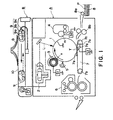
- Figure 1 is a schematic view of an example of an image forming apparatus according to an embodiment of the present invention.
- the image forming apparatus is shown as a laser beam printer of an image transfer type electrophotographic process type, magnetic brush contact charging type and cleaner-less system type.
- Designated by A is a laser beam printer, and B is an image reader or scanner for reading an image, placed on the printer.
- an original supporting platen glass fixed on an upper surface of the apparatus, and on the original supporting platen glass an original G is placed face down thereon, and an unshown original cover is covered thereon.
- Designated by 9 is an image reading unit (reader portion) an original illumination lamp 9a, a short focus lens array 9b, CCD sensor 9c and the like.
- the unit 9 upon actuation of an unshown copy key, is moved forward along a bottom surface of the glass from its home position at the right-hand portion, and upon arrival at a predetermined forward movement end portion, it is moved backward to the home position.
- the image surface of the set original G on the original supporting platen glass 10 is illuminated and scanned from the right-hand side to the left-hand side by the original projection lamp 9a of the unit 9, and the light reflected by the surface of the original is imaged on a CCD sensor 9c by the short focus lens array 9b.
- the CCD sensor 9c comprises a light receiving portion, a transfer portion and an output portion.
- a light signal is converted to a charge signal by the light receiving CCD portion, and the charge signal is transferred to an output portion in synchronization with clock pulses by a transfer portion.
- the charge signal is converted to a voltage signal, which is then amplified with impedance reduction treatment, and the resultant signal is outputted.
- the analog signal provided in this manner is subjected to a known image processing, so that digital signal is produced and is fed to the printer A.
- the image reading device B carries out photoelectric reading of the image information of the original G and conversion thereof to a time series electrical digital pixel signal(image signal).
- a printer A designated by 1 is an electrophotographic photosensitive member(photosensitive drum) of a rotatable drum type as a member to be charged.
- the photosensitive member of this example is a negative chargeable OPC photosensitive member having a surface charge injection layer.
- the photosensitive member 1 will be described in detail hereinafter (2).
- the photosensitive drum 1 is rotated about a center thereof in the clockwise direction indicated by an arrow at a predetermined peripheral speed, at rotational speed of 100mm/sec in this example, and in the rotation process it is subjected to a whole surface pre-exposure by the pre-exposure device(eraser lamp) 5 so that electrical memory in the previous image formation process is erased, and then it is charged uniformly to the negative in the example by the charging means 3.
- the charging means 3 is a magnetic brush contact charging device.
- the charging device 2 will be described in detail hereinafter(3).
- the thus charged surface of the photosensitive member 1 is exposed to and scanned by a laser scanner 2 having an intensity modulated in accordance with image signal fed to the printer A from the image reading device B, corresponding to the intended image information, so that electrostatic latent image thereof is formed in accordance with the image signal.
- the laser scanner 2 includes a start light signal generator, s solid laser element, a collimator lens system, a rotatable polygonal mirror (polygonal mirror).
- the solid laser element When the rotatable photosensitive drum surface is subjected to the laser scanning exposure L by the laser scanner 2, the solid laser element is rendered on and off at predetermined timing ((ON/OFF) by start light signal generator in response to the inputted image signal.
- the laser beam emitted from the solid laser element is converted into afocal beam through a collimator lens system, and is then deflected by a rotatable polygonal mirror which is rotating at high speed, and then is focus on the photosensitive drum surface 1 as a spot by a f ⁇ lens group.
- an exposure distribution of one scan of the image is formed on the photosensitive drum surface 1, and the photosensitive drum surface is scrolled in the perpendicular direction by the rotation of the photosensitive drum 1 after each scan, so that exposure distribution corresponding to the image signal is provided on the rotatable photosensitive drum surface.
- the formed electrostatic latent image on the surface of the rotatable photosensitive drum 1 is developed sequentially into a toner image by the developing device 4.
- a reverse development system is used.
- the developing device 4 is a magnetic brush developing device of a two-component contact type developing system. The developing device 4 will be described in detail hereinafter(5).
- a recording material (transfer material) P accommodated in a sheet feeding cassette 8 is, fed out by sheet feeding rollers 8a one by one, and is fed into the printer A. It is fed to the transfer portion T in the form of a contact nip between the photosensitive drum 1 and a transfer belt 6 as a transferring means at a predetermined controlled timing by registration rollers 8b.
- the toner image is electrostatically transferred onto the surface of the transfer material P fed to the transfer portion T, from the surface of the rotating photosensitive drum by a transfer charging blade 7 d disposed inside the transfer belt 7.
- the transferring device 7 will be described in detail hereinafter (5).
- the transfer material P now having the transferred toner image at the transfer portion 75 is sequentially separated from the surface of the photosensitive drum 1, and is fed by an extension of f transfer belt type transferring device 7 to a fixing device 6 where the toner image is heat fixed thereon, and then is discharged onto the sheet discharge tray 8 as a copy or print.
- the image forming apparatus of this example is not provided with a cleaning device (cleaner) exclusively for removing the residual toner from the surface of the rotatable photosensitive drum 1 after the toner image transfer, and the developing device 4 has a function of collection or removing the residual toner from the surface of the photosensitive drum 1, namely, the developing device 4 functions also as a cleaning means (cleaner-less system).
- the rotatable photosensitive drum 1 is used for the repeated image formation.
- the cleaner-less system will be described in detail in (6) hereinafter.
- the photosensitive drum 1 as the member to be charged may be an organic photosensitive member or the like which is normally used.
- Other usable members are photosensitive members using CdS, Si, Se or another inorganic semiconductor. Desirably, it has a surface layer of a material having a volume resistivity of 10 9 -10 14 ⁇ cm on an organic photosensitive member, or it is an amorphous silicon photosensitive member, since the charge injection charging can be used with the advantages of low ozone production and low electric power consumption. The charging property may also be improved.
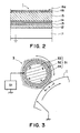
- the photosensitive drum 1 used in this example is a negatively chargeable organic photosensitive member having a surface charge injection layer, and comprises a drum base(aluminum base) of aluminum having a diameter of 30mm, and following first to fifth layers thereon.
- Figure 2 is a schematic view of the layers.
- First layer 12 primer layer in the form of an electroconductive layer having a thickness of 20 ⁇ m, provided to uniform the aluminum base 11.
- Second layer 13 positive charge injection preventing layer in the form of intermediate resistance layer having a thickness of 1 ⁇ m and having a volume resistivity of approx. 1x 10 6 ⁇ cm adjusted by AMILAN (tradename of polyamide resin material, available from Toray Kabushiki Kaisha, Japan) resin material and methoxymethyl nylon, provided to prevent cancellation of the negative charge on the photosensitive member surface by the positive charge injected from the aluminum base 11.
- AMILAN tradename of polyamide resin material, available from Toray Kabushiki Kaisha, Japan
- Third layer 14 charge generating layer of resin material in which disazo pigment is dispersed, having a thickness of approx.0.3 ⁇ m. This layer generates a couple of positive and negative charges upon exposure to light.
- Fourth layer 15 charge transfer layer of polycarbonate resin material in which hydrazone is dispersed.
- This layer is a P-type semiconductor. Therefore, the negative charge on the photosensitive member surface cannot move through this layer, and only the positive charge generated in the charge generating layer can be transferred onto the photosensitive member surface.
- Fifth layer 16 is a charge injection layer and is a coating layer of an insulative resin material binder in which electroconductive fine particles and SnO 2 ultra-fine particles 16 are dispersed. More particularly, it comprises insulative resin material and 70 % by weight, on the basis of the resin material, of SnO 2 particles having a particle size of 0.03 ⁇ m which are doped with light transmissive electroconductive filler of antimony to reduce the resistance (electroconductive).
- Such coating liquid is applied into a thickness of approx. 3 ⁇ m through a proper coating method such as dip coating method, spray coating method, roller coating method, beam coating method or the like, thus providing a charge injection layer.
- a proper coating method such as dip coating method, spray coating method, roller coating method, beam coating method or the like, thus providing a charge injection layer.
- the surface resistance thereof is 10 13 ⁇ cm. By controlling the surface resistance in such a manner, the direct charging property is improved to permit high quality image formation.
- the photosensitive member is not limited to an OPC material, but may be of an a-Si material, and a further increase of durability is possible.
- the volume resistivity of the surface layer is measured in this manner.
- Metal electrodes are distributed at the clearance of 200 ⁇ m, and liquid surface layer material is supplied therebetween, and is formed into a film, and then, 100V is applied between the electrodes.
- the measuring temperature is 23°C, and the humidity is 50%RH.
- the charging device 3 is a magnetic brush contact charging device.
- Figure 3 is a schematic illustration.
- Designated by 31 is a magnetic brush charging member as a contact charging member contacted to the photosensitive drum 1.
- the magnetic brush charging member 31 of this example is of a rotatable sleeve type comprising a non-rotatable magnet roller 33, a non-magnetic sleeve (non-magnetic, electroconductive electrode sleeve) 32 fitted rotatably around the magnet roller coaxially therewith, having an outer diameter of 16mm, and a magnetic brush portion 34 of electroconductive magnetic particle (charging magnetic particles) attracted on the outer surface of the non-magnetic sleeve 32 by the magnetic force of the magnet roller 33 therein.
- the magnetic brush charging member 31 is disposed substantially parallel with the photosensitive drum 1 with the magnetic brush portion 34 contacted to the surface of the photosensitive drum 1.
- the contact nip (charge portion) width n provided between the photosensitive drum 1 and the magnetic brush portion 34 is adjusted to be approx. 5mm.
- the charging magnetic particles for constituting the magnetic brush portion 34 preferably have:
- the resistance is not less than 1x 10 6 ⁇ cm.
- the magnetic particles preferably have:
- the resistance value of the magnetic particles is measured in the following manner: 2g of the magnetic particles is placed in a metal cell having a bottom surface area of 228mm 2 to which a voltage is applied, and the current is measured when a voltage of 100V is applied.
- the average particle size of the magnetic particles is indicated by a maximum angular distance in the horizontal direction. More than 300 particles are randomly extracted using an optical microscope, and diameters thereof are measured, and the measurements are averaged.
- a automatic DC magnetization B-H property recording device BHH-50 available from Riken Denshi Kabushiki Kaisha, is usable.
- the particles are filled into a cylindrical container having a diameter(inner diameter)6.5mm and height 10mm, at approx. 2g, and motion of the particles in the container is prevented.
- the saturation magnetization is measured from the B-H curve.
- the magnetic particle may be, for example, a resin material carrier comprising a resin material in which magnetite is dispersed as a magnetic material and in which carbon black is dispersed for electroconductivity and for resistance adjustment, or magnetite alone such as ferrite or the like having an oxidized or deoxidized surface for resistance adjustment, or magnetite alone such as ferrite or the like having a surface coated with resin material for resistance adjustment.
- a resin material carrier comprising a resin material in which magnetite is dispersed as a magnetic material and in which carbon black is dispersed for electroconductivity and for resistance adjustment, or magnetite alone such as ferrite or the like having an oxidized or deoxidized surface for resistance adjustment, or magnetite alone such as ferrite or the like having a surface coated with resin material for resistance adjustment.
- the use is made with ferrite a surface of which is subjected to an oxide or deoxidization process to adjust the resistance.
- the non-magnetic sleeve 32 of the magnetic brush charging member 31 is rotated at 150mm/sec (the peripheral speed of the photosensitive drum 1 is 100mm/sec) in the counterclockwise direction indicated by an arrow, namely, in the opposite peripheral direction (counter unidirectional) relative to the surface moving direction of the photosensitive drum 1 in the charging region n.
- the non-magnetic sleeve 32 is application with a predetermined charging bias from a charging bias applying voltage source S1.
- the charging condition is a constant voltage controlled DC bias voltage of -550V.
- the magnetic brush portion 34 With rotation of the non-magnetic sleeve 32, the magnetic brush portion 34 rotates in the same direction as the sleeve 32, and in the charging region n it rubs the surface of the photosensitive drum 1, so that electric charge is given to the photosensitive drum 1 from the charging magnetic particle constituting the magnetic brush portion 34, and thus uniformly charging the surface of the photosensitive drum 1 to a predetermined polarity and potential (contact charging).
- the photosensitive drum 1 is provided with a charge injection layer 16 at its surface, and therefore, the photosensitive drum 1 is charged through charge injection charging.
- a predetermined charging bias voltage to the non-magnetic sleeve 32, the charge is given to the photosensitive drum 1 from the magnetic particles constituting the magnetic brush portion 34, by which the surface of the photosensitive drum 1 is charged to a potential corresponding to the charging bias voltage.
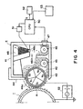
- Figure 4 shows a schematic structure of a developing device 4 used in this example.
- the developing device 4 uses as a developer a mixture of non-magnetic toner particles and magnetic carrier particles (magnetic carrier for development), and the developer is formed into a magnetic brush layer by magnetic force on the developer carrying member. It is carried to the developing zone (developing zone) of the photosensitive drum 1, and the magnetic brush is contacted to the surface of the photosensitive drum 1 to develop the electrostatic latent image into a toner image (two component magnetic brush contact developing system).
- Designated by 41 is a developing container; 42 is a developing sleeve as the developer carrying member; 43 is a magnet roller as a magnetic field generating means stationarily fixed in the developing sleeve 42; 44 is a developer layer thickness regulating blade for forming a thin layer of the developer on developing sleeve surface; 45 is a developer stirring and feeding screw; 46 is the two component developer accommodated in the developing container 41, which comprises non-magnetic toner particles t and magnetic carrier particles c mixed therewith.
- the two component developer used in this embodiment comprises:
- the toner and carrier were mixed at weight ratio of 6: 94.
- the triboelectric charge amount of the toner in the developer was approx. 25x 10 -3 c/kg.
- the volume average particle size of the toner is determined, for example, in the following manner.
- a measuring apparatus is a Coulter counter TA-II (product of Coulter Co., Ltd.) To this apparatus, an interface (product of NIPPON KAGAKU SEIKI) through which the values of the average diameter distribution and average volume distribution of the toner particles are outputted, and a personal computer (Canon CX-1), are connected.
- the electrolytic solution is 1 % water solution of NaCl (first class sodium chloride).
- surfactant which is desirably constituted of alkylbenzene sulfonate, is added as dispersant in 100 - 150 ml of the aforementioned electrolytic solution, and then, 0.5 - 50 mg of the toner particles are added.
- the electrolytic solution in which the toner particles are suspended is processed approximately 1 - 3 minutes by an ultrasonic dispersing device. Then, the distribution of the toner particles measuring 2 - 40 microns in particle size is measured with the use of the aforementioned Coulter counter TA-2, the aperture of which is set at 100 microns, and the volumetric distribution of the toner particles is obtained. Finally, the volumetric average particle size of the toner particles is calculated from the thus obtained volumetric distribution of the toner particles.
- the developing sleeve 42 is so disposed that at least at the time of the developing operation, it is placed with the closest distance from the photosensitive drum 1 being approx. 500 ⁇ m, So that magnetic developer brush thin layer 46a on the outer surface of the developing sleeve 42 is contacted to the surface of the photosensitive drum 1.
- the contact nip m between the magnetic developer brush layer 46a and the photosensitive drum 1 is a developing zone.
- the developing sleeve 42 is rotated around the stationary magnet roller 43 in the counterclockwise direction indicated by the arrow at a predetermined rotational speed.
- a magnetic brush of the developer 46 is formed on the outer surface of the sleeve by the magnetic force of the magnet roller 43.
- the magnetic developer brush is fed with the rotation of the sleeve 42, and is subjected to layer thickness regulation by the blade 44 so as to be a magnetic developer brush thin layer 46a having a predetermined layer thickness, and is carried out of the developing container to the developing zone. It is contacted to the surface of the photosensitive drum 1, and is returned into the developing container 41 by the continuing rotation of the sleeve 42.
- the developer 46 With the rotation of the developing sleeve 42, the developer 46 is taken by the N2 pole of the magnet roller 43, and is conveyed by the S2 pole - N1 pole, during which it is regulated by the regulating blade 44 disposed perpendicularly relative to the developing sleeve 42, so that thin layer 46a of the developer 46 is formed on the developing sleeve 42.
- the developer layer 46a thus formed in the thin layer is fed to the position of the main developing pole S 1 in the developing zone, where it is reformed as chains of developer by the magnetic force.
- the electrostatic latent image on the photosensitive drum 1 is developed into a toner image, and thereafter, by the repelling magnetic field formed between the thereafter N 3 pole and the N 2 pole, the developer on the developing sleeve 42 is returned into the developing container 41.
- a developing bias in the form of a DC voltage plus alternating voltage is applied from a developing bias applying voltage source S2.
- the developing bias voltage is as follows:
- the application of the alternating voltage is effective to increase the development efficiency so that image quality is improved in the two-component developer type developing method, but the fog tends to be produced. Therefore, a potential difference is provided between the DC voltage applied normally to the developing sleeve 42 and the surface potential (dark portion potential) of the photosensitive drum 1, by which the fog production is prevented.
- the potential difference for removing the fog is called a fog removing potential (Vback), by which the deposition of the toner on the photosensitive drum 1 at the non-image region is prevented during the developing operation.
- the toner in the developer is gradually consumed for the development of the electrostatic latent image, and if the toner supplement is not effected, the toner content in the developer (T/C ratio (ratio of the toner amount relative to the amount of the carrier)) gradually decreases, and the image density of the output image is decreased. Therefore, a sensor 47 for detecting the toner content in the developer 46 in the developing container 41 is provided, and the amount of the toner t is supplied into the developer 46 from the supplement portion 48 corresponding to the toner consumed by the development on the basis of the toner content detected information detected by the sensor 47, by which the T/C ratio in the developer 46 is kept in a predetermined constant range (developer density control system).
- T/C ratio ratio of the toner amount relative to the amount of the carrier
- the toner content detecting sensor 47 uses a magnetic permeability change of the developer, and detects the apparent magnetic permeability ⁇ of the magnetic carrier included in the developer in a predetermined volume of the developer adjacent the sensor using the inductance of the coil.
- the sensor 47 per se is known.
- the magnetic permeability information of the developer 46 outputted from the sensor 47 during the developing device operation, is supplied to the control circuit (CPU) 50, which detects the T/C ratio of the developer 46 in the developing container on the basis of the input information.
- the event means that T/C ratio of the developer 46 is decreased (low toner content), and when the toner content of the decrease decreases, the event means that T/C ratio of the developer 46 increases (high toner content).
- a toner supply shaft 48a of a toner supplement portion 48 is driven through a driver 51, so that toner supply is started from the toner supplement portion 48 to the developer 46 in the developing container. Supplied toner is introduced to and dispersed in the developer 46 by stirring screws 45, 45.
- the control circuit 50 determines the T/C ratio of the developer 46 in the developing container.
- the control circuit 50 stops driving of the toner supply shaft 48a of the toner supplement portion 48 through a driver 51, thus terminating the toner supply.
- T/C the ratio of the developer 46 in the developing container is controlled and maintained in a predetermined range of the developer toner content.
- the position of the sensor 47 it is provided on a side wall surface of the developer stirring chamber in the developing container 41 in this embodiment, but it may be placed at another place if there is a sufficient thickness of the developer which on the sensor surface of the toner content detecting sensor 18 so that toner content detection is possible, and if the flow of the developer is constant during the developer stirring, namely, the flow speed of the developer flowing along the sensor surface is constant during the developer stirring, and the fluid is regular.
- the transferring device 7 in this example is in the form of a transfer belt type, as has been mentioned hereinbefore.
- Designated by 7 a ia an endless transfer belt, and is stretched around the driving roller 7 b and the follower roller 7 c, and is rotated substantially at the same peripheral speed as the peripheral speed of the photosensitive drum 1 in the same peripheral moving direction.
- Designated by 7 d is a transfer charging blade disposed inside the transfer belt 7 a, and forms a transfer nip T by pressing the upper portion of the transfer belt 7 a to the photosensitive drum 1, and a transfer bias is applied thereto from a transfer bias application voltage source S3 to charge it to the opposite polarity from the toner at the back side of the transfer material P.
- the belt 7a is of polyimide resin material and has a film thickness of 75 ⁇ m.
- the material of the belt 7a is not limited to polyimide resin material, but may be of polycarbonate resin material, polyethylene terephthalate resin material, polyvinylidene fluoride resin material, polyethylenenaphthalate resin material, polyetheretherketone resin material, polyether sulfone resin material, polyurethane resin material or another plastic resin material, or a fluorine or silicon rubber.
- the thickness it is not limited to 75 ⁇ m, but may range approx. 25-2000 ⁇ m, preferably 50-150 ⁇ m.
- the transfer charging blade 7d has a resistance of 1x 10 5 -1x 10 7 ⁇ , a thickness of 2mm, and a length of 306mm.
- the transfer charging blade 7d is supplied with a bias of +15 ⁇ A under a constant-current-control to effect the image transfer.
- the image forming apparatus of this example is a cleaner-less system (toner recycling system), and therefore, the toner particles remaining on the photosensitive drum 1 after toner image transfer onto the transfer material P (untransferred toner) is carried over to the charge portion n of the photosensitive drum 1 and is introduced to the magnetic brush portion 34 of the magnetic brush charging member 31 of the magnetic brush contact charging device 3, and is temporarily collected.
- toner recycling system toner recycling system
- the untransferred toner on the photosensitive drum 1 may frequently contain positive and negative particles due to the separation discharge or the like during the or the like operation. Such untransferred toner particles reach to the magnetic brush charging member 31, and are introduced in the magnetic brush portion 34.
- the collection of the untransferred toner into the magnetic brush portion 34 of the magnetic brush charging member 31 can be more effectively carried out by oscillating electric field effect between the magnetic brush charging member 31 and the photosensitive drum 1 provided by the application of the AC voltage component to the magnetic brush charging member 31.
- All of the untransferred toner collected by the magnetic brush portion 34 is charged to the negative polarity by the triboelectric charge with the magnetic particles of the magnetic brush, and then is ejected onto the photosensitive drum 1 by the potential difference between the charged potential of the photosensitive drum 1 and the DC component applied to the charging member 31.
- the photosensitive drum 1 With the movement of the toner to the photosensitive drum 1 from the charging member 31, the photosensitive drum 1 is charged, and the photosensitive drum 1 having the remaining toner is exposed to image light by the laser scanner 2 over the remaining toner so that electrostatic latent image is formed.
- the untransferred toner ejected to the photosensitive drum 1 and having the same polarity, is conveyed to the developing zone m, where it is collected into the developing device by the simultaneous development and cleaning with the fog removing electric field. Simultaneously with the formation of the developing electric field which deposits the toner from the developing sleeve 42 to the light portion of the photosensitive drum, a cleaning electric field for collecting the toner onto the developing sleeve 42 from the dark portion of the photosensitive drum is formed.
- the simultaneous collection of the untransferred toner by the developing device 4 is effected simultaneously with the image formation process including the charging, exposure, development and the transfer operations.
- the untransferred toner is reused for the development after it is collected back into the developing device 4, and therefore, the residual toner to be disposed of can be eliminated.
- the advantage regarding the space saving is significant, so that remarkable downsizing of the image forming apparatus is possible.
- the toner particles have a relatively height electric resistance, and therefore, the introduction of the toner particles in the magnetic brush portion 34 of the magnetic brush charging member 31 increases the resistance of the magnetic brush portion 34 and is one of factors of deteriorating the charging power.
- the amount of the untransferred toner introduced in the magnetic brush portion 34 of the magnetic brush charging member 31 by being carried over to the charge portion n is small, and the toner is discharged from the magnetic brush portion 34, and the tolerable amount of the introduced toner is relatively large. Therefore, the introduction is practically not a problem.
- the toner particles ejected to the photosensitive drum 1 from the magnetic brush portion 34 are very uniformly distributed thereon, and therefore, the subsequent image exposure process is not adversely affected, substantially. No ghost image attributable to the untransferred toner pattern is produced.
- the mixing toner content in the magnetic brush portion suddenly increases. If the amount thereof exceeds the tolerable level, the ejection of the toner from the magnetic brush portion becomes not enough. This results decrease of the charging power due to the rise of the resistance of the magnetic brush portion, and therefore, the potential difference between the potential of the member to be charged and the potential applied to the magnetic brush charging member becomes so large that magnetic particles constituting the magnetic brush portion are deposited on the member to be charged from the magnetic brush portion, abnormally.
- the disengagements from the magnetic particle results in the decrease of the charging power (improper charging, charging non-uniformity) so that photosensitive drum 1 is not charged to the desired potential, and the removal of the magnetic particles are further increased, and the defective images results.
- the decrease of the magnetic particles in the magnetic brush portion 34 of the magnetic brush charging member 31 is detected, so that abnormal state is recognized, so that production of a large amount of the improper copies or prints. This will be described in detail.
- the degree of the output change (amount of decrease of the T/C ratio per unit time) of the toner content detecting sensor 47 resulting from such event is larger than the degree of output change in the normal operation in which the toner decreases by the normal development for the electrostatic latent image. Therefore, the large degree of the output change means that large amount disengagement of the magnetic particles from the magnetic brush charging member 31 occurs and are introduced in the developer 46 of the developing device 4, and therefore, the amount of the magnetic particles in the magnetic brush charging member 31 has reduced.
- the degree of the output change of the toner content detecting sensor 47 is compared with a predetermined output change rate by the control circuit (CPU) 50, and if it is larger than the predetermined output change rate, it is discriminated that T/C ratio variation is not due to the toner consumption of the normal electrostatic latent image development, but the abnormal disengagement of the magnetic particles from the magnetic brush charging member 31 occurs, and therefore, the amount of the magnetic particles of the magnetic brush charging member 31 has reduced beyond a tolerable level, and the control circuit (CPU) 50 produces a signal S.
- the signal is used for the warning for promoting the user to exchange the image formation cartridge(process cartridge) containing the magnetic brush charging member or the magnetic brush charging member or for the emergency stop of the image forming apparatus.
- Designated by 52 is a warning displaying means in the form of a lamp, buzzer or the like.
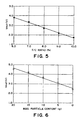
- Figure 5 shows the results of experiments of the inventors, which shows the output Vout(V) of the toner content detecting sensor 47 when T/C the ratio of the developer 46 in the developing device 4 is changed from 6% to 10% by 1%.
- Figure 6 shows the output of the toner content detecting sensor 47 when the charging magnetic particles are forcedly introduced in the developing device 4 containing the developer 46 of the T/C ratio of 8%.
- the toner consumption amount in 1sec when whole surface solid black printing is effected on a transfer material P of A3 size is approx. 0.45g, and the 1sec required for 1% (T/C ratio) of the toner to be consumed with the whole surface solid black printing on A3 size sheet, is approx. 4.5sec.
- the actual detection of the 1% change by the toner content detecting sensor 47 is approx. 20sec after the event because of the distance between the toner content detecting sensor 47 and the developing sleeve 42.
- the time required for the output of the toner content detecting sensor 47 to make the change corresponding to 1 % change of T/C ratio is approx. 5sec in this situation.
- the control circuit 50 recognizes that T/C ratio variation is not by the toner consumption of normal development operation but by the abnormal disengagement of the magnetic particles in the magnetic brush charging member 31 (due to the sheet jam, power failure or forced voltage source off, and a signal indicative of the event is produced.
- the user can be notified of the event that amount of the magnetic particles in the magnetic brush portion 34 of the magnetic brush charging member 31 is reduced beyond a tolerable level, so that wasteful copying operation thereafter can be avoided.
- the image forming apparatus is provided with a video counter 53 ( Figure 4).
- the other structures are the same as with Embodiment 1.
- the image signal is converted to a digital signal by an analog - digital conversion device, and the output level of the converted signal is integrated for each pixel. It is then converted to a video count by a video counter 53 and is then supplied to the control circuit (CPU) 50.
- CPU control circuit
- the control circuit 50 calculates the toner consumption amount on the basis of the video count, and predicts the varying T/C ratio.
- the comparison is made between the changing rate and a change rate of the T/C ratio predicted on the basis of the input from the video counter 53.
- the control circuit 50 recognizes the change of the T/C ratio variation is not by the toner consumption due to the normal developing operation, but by the abnormal disengagement of the magnetic particles from the magnetic brush charging member 31 described above, and the signal indicative of the event is produced.
- the user can be notified of the event that amount of the magnetic particles in the magnetic brush portion 34 of the magnetic brush charging member 31 is reduced beyond a tolerable level, so that wasteful copying operation thereafter can be avoided.
Landscapes
- Physics & Mathematics (AREA)
- General Physics & Mathematics (AREA)
- Engineering & Computer Science (AREA)
- Plasma & Fusion (AREA)
- Electrostatic Charge, Transfer And Separation In Electrography (AREA)
- Dry Development In Electrophotography (AREA)
- Control Or Security For Electrophotography (AREA)
- Magnetic Brush Developing In Electrophotography (AREA)
Claims (10)
- Bilderzeugungsverfahren, welches in einem Bilderzeugungsgerät ausführbar ist, wobei das Gerät enthält:wobei das Verfahren die Schritte enthält:ein bildtragendes Teil (1);ein Aufladungsmittel (3), welches magnetische Partikel enthält, welche an dem bildtragenden Teil kontaktierbar sind; ein Entwicklungsmittel (4) zur Entwicklung, mit einem Entwickler (46), wobei ein elektrostatisches Bild auf dem bildtragenden Teil unter Verwendung eines Aufladungsbetriebes des Aufladungsteils erzeugt wird, wobei das Entwicklungsmittel in der Lage ist, Resttoner von dem bildtragenden Teil aufzusammeln, und der Entwickler einen nichtmagnetischen Toner und magnetischen Träger enthält;gekennzeichnet durch die Schritte:Aufladen des bildtragenden Teils durch Kontaktieren der magnetischen Partikel des Aufladungsmittels auf das bildtragende Teil; undAufsammeln des Resttoners von dem bildtragenden Teil durch das Entwicklungsmittel;Erfassen einer magnetischen Permeabilität des Entwicklers in dem Entwicklungsmittel durch eine Erfassungsvorrichtung (47), welche an dem Entwicklungsmittel bereitgestellt ist;Beurteilen, ob eine Ausgabeänderungsrate der Erfassungsvorrichtung aufgrund der Einführung von magnetischen Partikeln von dem Aufladungsmittel (3) in den Entwickler höher als ein vorbestimmter Wert ist; und wenn dies der Fall istAnzeigen an einen Benutzer über ein Anzeigemittel, dass das Aufladungsmittel (3) in einem abnormalen Zustand ist.
- Verfahren nach Anspruch 1, ferner enthaltend einen Schritt des Zuführens von nichtmagnetischem Toner in die Entwicklungsvorrichtung durch ein Zuführmittel (48), wenn die Ausgabe des Erfassungsmittels nicht geringer als ein vorbestimmtes Limit ist.
- Verfahren nach Anspruch 1, bei welchem das Aufladungsmittel mit einer Spannung versorgt wird.
- Verfahren nach Anspruch 3, bei welchem die Spannung eine überlagerte Spannung aus einer Wechselspannung und einer Gleichspannung ist.
- Verfahren nach Anspruch 1, bei welchem der vorbestimmte Wert auf Basis von Bildinformation zum Erzeugen des elektrostatischen Bildes bestimmt wird.
- Verfahren nach Anspruch 1, bei welchem das bildtragende Teil (1) mit einer Oberflächenschicht (16) bereitgestellt ist, welche einen Durchgangswiderstand von 10-9 bis 10-14 Ω/cm hat.
- Verfahren nach Anspruch 6, bei welchem die Oberflächenschicht Kunstharzmaterial und darin dispergierte elektrisch leitfähige Partikel enthält.
- Verfahren nach Anspruch 6 oder 7, bei welchem das bildtragende Teil mit einer lichtempfindlichen Schicht bereitgestellt ist, welche innerhalb der Oberflächenschicht bereitgestellt ist.
- Verfahren nach Anspruch 1, bei welchem ein Entwicklungsbetrieb zum Entwickeln des elektrostatischen Bildes durch den Entwickler und ein Reinigungsbetrieb zum Aufsammeln des Resttoners von dem bildtragenden Teil gleichzeitig ausgeführt werden.
- Bilderzeugungsgerät mit:wobei das Bilderzeugungsgerät eine Steuerschaltung (50) enthält, welche dazu angepasst ist das Verfahren von jedem der Ansprüche 1 bis 9 auszuführen.einem bildtragenden Teil (1);einem Aufladungsmittel (3), welches magnetische Partikel enthält, welche an dem bildtragenden Teil kontaktierbar sind; einem Entwicklungsmittel (4) zum Entwickeln, mit einem Entwickler (46), wobei unter Verwendung eines Aufladungsbetriebes des Aufladungsmittels ein elektrostatisches Bild auf dem bildtragenden Teil erzeugt wird, wobei das Entwicklungsmittel in der Lage ist Resttoner von dem bildtragenden Teil aufzusammeln, und der Entwickler einen nichtmagnetischen Toner und magnetischen Träger enthält;einer Erfassungsvorrichtung (47), welche an dem Entwicklungsmittel bereitgestellt ist, um eine magnetische Permeabilität des Entwicklers in dem Entwicklungsmittel zu erfassen; undeinem Anzeigemittel (42) zur Anzeige an einen Benutzer;
Applications Claiming Priority (3)
| Application Number | Priority Date | Filing Date | Title |
|---|---|---|---|
| JP28299697 | 1997-09-30 | ||
| JP282996/97 | 1997-09-30 | ||
| JP09282996A JP3134826B2 (ja) | 1997-09-30 | 1997-09-30 | 画像形成装置 |
Publications (2)
| Publication Number | Publication Date |
|---|---|
| EP0905583A1 EP0905583A1 (de) | 1999-03-31 |
| EP0905583B1 true EP0905583B1 (de) | 2005-02-23 |
Family
ID=17659872
Family Applications (1)
| Application Number | Title | Priority Date | Filing Date |
|---|---|---|---|
| EP98118387A Expired - Lifetime EP0905583B1 (de) | 1997-09-30 | 1998-09-29 | Reinigerlose Bilderzeugungsmethode |
Country Status (4)
| Country | Link |
|---|---|
| US (1) | US6052545A (de) |
| EP (1) | EP0905583B1 (de) |
| JP (1) | JP3134826B2 (de) |
| DE (1) | DE69829102T2 (de) |
Families Citing this family (11)
| Publication number | Priority date | Publication date | Assignee | Title |
|---|---|---|---|---|
| JP2000284560A (ja) * | 1999-03-31 | 2000-10-13 | Canon Inc | 画像形成装置 |
| JP3710332B2 (ja) * | 1999-07-29 | 2005-10-26 | キヤノン株式会社 | 画像形成装置 |
| US6366751B1 (en) * | 1999-09-17 | 2002-04-02 | Ricoh Company, Ltd. | Image forming apparatus including preselected range between charge injection layer and voltage potential |
| US6501916B2 (en) * | 2000-05-31 | 2002-12-31 | Canon Kabushiki Kaisha | Image forming apparatus |
| US6453129B1 (en) | 2001-03-23 | 2002-09-17 | Hewlett-Packard Company | System and method for providing job assurance |
| JP4332336B2 (ja) * | 2002-09-20 | 2009-09-16 | キヤノン株式会社 | 画像形成装置 |
| JP2005309322A (ja) * | 2004-04-26 | 2005-11-04 | Sharp Corp | トナー残量検知方法及びその方法によりトナー残量を検知する画像形成装置 |
| JP4078372B2 (ja) * | 2005-04-13 | 2008-04-23 | キヤノン株式会社 | 電子写真画像形成装置 |
| JP2008077065A (ja) * | 2006-08-24 | 2008-04-03 | Canon Inc | 帯電装置及び画像形成装置 |
| JP4898478B2 (ja) | 2007-02-06 | 2012-03-14 | キヤノン株式会社 | 画像形成装置 |
| JP2012189801A (ja) | 2011-03-10 | 2012-10-04 | Canon Inc | 画像形成装置 |
Family Cites Families (17)
| Publication number | Priority date | Publication date | Assignee | Title |
|---|---|---|---|---|
| GB1270965A (en) * | 1968-07-22 | 1972-04-19 | Eastman Kodak Co | Toner replenishment device for electrographic developing apparatus |
| US4999676A (en) * | 1989-03-27 | 1991-03-12 | Casio Computer Co., Ltd. | Image forming apparatus having common signal lines |
| JP3021619B2 (ja) * | 1990-11-16 | 2000-03-15 | 三洋電機株式会社 | 画像形成装置 |
| JPH04368975A (ja) * | 1991-06-18 | 1992-12-21 | Fujitsu Ltd | 現像装置 |
| JP2920006B2 (ja) * | 1991-08-06 | 1999-07-19 | キヤノン株式会社 | 画像形成装置 |
| JPH063921A (ja) * | 1992-06-17 | 1994-01-14 | Canon Inc | 電子写真装置及びこの装置に着脱可能なプロセスカートリッジ |
| JPH0643757A (ja) * | 1992-07-24 | 1994-02-18 | Konica Corp | 画像記録装置 |
| EP0614132B1 (de) * | 1993-02-01 | 1998-10-07 | Canon Kabushiki Kaisha | Wiederaufbereitungsvorrichtung für Entwickler und eine diese Vorrichtung verwendende Bilderzeugungsvorrichtung |
| JPH07175315A (ja) * | 1993-11-08 | 1995-07-14 | Ricoh Co Ltd | 二成分系現像剤のトナー濃度測定方法及び装置 |
| JP3244992B2 (ja) * | 1994-03-15 | 2002-01-07 | キヤノン株式会社 | 電子写真画像形成装置 |
| US5712069A (en) * | 1994-10-05 | 1998-01-27 | Canon Kabushiki Kaisha | Two-component type developer, developing method and image forming method |
| US5659852A (en) * | 1994-10-31 | 1997-08-19 | Canon Kabushiki Kaisha | Image forming method, image forming apparatus and process cartridge |
| US5890038A (en) * | 1995-02-08 | 1999-03-30 | Canon Kabushiki Kaisha | Image forming apparatus in which carrying force for a mixing toner by a toner carrying member is made small |
| JP3236224B2 (ja) * | 1995-09-08 | 2001-12-10 | キヤノン株式会社 | 画像形成装置 |
| JP3262509B2 (ja) * | 1996-02-27 | 2002-03-04 | キヤノン株式会社 | 画像形成装置及びプロセスカートリッジ |
| EP0844536B1 (de) * | 1996-11-26 | 2004-05-06 | Canon Kabushiki Kaisha | Bilderzeugungsverfahren |
| US5870656A (en) * | 1996-12-04 | 1999-02-09 | Canon Kabushiki Kaisha | Image forming apparatus for effecting development and cleaning by using magnet brush |
-
1997
- 1997-09-30 JP JP09282996A patent/JP3134826B2/ja not_active Expired - Fee Related
-
1998
- 1998-09-29 US US09/162,157 patent/US6052545A/en not_active Expired - Lifetime
- 1998-09-29 EP EP98118387A patent/EP0905583B1/de not_active Expired - Lifetime
- 1998-09-29 DE DE69829102T patent/DE69829102T2/de not_active Expired - Lifetime
Also Published As
| Publication number | Publication date |
|---|---|
| DE69829102D1 (de) | 2005-03-31 |
| DE69829102T2 (de) | 2006-02-09 |
| JP3134826B2 (ja) | 2001-02-13 |
| JPH11109809A (ja) | 1999-04-23 |
| EP0905583A1 (de) | 1999-03-31 |
| US6052545A (en) | 2000-04-18 |
Similar Documents
| Publication | Publication Date | Title |
|---|---|---|
| EP0926569B1 (de) | Bilderzeugungsgerät | |
| EP0766146B1 (de) | Bilderzeugungsgerät | |
| US7899363B2 (en) | Image forming apparatus | |
| US5822659A (en) | Image forming apparatus and process cartridge detachably mountable relative to an image forming apparatus | |
| EP0905583B1 (de) | Reinigerlose Bilderzeugungsmethode | |
| EP0794473B1 (de) | Bilderzeugungsgerät | |
| US6459872B1 (en) | Image forming apparatus which can clean auxiliary member erasing image traces | |
| US5933681A (en) | Image forming apparatus | |
| US6496673B2 (en) | Image forming apparatus capable of preventing damage to a photosensitive body by charging particles | |
| US5937245A (en) | Image forming apparatus having an improved system for removing residual toner | |
| US6393238B1 (en) | Image forming apparatus featuring a particle carrying charging member and a developing device including a magnetic field generating device | |
| JP3368195B2 (ja) | 画像形成装置 | |
| US6163670A (en) | Charging device and image forming apparatus | |
| JP3571966B2 (ja) | 画像形成装置 | |
| JP2001042602A (ja) | 画像形成装置および現像剤・帯電用磁性粒子補給容器 | |
| JP2000019818A (ja) | 画像形成装置 | |
| JP3564002B2 (ja) | 画像形成装置 | |
| JP2005165114A (ja) | 画像形成装置 | |
| JP3563915B2 (ja) | 画像形成装置 | |
| JP3332835B2 (ja) | 画像形成装置 | |
| JPH1172996A (ja) | 画像形成装置 | |
| JP4323688B2 (ja) | 画像形成装置 | |
| JPH11149194A (ja) | 画像形成装置 | |
| JP2001350323A (ja) | 画像形成装置 | |
| JP2002031937A (ja) | 画像形成装置 |
Legal Events
| Date | Code | Title | Description |
|---|---|---|---|
| PUAI | Public reference made under article 153(3) epc to a published international application that has entered the european phase |
Free format text: ORIGINAL CODE: 0009012 |
|
| 17P | Request for examination filed |
Effective date: 19980929 |
|
| AK | Designated contracting states |
Kind code of ref document: A1 Designated state(s): DE FR GB IT |
|
| AX | Request for extension of the european patent |
Free format text: AL;LT;LV;MK;RO;SI |
|
| AKX | Designation fees paid |
Free format text: DE FR GB IT |
|
| 17Q | First examination report despatched |
Effective date: 20020502 |
|
| GRAP | Despatch of communication of intention to grant a patent |
Free format text: ORIGINAL CODE: EPIDOSNIGR1 |
|
| RTI1 | Title (correction) |
Free format text: CLEANERLESS IMAGE FORMING METHOD |
|
| GRAS | Grant fee paid |
Free format text: ORIGINAL CODE: EPIDOSNIGR3 |
|
| GRAA | (expected) grant |
Free format text: ORIGINAL CODE: 0009210 |
|
| AK | Designated contracting states |
Kind code of ref document: B1 Designated state(s): DE FR GB IT |
|
| REG | Reference to a national code |
Ref country code: GB Ref legal event code: FG4D |
|
| REF | Corresponds to: |
Ref document number: 69829102 Country of ref document: DE Date of ref document: 20050331 Kind code of ref document: P |
|
| PLBE | No opposition filed within time limit |
Free format text: ORIGINAL CODE: 0009261 |
|
| STAA | Information on the status of an ep patent application or granted ep patent |
Free format text: STATUS: NO OPPOSITION FILED WITHIN TIME LIMIT |
|
| 26N | No opposition filed |
Effective date: 20051124 |
|
| ET | Fr: translation filed | ||
| PGFP | Annual fee paid to national office [announced via postgrant information from national office to epo] |
Ref country code: IT Payment date: 20080918 Year of fee payment: 11 |
|
| PGFP | Annual fee paid to national office [announced via postgrant information from national office to epo] |
Ref country code: FR Payment date: 20080923 Year of fee payment: 11 |
|
| REG | Reference to a national code |
Ref country code: FR Ref legal event code: ST Effective date: 20100531 |
|
| PG25 | Lapsed in a contracting state [announced via postgrant information from national office to epo] |
Ref country code: FR Free format text: LAPSE BECAUSE OF NON-PAYMENT OF DUE FEES Effective date: 20090930 |
|
| PG25 | Lapsed in a contracting state [announced via postgrant information from national office to epo] |
Ref country code: IT Free format text: LAPSE BECAUSE OF NON-PAYMENT OF DUE FEES Effective date: 20090929 |
|
| PGFP | Annual fee paid to national office [announced via postgrant information from national office to epo] |
Ref country code: DE Payment date: 20140930 Year of fee payment: 17 |
|
| PGFP | Annual fee paid to national office [announced via postgrant information from national office to epo] |
Ref country code: GB Payment date: 20140924 Year of fee payment: 17 |
|
| REG | Reference to a national code |
Ref country code: DE Ref legal event code: R119 Ref document number: 69829102 Country of ref document: DE |
|
| GBPC | Gb: european patent ceased through non-payment of renewal fee |
Effective date: 20150929 |
|
| PG25 | Lapsed in a contracting state [announced via postgrant information from national office to epo] |
Ref country code: GB Free format text: LAPSE BECAUSE OF NON-PAYMENT OF DUE FEES Effective date: 20150929 Ref country code: DE Free format text: LAPSE BECAUSE OF NON-PAYMENT OF DUE FEES Effective date: 20160401 |