EP0905749B1 - Réduction d'érosion de couches de masquage - Google Patents
Réduction d'érosion de couches de masquage Download PDFInfo
- Publication number
- EP0905749B1 EP0905749B1 EP98115707A EP98115707A EP0905749B1 EP 0905749 B1 EP0905749 B1 EP 0905749B1 EP 98115707 A EP98115707 A EP 98115707A EP 98115707 A EP98115707 A EP 98115707A EP 0905749 B1 EP0905749 B1 EP 0905749B1
- Authority
- EP
- European Patent Office
- Prior art keywords
- region
- mask layer
- layer
- pad
- hard mask
- Prior art date
- Legal status (The legal status is an assumption and is not a legal conclusion. Google has not performed a legal analysis and makes no representation as to the accuracy of the status listed.)
- Expired - Lifetime
Links
Images


Classifications
-
- H—ELECTRICITY
- H10—SEMICONDUCTOR DEVICES; ELECTRIC SOLID-STATE DEVICES NOT OTHERWISE PROVIDED FOR
- H10B—ELECTRONIC MEMORY DEVICES
- H10B12/00—Dynamic random access memory [DRAM] devices
- H10B12/01—Manufacture or treatment
- H10B12/02—Manufacture or treatment for one transistor one-capacitor [1T-1C] memory cells
- H10B12/03—Making the capacitor or connections thereto
- H10B12/038—Making the capacitor or connections thereto the capacitor being in a trench in the substrate
- H10B12/0387—Making the trench
-
- H—ELECTRICITY
- H10—SEMICONDUCTOR DEVICES; ELECTRIC SOLID-STATE DEVICES NOT OTHERWISE PROVIDED FOR
- H10D—INORGANIC ELECTRIC SEMICONDUCTOR DEVICES
- H10D1/00—Resistors, capacitors or inductors
- H10D1/01—Manufacture or treatment
- H10D1/045—Manufacture or treatment of capacitors having potential barriers, e.g. varactors
- H10D1/047—Manufacture or treatment of capacitors having potential barriers, e.g. varactors of conductor-insulator-semiconductor capacitors, e.g. trench capacitors
-
- H—ELECTRICITY
- H10—SEMICONDUCTOR DEVICES; ELECTRIC SOLID-STATE DEVICES NOT OTHERWISE PROVIDED FOR
- H10P—GENERIC PROCESSES OR APPARATUS FOR THE MANUFACTURE OR TREATMENT OF DEVICES COVERED BY CLASS H10
- H10P50/00—Etching of wafers, substrates or parts of devices
- H10P50/69—Etching of wafers, substrates or parts of devices using masks for semiconductor materials
- H10P50/691—Etching of wafers, substrates or parts of devices using masks for semiconductor materials for Group V materials or Group III-V materials
Definitions
- the invention relates to semiconductor fabrication in general and, more particularly, to the reduction of pad film erosion.
- a deep trench serves as a trench capacitor of a memory cell.
- RAM random access memory
- IC integrated circuit
- an array of deep trenches are etched in the array region of the substrate. Trench capacitors are then formed from the trenches. Such trench capacitors are used to create an array of memory cells, which are interconnected by wordlines and bitlines to form a memory IC.
- Figs. 1a-1d show a portion of a process for forming the array of trench capacitors.
- a conventional pad stack 110 is formed on the surface of a substrata 101.
- the pad stack includes, for example, sequential layers of a pad oxide 112, a pad nitride 114, and a pad hard mask 116 such as TEOS.
- a layer of photoresist (not shown) is deposited over the pad stack and patterned to selectively expose areas of the pad stack in the array region where the DTs are to be formed.
- the substrate is then etched by a reactive ion etch (RIE).
- RIE reactive ion etch
- the RIE erodes the pad TEOS layer at a greater rate in the array region 135 than the non-array field region 130, creating topography. That is, there exists a large step in height between the field and array regions.
- the trenches are filled with, for example, heavily doped polysilicon (poly). Since the poly is conformal, the topography created during RIE is transferred to the poly layer as well.
- a chemical mechanical polish is performed to provide a planar surface.
- the CMP is selective to the hard mask layer, removing the poly without effectively removing the pad TEOS.
- the CMP erodes the poly in the array region, causing a depression to form therein. This is referred to as dishing. Due to the large step that exists, poly residuals remain at the edges 160 of the array after CMP.
- poly "ears" 165 protrude above the pad nitride layer in the Dts.
- the height of the ears at the array edge are higher than those in the middle or plateau portion 162.
- height at the edge can be > 250nm and the plateau can rage from 0 to 150nm.
- a touch up CMP is required to remove the poly ears.
- the touch up CMP causes erosion of the pad nitride layer in the array region. Further, the pad nitride erosion is more pronounced at the edge than at the plateau portion of the array region. Such erosion is detrimental since it causes variations in gate threshold voltage and increases buried strap resistance, adversely affecting yield.
- the invention relates to fabrication of integrated circuits.
- the invention provides an improved technique for forming deep trenches.
- a block mask is used to protect the array region while an etch is performed to remove a portion of the hard mask.
- the depth of the field etch is equal to about the amount of material that is eroded in the array region by the reactive ion etch that forms the deep trenches.
- the hard mask is about the same height in both the array and field regions after the formation of the deep trenches.
- the invention relates to the fabrication of ICs.
- a plurality of ICs are processed in parallel on a semiconductor substrate such as a silicon wafer.
- Other types of semiconductor wafers are also useful.
- the wafer is diced after forming the ICs, separating them into individual chips.
- the chips are then packaged and integrated into, for example, consumer products.
- consumer products include, for example, personal computers, cellular phones, and other electronic products.
- the invention is described in the context of forming a portion of a chip.
- the invention is described in the context of forming trench capacitors employed in memory cells such as DRAM cells.
- the invention is applicable to the fabrication of ICs in general, including random access memories (RAMs), dynamic RAMs (DRAMs), synchronous DRAMs (SDRAMs), and static RAMs (SRAMs).
- RAMs random access memories
- DRAMs dynamic RAMs
- SDRAMs synchronous DRAMs
- SRAMs static RAMs
- Other ICs include logic devices such as programmable logic arrays, application specific ICs (ASICs), and merged logic-DRAMs (embedded DRAMs).
- a trench capacitor DRAM cell is shown.
- Such DRAM cell is described in, for example, Nesbit et al., A 0.6 ⁇ m 2 256Mb Trench DRAM Cell With Self-Aligned Buried Strap (BEST) , IEDM 93-627.
- the DRAM cell includes a trench capacitor 160 formed in a substrate 101.
- the trench is filled with, typically, polysilicon (poly) 161 that is heavily doped with n-dopants.
- the poly serves as one plate of the capacitor, is referred to as a "storage node.”
- a buried plate doped with n-type dopants surrounds the lower portion of the trench.
- a collar 168 for reducing parasitic leakage.
- a node dielectric 163 separates the two places of the capacitor.
- a buried well 170 comprising n-type dopants is provided to connect the buried plates of the DRAM cells in the array. Above the buried well is a p-well 173. The p-well serves to reduce vertical leakage.
- the DRAM cell also comprises a transistor.
- the transistor includes a gate and diffusion regions 113 and 114 comprising n-type dopants.
- the diffusion regions are referred to as the source and drain. The designation of source and drain depends on the operation of the transistor. Connection of the transistor to the capacitor is achieved via a diffusion region 125, referred to as the "node diffusion”.
- the gate stack also referred to as the "wordline,” typically comprises poly and nitride layers.
- layer is a polycide layer which comprises silicide, such as molybdenum (MoSi x ), tantalum (TiSi x ), tungsten (WSi x ), titanium (TiSi x ), or cobalt (CoSi x ), over a layer of poly to reduce wordline resistance.
- the polycide layer comprises WSi x over poly.
- a nitride liner covers the gate stack and substrate. The nitride layer and nitride liner serve as an etch or polish stop layer for subsequent processing.
- a shallow trench isolation (STI) 180 is provided to isolate the DRAM cell from other cells or devices. As shown, a wordline is formed over the trench and isolated therefrom by the STI. Wordline is referred to as the "passing woraline”. Such configuration is referred to as a folded bitline architecture.
- An interlevel dielectric layer 189 is formed over the wordlines.
- a conductive layer, representing a bitline, is formed over the interlevel dielectric layer.
- a bitline contact opening 186 is provided in the interlevel dielectric layer to contact the source 113 to the bitline 190.
- a plurality of such cells is configured in an array.
- the array of cells is interconnected by wordlines and bitlines. Access to a cell is achieved by activating the cell's corresponding wordline and bitline.
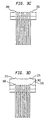
- Figs. 3a-e show a process of forming an array of trench capacitors.
- a substrate 301 is provided in which the trench capacitors are to be formed.
- the substrate for example, is a silicon wafer.
- Other semiconductor substrates such as gallium arsenide, germanium, silicon on insulator (SOI), or other semiconductor materials, are also useful.
- the substrate for example, may be lightly or heavily doped with dopants of a pre-determined conductivity to achieve the desired electrical characteristics.
- a pad stack layer 310 is formed on the surface of the substrate.
- the pad stack includes, for example, a pad oxide layer 312 formed on the surface of the substrate.
- the pad oxide is formed by, for example, thermal oxidation.
- the pad oxide is sufficiently thick to reduce stress and promote adhesion between a pad etch stop layer with the substrate.
- the pad etch stop layer should have sufficient selectivity to the material used to fill the trenches.
- the pad etch stop layer comprises silicon nitride (Si 3 N 4 ) due to its relatively low etch rate to the polysilicon used to fill the trenches.
- the etch selectivity between the poly and etch stop layers is about 60:1.
- the selectivity is about 300:1.
- the nitride layer is formed by, for example, low pressure chemical vapor deposition (LPCVD). Other techniques for depositing the nitride layer are also useful.
- the pad nitride layer is about 200nm.
- the hard etch mask comprises a material that is sufficiently dense or hard to withstand the ion bombardments of RIE during the formation of deep trenches.
- the thickness of the hard mask layer should be sufficient to prevent the deep trench etch from exposing the nitride layer. Further, the etch mask should have a higher wet etch rate than that of the pad etch stop layer. Typically, the selectivity is greater than about 80.
- the first hard mask layer comprises undoped silicate glass such as TEOS.
- a mask layer is deposited on the pad stack.
- the mask layer is patterned to create a block 320 that covers an array region of the substrate in which deep trenches are to be created.
- the block serves as an etch mask to protect the pad stack in the array region from being etched.
- the mask layer comprises a resist material.
- the resist is patterned by selectively exposing the resist with an exposure source and a mask containing the desired pattern. The resist is then developed to remove either the exposed or unexposed portions depending on whether a positive or negative resist is used, resulting in the formation of the block mask 320.
- the mask layer 316 in regions unprotected by the block mask is partially removed. Removal of the mask layer can be achieved by an RIE. Other etch techniques are also useful.
- the unprotected regions represent field regions of the substrate.
- the depth of the etch is substantially equal to about the amount of height differential of the mask layer between the array and field regions after the DT etch as a result of the different erosion rates between the two regions. Typically, the depth of the etch is about 8nm. Of course, the actual depth cf the field etch may vary depending on the erosion rate differential of the mask layer between the field and array regions.
- the block mask is removed after the partial field etch of the mask layer.
- the pad stack 310 is patterned using conventional lithographic techniques. Such techniques include depositing a photoresist layer over the pad stack and selectively exposing it with an exposure source and mask. Depending on whether a positive or negative resist is used, either the exposed or unexposed portions of the resist layer are removed during development, leaving regions of the pad stack unprotected. The unprotected regions correspond to areas where trenches are to be formed.
- An etch such as a reactive ion etch (RIE) is performed to create openings in the pad stack in regions unprotected by the resist.
- the openings expose the substrate below.
- a RIE then etches the substrate to create the DTs.
- the RIE erodes the pad mask in the array region. Since the pad mask in the field region has been partially etched to mask the excess erosion of the mask layer in the array region, the top surfaces of the pad mask in the field and array regions are substantially co-planar after the DT etch.
- ears 360 of the mask layer that are relatively small in height protrude above the pad mask at the array edge.
- the width of these features depends on the actual shape of the field etch blocking mask.
- diffusion regions surrounding the lower portion of the trenches are formed, serving as buried plates. Formation of the buried plates is achieved by various known techniques such as providing a source from which dopants diffuse into the substrate. Node dielectric of the capacitors is then formed in the trenches.
- poly 370 is deposited to fill the trenches. To ensure completely filling the trenches, the poly overfills the trench, resulting in excess poly that covers the surface of the substrate. Since poly is conformal, the ears 375 are present on the surface of the poly layer as a result of ears 360 on the mask layer below. Since ears 360 are relatively small in height, ears 375 are also relatively small in height.
- the excess poly is polished by, for example, CMP.
- the CMP is selective to the mask layer, removing the poly and using the mask layer as a stop layer. Since the field-array topography is avoided due to the partial field etch, the CMP is able to remove the poly without leaving any residuals at the edge of the array.
- the mask layer is removed by, for example, a wet etch.
- the wet etch is selective to the nitride and poly.
- the wet etch results in poly ears 380 protruding above the surface of the nitride-layer. Since the previous CMP process avoids leaving poly residuals, the height of the poly layers are substantially equal throughout the array regions. This advantageously eliminates the need of a touch up CMP process.
- the poly ears 380 are removed by an anisotropic etch used to recess the poly in the trenches to form the collar. As such, erosion of the pad nitride, as shown in Fig. 1d is avoided, resulting in improved yields.
- an etch such as an RIE is performed to recess the poly in the trenches to form a dielectric collar therein.
- the remaining portion of the DRAM is fabricated using conventional techniques, such as those described in Nesbit et al., A 0.6 ' ⁇ m 2 256Mb Trench DRAM Cell With Self-Aligned Buried Strap (BEST) , IEDM 93-627.
Landscapes
- Engineering & Computer Science (AREA)
- Manufacturing & Machinery (AREA)
- Semiconductor Memories (AREA)
- Drying Of Semiconductors (AREA)
- Mechanical Treatment Of Semiconductor (AREA)
- Formation Of Insulating Films (AREA)
Claims (1)
- Procédé de réduction d'une érosion excessive dans la fabrication d'un circuit intégré, comprenant les étapes consistant à :utiliser un substrat sur lequel est formée une pile de masquage (310), la pile de masquage comprenant une couche de masque dure (316) sur une couche d'arrêt de gravure à l'eau forte (314), le substrat comprenant une première zone dans laquelle doit être formé un réseau de condensateurs en tranchée, et une seconde zone à l'extérieur de la première zone ;former un masque de blocage (320) pour protéger la première zone ;graver partiellement à l'eau forte la couche de masque dure (316) dans la seconde zone, tandis que la première zone est protégée par le masque de blocage pendant la gravure partielle ;retirer le masque de blocage (320) ;tracer un motif sur la pile de masquage (310) pour exposer des parties du substrat dans la première zone où doit être formé le réseau de tranchées profondes ;graver le substrat à l'eau forte pour former les tranchées profondes, de façon que la gravure érode une certaine épaisseur de la couche de masque dure (316) dans la première zone, à un taux supérieur à celui de l'épaisseur de la couche de masque dure (316) dans la seconde zone, la gravure aboutissant à ce que la couche de masque dure présente une surface essentiellement plane dans les première et seconde zones du fait de la gravure partielle de la couche de masque dure dans la seconde zone ;remplir les tranchées profondes d'un matériau (370) pour former un noeud de stockage des condensateurs en tranchée ; eteffectuer un polissage pour retirer le matériau en excès de manière à exposer la couche de masque dure (316).
Applications Claiming Priority (2)
| Application Number | Priority Date | Filing Date | Title |
|---|---|---|---|
| US08/940,233 US5907771A (en) | 1997-09-30 | 1997-09-30 | Reduction of pad erosion |
| US940233 | 1997-09-30 |
Publications (3)
| Publication Number | Publication Date |
|---|---|
| EP0905749A2 EP0905749A2 (fr) | 1999-03-31 |
| EP0905749A3 EP0905749A3 (fr) | 2000-01-12 |
| EP0905749B1 true EP0905749B1 (fr) | 2002-10-30 |
Family
ID=25474462
Family Applications (1)
| Application Number | Title | Priority Date | Filing Date |
|---|---|---|---|
| EP98115707A Expired - Lifetime EP0905749B1 (fr) | 1997-09-30 | 1998-08-20 | Réduction d'érosion de couches de masquage |
Country Status (7)
| Country | Link |
|---|---|
| US (1) | US5907771A (fr) |
| EP (1) | EP0905749B1 (fr) |
| JP (1) | JPH11177064A (fr) |
| KR (1) | KR100504262B1 (fr) |
| CN (1) | CN1134838C (fr) |
| DE (1) | DE69809012T2 (fr) |
| TW (1) | TW426949B (fr) |
Families Citing this family (11)
| Publication number | Priority date | Publication date | Assignee | Title |
|---|---|---|---|---|
| US6190955B1 (en) * | 1998-01-27 | 2001-02-20 | International Business Machines Corporation | Fabrication of trench capacitors using disposable hard mask |
| US6440858B1 (en) * | 1998-08-24 | 2002-08-27 | International Business Machines Corporation | Multi-layer hard mask for deep trench silicon etch |
| US6734108B1 (en) * | 1999-09-27 | 2004-05-11 | Cypress Semiconductor Corporation | Semiconductor structure and method of making contacts in a semiconductor structure |
| US20060261436A1 (en) * | 2005-05-19 | 2006-11-23 | Freescale Semiconductor, Inc. | Electronic device including a trench field isolation region and a process for forming the same |
| US20070249127A1 (en) * | 2006-04-24 | 2007-10-25 | Freescale Semiconductor, Inc. | Electronic device including a semiconductor layer and a sidewall spacer and a process of forming the same |
| US7670895B2 (en) | 2006-04-24 | 2010-03-02 | Freescale Semiconductor, Inc | Process of forming an electronic device including a semiconductor layer and another layer adjacent to an opening within the semiconductor layer |
| US7491622B2 (en) * | 2006-04-24 | 2009-02-17 | Freescale Semiconductor, Inc. | Process of forming an electronic device including a layer formed using an inductively coupled plasma |
| US7528078B2 (en) | 2006-05-12 | 2009-05-05 | Freescale Semiconductor, Inc. | Process of forming electronic device including a densified nitride layer adjacent to an opening within a semiconductor layer |
| KR101075490B1 (ko) * | 2009-01-30 | 2011-10-21 | 주식회사 하이닉스반도체 | 매립게이트를 구비한 반도체장치 및 그 제조 방법 |
| KR20140145419A (ko) * | 2013-06-13 | 2014-12-23 | 삼성전자주식회사 | 반도체 소자 제조 방법 |
| CN111900168A (zh) * | 2016-01-25 | 2020-11-06 | 中国科学院微电子研究所 | 存储单元、存储器件及电子设备 |
Family Cites Families (7)
| Publication number | Priority date | Publication date | Assignee | Title |
|---|---|---|---|---|
| US4939104A (en) * | 1984-10-31 | 1990-07-03 | Texas Instruments, Incorporated | Method for forming a buried lateral contact |
| US5118384A (en) * | 1990-04-03 | 1992-06-02 | International Business Machines Corporation | Reactive ion etching buffer mask |
| JPH05110017A (ja) * | 1991-10-18 | 1993-04-30 | Hitachi Ltd | 半導体装置とその製造方法 |
| JP3439493B2 (ja) * | 1992-12-01 | 2003-08-25 | 沖電気工業株式会社 | 半導体記憶装置の製造方法 |
| DE19600423C2 (de) * | 1996-01-08 | 2001-07-05 | Siemens Ag | Elektrisch programmierbare Speicherzellenanordnung und Verfahren zu deren Herstellung |
| US5686345A (en) * | 1996-01-30 | 1997-11-11 | International Business Machines Corporation | Trench mask for forming deep trenches in a semiconductor substrate, and method of using same |
| US5776808A (en) * | 1996-12-26 | 1998-07-07 | Siemens Aktiengesellschaft | Pad stack with a poly SI etch stop for TEOS mask removal with RIE |
-
1997
- 1997-09-30 US US08/940,233 patent/US5907771A/en not_active Expired - Lifetime
-
1998
- 1998-08-11 TW TW087113184A patent/TW426949B/zh not_active IP Right Cessation
- 1998-08-13 CN CNB981184197A patent/CN1134838C/zh not_active Expired - Fee Related
- 1998-08-20 EP EP98115707A patent/EP0905749B1/fr not_active Expired - Lifetime
- 1998-08-20 DE DE69809012T patent/DE69809012T2/de not_active Expired - Lifetime
- 1998-09-29 KR KR10-1998-0040454A patent/KR100504262B1/ko not_active Expired - Fee Related
- 1998-09-30 JP JP10278460A patent/JPH11177064A/ja active Pending
Also Published As
| Publication number | Publication date |
|---|---|
| DE69809012T2 (de) | 2004-02-26 |
| KR100504262B1 (ko) | 2005-09-26 |
| TW426949B (en) | 2001-03-21 |
| KR19990030229A (ko) | 1999-04-26 |
| EP0905749A3 (fr) | 2000-01-12 |
| EP0905749A2 (fr) | 1999-03-31 |
| DE69809012D1 (de) | 2002-12-05 |
| JPH11177064A (ja) | 1999-07-02 |
| CN1213171A (zh) | 1999-04-07 |
| CN1134838C (zh) | 2004-01-14 |
| US5907771A (en) | 1999-05-25 |
Similar Documents
| Publication | Publication Date | Title |
|---|---|---|
| US6727539B2 (en) | Embedded vertical DRAM arrays with silicided bitline and polysilicon interconnect | |
| EP0905755B1 (fr) | Procédé d'amélioration de la résistance à l'effet de cuvette | |
| US6020091A (en) | Hard etch mask | |
| US5867420A (en) | Reducing oxidation stress in the fabrication of devices | |
| EP0948043B1 (fr) | Méthode avec une controlabilité améliorée d'une couche enterrée | |
| US6124206A (en) | Reduced pad erosion | |
| US6033997A (en) | Reduction of black silicon in semiconductor fabrication | |
| EP0905749B1 (fr) | Réduction d'érosion de couches de masquage | |
| US6812091B1 (en) | Trench capacitor memory cell | |
| KR100309619B1 (ko) | 스페이서를이용한집적회로형성방법 | |
| EP0942461A2 (fr) | Réduction du silicium noir dans la fabrication des semiconducteurs | |
| HK1017492A (en) | Reduction of pad erosion | |
| HK1018350A (en) | Reduced etch stop layer erosion | |
| HK1018352A (en) | Reduction of black silicon in semiconductor fabrication | |
| HK1021252A (en) | Reduction of black silicon in semiconductor fabrication | |
| HK1017491A (en) | Process to improve dishing resistance | |
| HK1019961A (en) | Method with improved controllability of a buried layer | |
| HK1017502A (en) | Hard etch mask | |
| HK1017139A (en) | Shallow trench isolation for dram trench capacitor |
Legal Events
| Date | Code | Title | Description |
|---|---|---|---|
| PUAI | Public reference made under article 153(3) epc to a published international application that has entered the european phase |
Free format text: ORIGINAL CODE: 0009012 |
|
| AK | Designated contracting states |
Kind code of ref document: A2 Designated state(s): DE FR GB IE IT NL |
|
| AX | Request for extension of the european patent |
Free format text: AL;LT;LV;MK;RO;SI |
|
| PUAL | Search report despatched |
Free format text: ORIGINAL CODE: 0009013 |
|
| AK | Designated contracting states |
Kind code of ref document: A3 Designated state(s): AT BE CH CY DE DK ES FI FR GB GR IE IT LI LU MC NL PT SE |
|
| AX | Request for extension of the european patent |
Free format text: AL;LT;LV;MK;RO;SI |
|
| RIC1 | Information provided on ipc code assigned before grant |
Free format text: 7H 01L 21/8242 A, 7H 01L 21/311 B |
|
| 17P | Request for examination filed |
Effective date: 20000226 |
|
| AKX | Designation fees paid |
Free format text: DE FR GB IE IT NL |
|
| 17Q | First examination report despatched |
Effective date: 20001020 |
|
| GRAG | Despatch of communication of intention to grant |
Free format text: ORIGINAL CODE: EPIDOS AGRA |
|
| GRAG | Despatch of communication of intention to grant |
Free format text: ORIGINAL CODE: EPIDOS AGRA |
|
| GRAH | Despatch of communication of intention to grant a patent |
Free format text: ORIGINAL CODE: EPIDOS IGRA |
|
| GRAH | Despatch of communication of intention to grant a patent |
Free format text: ORIGINAL CODE: EPIDOS IGRA |
|
| GRAA | (expected) grant |
Free format text: ORIGINAL CODE: 0009210 |
|
| AK | Designated contracting states |
Kind code of ref document: B1 Designated state(s): DE FR GB IE IT NL |
|
| REG | Reference to a national code |
Ref country code: GB Ref legal event code: FG4D |
|
| REG | Reference to a national code |
Ref country code: IE Ref legal event code: FG4D |
|
| REF | Corresponds to: |
Ref document number: 69809012 Country of ref document: DE Date of ref document: 20021205 |
|
| RAP2 | Party data changed (patent owner data changed or rights of a patent transferred) |
Owner name: INFINEON TECHNOLOGIES AG |
|
| NLT2 | Nl: modifications (of names), taken from the european patent patent bulletin |
Owner name: INFINEON TECHNOLOGIES AG |
|
| ET | Fr: translation filed | ||
| PLBE | No opposition filed within time limit |
Free format text: ORIGINAL CODE: 0009261 |
|
| STAA | Information on the status of an ep patent application or granted ep patent |
Free format text: STATUS: NO OPPOSITION FILED WITHIN TIME LIMIT |
|
| 26N | No opposition filed |
Effective date: 20030731 |
|
| PGFP | Annual fee paid to national office [announced via postgrant information from national office to epo] |
Ref country code: GB Payment date: 20050808 Year of fee payment: 8 |
|
| REG | Reference to a national code |
Ref country code: HK Ref legal event code: WD Ref document number: 1017492 Country of ref document: HK |
|
| GBPC | Gb: european patent ceased through non-payment of renewal fee |
Effective date: 20060820 |
|
| PGFP | Annual fee paid to national office [announced via postgrant information from national office to epo] |
Ref country code: IE Payment date: 20070824 Year of fee payment: 10 |
|
| PG25 | Lapsed in a contracting state [announced via postgrant information from national office to epo] |
Ref country code: GB Free format text: LAPSE BECAUSE OF NON-PAYMENT OF DUE FEES Effective date: 20060820 |
|
| PGFP | Annual fee paid to national office [announced via postgrant information from national office to epo] |
Ref country code: IT Payment date: 20070824 Year of fee payment: 10 |
|
| PGFP | Annual fee paid to national office [announced via postgrant information from national office to epo] |
Ref country code: FR Payment date: 20070812 Year of fee payment: 10 |
|
| PGFP | Annual fee paid to national office [announced via postgrant information from national office to epo] |
Ref country code: NL Payment date: 20080813 Year of fee payment: 11 |
|
| REG | Reference to a national code |
Ref country code: IE Ref legal event code: MM4A |
|
| REG | Reference to a national code |
Ref country code: FR Ref legal event code: ST Effective date: 20090430 |
|
| PG25 | Lapsed in a contracting state [announced via postgrant information from national office to epo] |
Ref country code: IE Free format text: LAPSE BECAUSE OF NON-PAYMENT OF DUE FEES Effective date: 20080820 |
|
| PG25 | Lapsed in a contracting state [announced via postgrant information from national office to epo] |
Ref country code: IT Free format text: LAPSE BECAUSE OF NON-PAYMENT OF DUE FEES Effective date: 20080820 Ref country code: FR Free format text: LAPSE BECAUSE OF NON-PAYMENT OF DUE FEES Effective date: 20080901 |
|
| REG | Reference to a national code |
Ref country code: NL Ref legal event code: V1 Effective date: 20100301 |
|
| PG25 | Lapsed in a contracting state [announced via postgrant information from national office to epo] |
Ref country code: NL Free format text: LAPSE BECAUSE OF NON-PAYMENT OF DUE FEES Effective date: 20100301 |
|
| REG | Reference to a national code |
Ref country code: DE Ref legal event code: R081 Ref document number: 69809012 Country of ref document: DE Owner name: POLARIS INNOVATIONS LTD., IE Free format text: FORMER OWNER: QIMONDA AG, 81739 MUENCHEN, DE Ref country code: DE Ref legal event code: R081 Ref document number: 69809012 Country of ref document: DE Owner name: INFINEON TECHNOLOGIES AG, DE Free format text: FORMER OWNER: QIMONDA AG, 81739 MUENCHEN, DE |
|
| REG | Reference to a national code |
Ref country code: DE Ref legal event code: R081 Ref document number: 69809012 Country of ref document: DE Owner name: POLARIS INNOVATIONS LTD., IE Free format text: FORMER OWNER: INFINEON TECHNOLOGIES AG, 85579 NEUBIBERG, DE |
|
| PGFP | Annual fee paid to national office [announced via postgrant information from national office to epo] |
Ref country code: DE Payment date: 20150929 Year of fee payment: 18 |
|
| REG | Reference to a national code |
Ref country code: DE Ref legal event code: R119 Ref document number: 69809012 Country of ref document: DE |
|
| PG25 | Lapsed in a contracting state [announced via postgrant information from national office to epo] |
Ref country code: DE Free format text: LAPSE BECAUSE OF NON-PAYMENT OF DUE FEES Effective date: 20170301 |