EP0905828A2 - Dispositif d'identification des appareils électroniques - Google Patents
Dispositif d'identification des appareils électroniques Download PDFInfo
- Publication number
- EP0905828A2 EP0905828A2 EP98117385A EP98117385A EP0905828A2 EP 0905828 A2 EP0905828 A2 EP 0905828A2 EP 98117385 A EP98117385 A EP 98117385A EP 98117385 A EP98117385 A EP 98117385A EP 0905828 A2 EP0905828 A2 EP 0905828A2
- Authority
- EP
- European Patent Office
- Prior art keywords
- conductor tracks
- area
- coding plug
- cutouts
- coding
- Prior art date
- Legal status (The legal status is an assumption and is not a legal conclusion. Google has not performed a legal analysis and makes no representation as to the accuracy of the status listed.)
- Withdrawn
Links
Images
Classifications
-
- H—ELECTRICITY
- H05—ELECTRIC TECHNIQUES NOT OTHERWISE PROVIDED FOR
- H05K—PRINTED CIRCUITS; CASINGS OR CONSTRUCTIONAL DETAILS OF ELECTRIC APPARATUS; MANUFACTURE OF ASSEMBLAGES OF ELECTRICAL COMPONENTS
- H05K7/00—Constructional details common to different types of electric apparatus
- H05K7/14—Mounting supporting structure in casing or on frame or rack
- H05K7/1438—Back panels or connecting means therefor; Terminals; Coding means to avoid wrong insertion
- H05K7/1452—Mounting of connectors; Switching; Reinforcing of back panels
- H05K7/1455—Coding for prevention of wrong insertion
-
- G—PHYSICS
- G06—COMPUTING OR CALCULATING; COUNTING
- G06K—GRAPHICAL DATA READING; PRESENTATION OF DATA; RECORD CARRIERS; HANDLING RECORD CARRIERS
- G06K19/00—Record carriers for use with machines and with at least a part designed to carry digital markings
- G06K19/04—Record carriers for use with machines and with at least a part designed to carry digital markings characterised by the shape
-
- H—ELECTRICITY
- H05—ELECTRIC TECHNIQUES NOT OTHERWISE PROVIDED FOR
- H05K—PRINTED CIRCUITS; CASINGS OR CONSTRUCTIONAL DETAILS OF ELECTRIC APPARATUS; MANUFACTURE OF ASSEMBLAGES OF ELECTRICAL COMPONENTS
- H05K1/00—Printed circuits
- H05K1/02—Details
- H05K1/0286—Programmable, customizable or modifiable circuits
- H05K1/0293—Individual printed conductors which are adapted for modification, e.g. fusable or breakable conductors, printed switches
-
- H—ELECTRICITY
- H05—ELECTRIC TECHNIQUES NOT OTHERWISE PROVIDED FOR
- H05K—PRINTED CIRCUITS; CASINGS OR CONSTRUCTIONAL DETAILS OF ELECTRIC APPARATUS; MANUFACTURE OF ASSEMBLAGES OF ELECTRICAL COMPONENTS
- H05K1/00—Printed circuits
- H05K1/02—Details
- H05K1/0266—Marks, test patterns or identification means
-
- H—ELECTRICITY
- H05—ELECTRIC TECHNIQUES NOT OTHERWISE PROVIDED FOR
- H05K—PRINTED CIRCUITS; CASINGS OR CONSTRUCTIONAL DETAILS OF ELECTRIC APPARATUS; MANUFACTURE OF ASSEMBLAGES OF ELECTRICAL COMPONENTS
- H05K1/00—Printed circuits
- H05K1/02—Details
- H05K1/0286—Programmable, customizable or modifiable circuits
- H05K1/029—Programmable, customizable or modifiable circuits having a programmable lay-out, i.e. adapted for choosing between a few possibilities
-
- H—ELECTRICITY
- H05—ELECTRIC TECHNIQUES NOT OTHERWISE PROVIDED FOR
- H05K—PRINTED CIRCUITS; CASINGS OR CONSTRUCTIONAL DETAILS OF ELECTRIC APPARATUS; MANUFACTURE OF ASSEMBLAGES OF ELECTRICAL COMPONENTS
- H05K1/00—Printed circuits
- H05K1/02—Details
- H05K1/03—Use of materials for the substrate
- H05K1/0393—Flexible materials
-
- H—ELECTRICITY
- H05—ELECTRIC TECHNIQUES NOT OTHERWISE PROVIDED FOR
- H05K—PRINTED CIRCUITS; CASINGS OR CONSTRUCTIONAL DETAILS OF ELECTRIC APPARATUS; MANUFACTURE OF ASSEMBLAGES OF ELECTRICAL COMPONENTS
- H05K1/00—Printed circuits
- H05K1/02—Details
- H05K1/11—Printed elements for providing electric connections to or between printed circuits
- H05K1/118—Printed elements for providing electric connections to or between printed circuits specially for flexible printed circuits, e.g. using folded portions
-
- H—ELECTRICITY
- H05—ELECTRIC TECHNIQUES NOT OTHERWISE PROVIDED FOR
- H05K—PRINTED CIRCUITS; CASINGS OR CONSTRUCTIONAL DETAILS OF ELECTRIC APPARATUS; MANUFACTURE OF ASSEMBLAGES OF ELECTRICAL COMPONENTS
- H05K2201/00—Indexing scheme relating to printed circuits covered by H05K1/00
- H05K2201/09—Shape and layout
- H05K2201/09009—Substrate related
- H05K2201/09063—Holes or slots in insulating substrate not used for electrical connections
-
- H—ELECTRICITY
- H05—ELECTRIC TECHNIQUES NOT OTHERWISE PROVIDED FOR
- H05K—PRINTED CIRCUITS; CASINGS OR CONSTRUCTIONAL DETAILS OF ELECTRIC APPARATUS; MANUFACTURE OF ASSEMBLAGES OF ELECTRICAL COMPONENTS
- H05K2201/00—Indexing scheme relating to printed circuits covered by H05K1/00
- H05K2201/09—Shape and layout
- H05K2201/09818—Shape or layout details not covered by a single group of H05K2201/09009 - H05K2201/09809
- H05K2201/0999—Circuit printed on or in housing, e.g. housing as PCB; Circuit printed on the case of a component; PCB affixed to housing
-
- H—ELECTRICITY
- H05—ELECTRIC TECHNIQUES NOT OTHERWISE PROVIDED FOR
- H05K—PRINTED CIRCUITS; CASINGS OR CONSTRUCTIONAL DETAILS OF ELECTRIC APPARATUS; MANUFACTURE OF ASSEMBLAGES OF ELECTRICAL COMPONENTS
- H05K2203/00—Indexing scheme relating to apparatus or processes for manufacturing printed circuits covered by H05K3/00
- H05K2203/01—Tools for processing; Objects used during processing
- H05K2203/0195—Tool for a process not provided for in H05K3/00, e.g. tool for handling objects using suction, for deforming objects, for applying local pressure
-
- H—ELECTRICITY
- H05—ELECTRIC TECHNIQUES NOT OTHERWISE PROVIDED FOR
- H05K—PRINTED CIRCUITS; CASINGS OR CONSTRUCTIONAL DETAILS OF ELECTRIC APPARATUS; MANUFACTURE OF ASSEMBLAGES OF ELECTRICAL COMPONENTS
- H05K2203/00—Indexing scheme relating to apparatus or processes for manufacturing printed circuits covered by H05K3/00
- H05K2203/17—Post-manufacturing processes
- H05K2203/175—Configurations of connections suitable for easy deletion, e.g. modifiable circuits or temporary conductors for electroplating; Processes for deleting connections
Definitions
- the invention relates to a device according to the features the preamble of claim 1.
- the present invention is based on the object for the data acquisition and transmission of the respective Information specifying the housing type if possible easy to implement device.
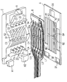
- This device consists of a total of three components, and from a coding area provided in a housing wall A, a strip line arrangement B and a coding plug C.
- the essential component that is unique Identification of the housing is possible in the housing wall A provided coding area by a combination of binary digits in the form of cutouts of a first and second type is formed. In the example shown, it is slot-like recesses running parallel to one another A1 ... A4, with the cutouts A2 and A4 by one each Crossbar Q2 and Q4 in two, preferably the same size Sections are divided.
- a coding plug C can be attached, the including several, the number of cutouts A1 to A4 has corresponding ridges S1 ... S4 arranged in the manner of a comb.
- this coding plug is now the end section of a strip line B put on the several, each the webs S1 ... S4 has assigned conductor tracks L1 ... L4.
- the stripline B consists of a thin, flexible, insulating carrier material, for example a film made of polyester, Polycarbonate or polyamide, on which several conductor tracks, for example by printing with silver conductive paste are applied.
- the stripline are the conductor tracks L1 ... L4 separated from each other by separating slots.
- these conductor tracks in the area of the crossbars of the coding area one predetermined breaking point SB1 ... SB4, their function will be explained later.
- the mechanical fixing of the coding plug C takes place on the one hand via gripping hooks H1, H2, those in openings D1, D2 in the housing wall A articulated be held and on the other hand by one opposite provided locking hook R, which in a corresponding Opening D3 is immersed in the housing wall A.
- the individual conductor tracks L1 ... L4 of the strip line B are connected at one end to an evaluation logic, each after whether the line is interrupted by shear at the crossbar Q2, Q4 is or not, query a corresponding binary signal can.
- the conductor tracks L1 ... L4 are on a common return line RL connected, too is returned to the evaluation logic and there to a reference potential connected isit.
- sensor functions for other physical quantities can be done by additional electronic components applied in the sensor area, e.g. B. temperature sensor T, and by additional signal lines for evaluation logic with the function of housing identification be combined.
Landscapes
- Engineering & Computer Science (AREA)
- Microelectronics & Electronic Packaging (AREA)
- Physics & Mathematics (AREA)
- General Physics & Mathematics (AREA)
- Theoretical Computer Science (AREA)
- Details Of Connecting Devices For Male And Female Coupling (AREA)
- Lock And Its Accessories (AREA)
Applications Claiming Priority (2)
| Application Number | Priority Date | Filing Date | Title |
|---|---|---|---|
| DE19743280 | 1997-09-30 | ||
| DE1997143280 DE19743280C1 (de) | 1997-09-30 | 1997-09-30 | Vorrichtung zur Identifizierung von elektronischen Geräten |
Publications (2)
| Publication Number | Publication Date |
|---|---|
| EP0905828A2 true EP0905828A2 (fr) | 1999-03-31 |
| EP0905828A3 EP0905828A3 (fr) | 1999-11-03 |
Family
ID=7844209
Family Applications (1)
| Application Number | Title | Priority Date | Filing Date |
|---|---|---|---|
| EP98117385A Withdrawn EP0905828A3 (fr) | 1997-09-30 | 1998-09-15 | Dispositif d'identification des appareils électroniques |
Country Status (2)
| Country | Link |
|---|---|
| EP (1) | EP0905828A3 (fr) |
| DE (1) | DE19743280C1 (fr) |
Families Citing this family (5)
| Publication number | Priority date | Publication date | Assignee | Title |
|---|---|---|---|---|
| DE19927795C2 (de) * | 1999-06-18 | 2002-01-10 | Phoenix Contact Gmbh & Co | Leiterplatte für eine Schaltunsanordnung |
| DE19931003C2 (de) * | 1999-07-05 | 2001-04-26 | Siemens Ag | Sichtbare Identifikation von elektronischen Systemen |
| DE10006112A1 (de) * | 2000-02-11 | 2001-08-16 | Draexlmaier Lisa Gmbh | Verbinder für Folienleiter |
| DE10062912A1 (de) * | 2000-12-16 | 2002-07-11 | Buhler Motor Gmbh | Adressierung eines busgesteuerten Stellantriebs |
| DE102021214773A1 (de) | 2021-12-21 | 2023-06-22 | Robert Bosch Gesellschaft mit beschränkter Haftung | Elektronikeinheit mit einer Leiterplatte zu einer Anordnung in einer elektrischen Vorrichtung sowie elektrische Vorrichtung mit einem Gehäuseteil zur Aufnahme der Elektronikeinheit |
Family Cites Families (5)
| Publication number | Priority date | Publication date | Assignee | Title |
|---|---|---|---|---|
| US4471158A (en) * | 1981-12-11 | 1984-09-11 | Advanced Circuit Technology, Inc. | Programmable header |
| US4704505A (en) * | 1986-08-06 | 1987-11-03 | Illinois Tool Works Inc. | Electrical apparatus configured for predetermined encoding |
| FR2636175B1 (fr) * | 1988-09-02 | 1990-11-23 | Apr Composants | Dispositif de codage notamment pour carte a circuits integres |
| US5330370A (en) * | 1991-11-04 | 1994-07-19 | Spectra-Physics Scanning Systems, Inc. | Multiple-interface selection system for computer peripherals |
| US5314346A (en) * | 1992-12-18 | 1994-05-24 | International Business Machines Corporation | Flexible circuit applique patch customization for generic programmable cable assemblies |
-
1997
- 1997-09-30 DE DE1997143280 patent/DE19743280C1/de not_active Expired - Fee Related
-
1998
- 1998-09-15 EP EP98117385A patent/EP0905828A3/fr not_active Withdrawn
Also Published As
| Publication number | Publication date |
|---|---|
| DE19743280C1 (de) | 1998-10-08 |
| EP0905828A3 (fr) | 1999-11-03 |
Similar Documents
| Publication | Publication Date | Title |
|---|---|---|
| EP0289519B1 (fr) | Procede et dispositif pour determiner l'identite et la position d'objets | |
| DE2414566C2 (de) | Elektrisches Automatiksystem | |
| EP0285799A2 (fr) | Dispositif de test électrique du fonctionnement de rangées de fils électriques, en particulier pour cartes de circuit | |
| DE2821987A1 (de) | Markierungsleser | |
| EP0078339A1 (fr) | Dispositif de test pour pistes de circuit imprimé ayant au moins une tête comportant une multitude de contacts flexibles | |
| EP0177019A2 (fr) | Dispositif de transmission de données comprenant un réseau de données à structure en arbre | |
| DE29901194U1 (de) | Busleiterabschnitt für ein elektrisches Gerät | |
| DE2717372B2 (de) | Baugruppe aus einem Digitalschalter und elektronischen Bauelementen | |
| EP0905828A2 (fr) | Dispositif d'identification des appareils électroniques | |
| DE102017127792A1 (de) | Vorrichtung und Verfahren zur Leitungslängenbestimmung | |
| DE2655841C3 (de) | Integrierter Widerstandsbaustein zum Einlöten in eine Flachbaugruppe | |
| DE69008217T2 (de) | System zum Prüfen von Kabelstücken. | |
| EP0098554B1 (fr) | Procédé et dispositif pour la demande automatique des valeurs de mesure de signalisation et de l'identificateur de signalisation dans une installation d'avertisseur d'alarme | |
| EP0679054A2 (fr) | Dispositif pour codage de circuits imprimés | |
| EP1031042B1 (fr) | Dispositif pour verifier des cartes de circuits | |
| DE4328932A1 (de) | Verfahren und Einrichtung für die Fernabfrage von Meßstellen | |
| DE2017151A1 (de) | Testadapter für Schaltungskarten | |
| EP1166395A1 (fr) | Appareil pourvu d'un dispositif de mise en contact destine a un cable plat a forme codee | |
| DE3540434A1 (de) | Schaltungsanordnung zum abfragen des zustands wenigstens einer tasteinrichtung und liefern einer anzeige durch eine anzeigeeinrichtung | |
| DE2337987C3 (de) | Zum Einbau in eine Steuervorrichtung vorgesehene Rangierleiste | |
| DE68923554T2 (de) | Antistatischer abfrageverbinder für elektrische komponenten. | |
| DE4009296C2 (fr) | ||
| EP1083434A2 (fr) | Appareil pour tester des plaquettes de circuits imprimés | |
| DE3642587A1 (de) | Vorrichtung zum voraltern von ic-baueinheiten | |
| DE3634181C2 (fr) |
Legal Events
| Date | Code | Title | Description |
|---|---|---|---|
| PUAI | Public reference made under article 153(3) epc to a published international application that has entered the european phase |
Free format text: ORIGINAL CODE: 0009012 |
|
| AK | Designated contracting states |
Kind code of ref document: A2 Designated state(s): DE FI FR GB IE IT NL SE |
|
| AX | Request for extension of the european patent |
Free format text: AL;LT;LV;MK;RO;SI |
|
| PUAL | Search report despatched |
Free format text: ORIGINAL CODE: 0009013 |
|
| AK | Designated contracting states |
Kind code of ref document: A3 Designated state(s): AT BE CH CY DE DK ES FI FR GB GR IE IT LI LU MC NL PT SE |
|
| AX | Request for extension of the european patent |
Free format text: AL;LT;LV;MK;RO;SI |
|
| RIC1 | Information provided on ipc code assigned before grant |
Free format text: 6H 01R 29/00 A, 6H 05K 1/00 B |
|
| 17P | Request for examination filed |
Effective date: 20000503 |
|
| AKX | Designation fees paid |
Free format text: DE FI FR GB IE IT NL SE |
|
| RAP1 | Party data changed (applicant data changed or rights of an application transferred) |
Owner name: FUJITSU SIEMENS COMPUTERS GMBH |
|
| RAP1 | Party data changed (applicant data changed or rights of an application transferred) |
Owner name: FUJITSU SIEMENS COMPUTERS GMBH |
|
| STAA | Information on the status of an ep patent application or granted ep patent |
Free format text: STATUS: THE APPLICATION HAS BEEN WITHDRAWN |
|
| 18W | Application withdrawn |
Effective date: 20050224 |