EP0905883A2 - Circuit de compensation de température pour amplificateurs à transistors à effet de champs - Google Patents
Circuit de compensation de température pour amplificateurs à transistors à effet de champs Download PDFInfo
- Publication number
- EP0905883A2 EP0905883A2 EP98116208A EP98116208A EP0905883A2 EP 0905883 A2 EP0905883 A2 EP 0905883A2 EP 98116208 A EP98116208 A EP 98116208A EP 98116208 A EP98116208 A EP 98116208A EP 0905883 A2 EP0905883 A2 EP 0905883A2
- Authority
- EP
- European Patent Office
- Prior art keywords
- effect transistor
- field effect
- drain current
- temperature compensation
- compensation circuit
- Prior art date
- Legal status (The legal status is an assumption and is not a legal conclusion. Google has not performed a legal analysis and makes no representation as to the accuracy of the status listed.)
- Withdrawn
Links
Images

Classifications
-
- H—ELECTRICITY
- H03—ELECTRONIC CIRCUITRY
- H03F—AMPLIFIERS
- H03F1/00—Details of amplifiers with only discharge tubes, only semiconductor devices or only unspecified devices as amplifying elements
- H03F1/30—Modifications of amplifiers to reduce influence of variations of temperature or supply voltage or other physical parameters
- H03F1/301—Modifications of amplifiers to reduce influence of variations of temperature or supply voltage or other physical parameters in MOSFET amplifiers
Definitions
- the present invention relates to a temperature compensation circuit for voltage controlled amplifiers and in particular to a temperature compensation circuit for field effect transistor amplifier circuits.
- AGC automatic Gain control
- the gain control in bipolar transistor or MOSFET amplifier stages can be shifted the operating point of the transistor or FETs with multiple control inputs (e.g. dual-gate MOSFETs) be used.
- JP07-162241A is a temperature compensation circuit known for a field effect transistor amplifier, the a resistor connected in series to the drain of the field effect transistor has to by measuring the above this Resistance falling voltage using an operational amplifier generate a signal dependent on the drain current, which is used as the input signal of a controller whose Output connected to the gate of the field effect transistor is to regulate the drain current to a constant value.
- JP06-29751A is a temperature compensation circuit known for a dual gate MOSFET.
- the present The invention is therefore based on the object of a temperature compensation circuit for a field effect transistor amplifier circuit to create in the entire operating temperature range to achieve full temperature compensation.
- This task is accomplished through a temperature compensation circuit for a field effect transistor amplifier circuit according to Claim 1 solved.
- the present invention provides a temperature compensation circuit for a field effect transistor amplifier circuit, with the following features: a current detection device for detecting the actual drain current of the field effect transistor; a control device with an input, which is connected to an output of the current detection device and an output that is connected to a control input of the Field effect transistor is connected to regulate the actual drain current of the field effect transistor to a target drain current, the target drain current being such a drain current corresponds in which the relationship between drain current and The slope of the field effect transistor is essentially independent of temperature is.
- the present invention is particularly advantageous in such cases Applications can be used in which the control voltage of a voltage controlled amplifier evaluated as a measured variable is used, for example, for damping measurement in one closed loop.
- the temperature compensation circuit according to the invention is particularly in such amplifier circuits can be used advantageously by means of MOS field-effect transistors (MOSFET) or dual-gate MOS field-effect transistors (Dual gate MOSFET) are realized.
- MOSFET MOS field-effect transistors
- Dual gate MOSFET dual-gate MOS field-effect transistors
- the present invention is based on the finding that that full temperature compensation, i.e. H. for example a complete temperature independence of the Measurement results in the above-mentioned damping measurement, and thus the gain behavior of a field effect transistor reached over the entire operating temperature range can be used when the drain current of the Field effect transistor set to a range of values and is governed by the relationship between the slope and the drain current of a field effect transistor essentially is completely independent of temperature.
- the current detection device by a Current mirror circuit can be implemented while the controller device for regulating the drain current using a proportional-integral controller (PI controller) can be designed which is preferably operated in the aperiodic limit case.
- PI controller proportional-integral controller
- the present invention is based on a preferred embodiment of the same, which relates to a Dual-gate MOSFET relates, explained in more detail.
- the temperature compensation circuit according to the invention can also be used for other field effect transistors is.
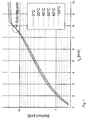
- FIG. 1 shows the relationship between the slope [mS] and the drain current I D [mA] of a MOSFET as a function of the temperature.
- the inventor surprisingly observed both in the simulation and experimentally that the relationship between the drain current I D and the slope g m is almost independent of temperature, with an area in which the temperature dependence is almost zero can be seen from FIG. 1 (intersection ). Since the slope characterizes the actual control effect of a MOSFET, it is now desirable to keep the drain current I D of a MOSFET in the range in which the relationship between drain current I D and slope g m has no temperature dependence.
- the principle of temperature stabilization or temperature compensation of a field effect transistor amplifier circuit is based on the measurement of the drain current I D as the actual value for a controller, e.g. B. a PI controller, which keeps the drain current I D constant by means of a suitable control variable (e.g. the gate voltage of the MOSFET).
- the setpoint for the controller is expediently chosen for an amplifier with a fixed gain so that the drain current I D is in the region of the intersection (see FIG. 1).
- the setpoint of the drain current I D is used as a manipulated variable.
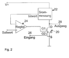
- 20 denotes a dual gate MOSFET of a field effect transistor amplifier circuit.
- the source terminal S of the MOSFET 20 is grounded, while a current detection device 22 is connected between the drain terminal D of the MOSFET 20 and a supply voltage V + .
- the output of the current detection device, on which a signal representing the detected current is present, is connected to an input of a controller 24.
- a second input of the controller 24 can be supplied with a setpoint.
- the output of the regulator 24 is connected to a first gate connection G1 of the dual-gate MOSFET 20.
- a second gate terminal G2 of the MOSFET 20 is connected to the input 26 of the amplifier circuit.
- the output 28 of the amplifier circuit is connected to the drain terminal D of the MOSFET 20.
- a bulk terminal B of MOSFET 20 is also connected to ground.
- the supply voltage V + applied to the current detection device 22 causes a drain current I D of the MOS field-effect transistor 20.
- a signal, actual value, is generated at the output of the current detection device 22 and represents the drain current I D at the drain terminal D of the MOSFET 20. In the exemplary embodiment shown, this signal is fed to the inverting input of a differential amplifier, which represents the controller 24. A signal is supplied to the non-inverting input of the differential amplifier, which corresponds to the target value of the drain current I D.
- the signal which arises at the output of the regulator 24 is then fed to a suitable control connection of the MOSFET 20, ie in the exemplary embodiment shown, the gate connection G1 of the MOSFET, as a result of which the drain current I D of the MOSFET 20 is always at a fixed value predetermined by the setpoint V GC Level is maintained.
- This level for the drain current I D suitably corresponds to the drain current I D at the intersection (see FIG. 1), at which the relationship between the slope and drain current of the MOS field-effect transistor are essentially completely temperature-independent over the entire operating temperature range of the amplifier arrangement.
- An input signal present at the input 26 of the amplifier arrangement is fed into the gate connection G2 of the MOS field-effect transistor 20 and then processed or amplified by the MOSFET amplifier arrangement and can be tapped off at the output 28 of the amplifier arrangement as an output signal.
- the Drain current through the control device shown in Fig. 2 stabilized, i.e. regulated to the setpoint. Because the drain current to a setpoint that is in a range lies in which the connection between drain current and Slope in the entire operating temperature range essentially is temperature-independent, affect temperature fluctuations the amplification behavior of the amplifier circuit Not.
- Fig. 3 is the temperature compensation circuit for a MOS field effect transistor amplifier circuit in more detail shown.
- the supply voltage V + which is provided by a current / voltage supply source (not shown), is connected via a first resistor R1 to the second gate terminal G2 of the dual-gate MOSFET 20.
- This gate connection G2 of the MOSFET 20 is connected to ground via a second resistor R2.
- the two resistors R1, R2 form a voltage divider with respect to the voltage V + in order to bring the MOSFET into a range which is favorable for the application.
- the input 26 of the amplifier circuit is connected to the second gate terminal G2 of the MOSFET 20 via a coupling capacitor C1.
- the current detection device is formed by a current mirror circuit which has two bipolar transistors T 1 , T 2 .
- Such current mirror circuits are known in the art. However, it is obvious that other current detection devices can be used in addition to the current mirror circuit shown.
- the emitter connections E1 and E2 of the two bipolar transistors T1, T2 are connected to the supply voltage V + .
- the base connection B1 of the first bipolar transistor T1 is connected to the base connection B2 of the second bipolar transistor T2, the collector connection K2 of the bipolar transistor T2 also being fed back to its base connection B2.
- the collector connection K2 of the bipolar transistor T2 is connected to the drain connection D of the MOSFET 20 via an inductance L1.
- the drain terminal D of the MOSFET 20 is also connected via a coupling capacitor C4 to the output 28 of the circuit arrangement.
- the source terminal S and the bulk terminal B of the MOSFET 20 are connected to one another and are grounded.
- the collector terminal K1 of the bipolar transistor T1 is connected via a third resistor R3 to the inverting input of an operational amplifier OP1. Furthermore, the collector terminal K1 is connected to ground via a parallel connection of a third capacitor C3 and a fourth resistor R4.
- the inverting input of an operational amplifier OP1 is connected via a second capacitor C2 to the output of the operational amplifier OP1, the output of the operational amplifier OP1 also being connected to the gate terminal G1 of the field effect transistor 20.
- a signal V GC is present at the non-inverting input of the operational amplifier OP1.
- the operational amplifier OP1, the second capacitor C2 and the third resistor R3 represent a proportional-integral controller (PI controller) in the connection described, which forms the controller 24 in this exemplary embodiment.
- PI controller proportional-integral controller
- a dual-gate MOSFET was chosen because it allows the high-frequency and the control circuit to be separated.
- the MOS field-effect transistor 20 is brought into a working range which is favorable for the application by means of the voltage divider of the voltage V + at the gate G1 of the transistor T3 formed from the resistors R1, R2.
- the current mirror circuit which consists of the transistors T1, T2, reflects the drain current I D in the control loop. Because of the short-circuit formation between collector K2 and base B2, transistor T2 always works in the active region.
- the base-emitter voltage is inevitably the same for both transistors T1, T2, so that with the same transistor systems and the same temperature, the collector currents of the transistors also match.
- This mirror current which is formed by the collector current of the transistor T1 generates a voltage drop across the resistor R4, which represents the actual value of the drain current I D.
- This voltage drop is applied to the PI controller, which is formed by the operational amplifier connected to the resistor R3 and the capacitor C2.
- the characteristic sizes of the controller are preferably set so that the controller operates in the aperiodic limit case.
- the capacitor C3 applied to the collector terminal K1 of the bipolar transistor T1 short-circuits disturbing high-frequency residues which could have a negative effect on the behavior of the PI controller.
- the signal present at the output of the PI controller influences the drain current I D through the gate terminal G1 of the field effect transistor 20.
- the setpoint for the drain current I D is fed to the PI controller at the non-inverting input of the operational amplifier OP1 as a signal (voltage) V GC .
- V GC is set to a fixed value in the region of the intersection (see FIG. 1), whereas in the case of a controllable amplifier, this is used to set the gain.
- the capacitors C1 and C4 serve to separate the DC paths of the arrangement and provide for the HF useful signal represents a short circuit to the RF input signal at the input couple the arrangement and at the exit of the arrangement to be able to decouple the RF output signal.
- the inductance L1 represents a very large or infinite resistance, which prevents the HF useful signal flows through the DC feeds to the entire RF output signal via the coupling capacitor C4 to be able to provide at the exit.
- the compensation circuit described herein is for example for the construction of a solid phase oscillator Evaluation of a surface wave sensor in measurement technology can be used advantageously.
- the amplifier with a filter element, e.g. B. a surface wave sensor, fed back.
- the output power is regulated to a certain value.
- the controller influences the gain in such a way that it is the same size as the attenuation of the filter element.
- the control voltage required for this is a measure of the damping and thus for the measured variable.
- the temperature compensation circuit according to the invention is advantageous for voltage controlled amplifier circuits for high frequency signals, e.g. B. 50 to 120 MHz, can be used.
- VCA voltage controlled Amplifier
Landscapes
- Engineering & Computer Science (AREA)
- Power Engineering (AREA)
- Amplifiers (AREA)
Applications Claiming Priority (2)
| Application Number | Priority Date | Filing Date | Title |
|---|---|---|---|
| DE1997142954 DE19742954C1 (de) | 1997-09-29 | 1997-09-29 | Temperaturkompensationsschaltung für Feldeffekttransistor-Verstärkerschaltungen |
| DE19742954 | 1997-09-29 |
Publications (2)
| Publication Number | Publication Date |
|---|---|
| EP0905883A2 true EP0905883A2 (fr) | 1999-03-31 |
| EP0905883A3 EP0905883A3 (fr) | 2001-01-17 |
Family
ID=7843985
Family Applications (1)
| Application Number | Title | Priority Date | Filing Date |
|---|---|---|---|
| EP98116208A Withdrawn EP0905883A3 (fr) | 1997-09-29 | 1998-08-27 | Circuit de compensation de température pour amplificateurs à transistors à effet de champs |
Country Status (2)
| Country | Link |
|---|---|
| EP (1) | EP0905883A3 (fr) |
| DE (1) | DE19742954C1 (fr) |
Cited By (1)
| Publication number | Priority date | Publication date | Assignee | Title |
|---|---|---|---|---|
| EP1485993B1 (fr) * | 2002-03-15 | 2010-05-05 | Telefonaktiebolaget LM Ericsson (publ) | Commande de puissance de sortie rf |
Families Citing this family (5)
| Publication number | Priority date | Publication date | Assignee | Title |
|---|---|---|---|---|
| DE10002371A1 (de) * | 2000-01-20 | 2001-08-09 | Infineon Technologies Ag | Verstärkerschaltung |
| JP3504227B2 (ja) | 2000-10-10 | 2004-03-08 | シャープ株式会社 | 低雑音コンバータ |
| DE10339055B4 (de) * | 2003-08-25 | 2012-10-31 | Infineon Technologies Ag | Regelkreis mit einer Verstärkeranordnung |
| CN100407572C (zh) * | 2004-08-02 | 2008-07-30 | 阎跃军 | 场效应管偏置电路 |
| US7728671B2 (en) * | 2008-01-17 | 2010-06-01 | Infineon Technologies Ag | Semiconductor power device with bias circuit |
Family Cites Families (3)
| Publication number | Priority date | Publication date | Assignee | Title |
|---|---|---|---|---|
| JP3075635B2 (ja) * | 1992-07-07 | 2000-08-14 | アルプス電気株式会社 | 温度補償型増幅器 |
| US5339046A (en) * | 1993-06-03 | 1994-08-16 | Alps Electric Co., Ltd. | Temperature compensated variable gain amplifier |
| JPH07162241A (ja) * | 1993-12-06 | 1995-06-23 | Nec Corp | マイクロ波帯出力レベル自動制御回路 |
-
1997
- 1997-09-29 DE DE1997142954 patent/DE19742954C1/de not_active Expired - Fee Related
-
1998
- 1998-08-27 EP EP98116208A patent/EP0905883A3/fr not_active Withdrawn
Cited By (1)
| Publication number | Priority date | Publication date | Assignee | Title |
|---|---|---|---|---|
| EP1485993B1 (fr) * | 2002-03-15 | 2010-05-05 | Telefonaktiebolaget LM Ericsson (publ) | Commande de puissance de sortie rf |
Also Published As
| Publication number | Publication date |
|---|---|
| DE19742954C1 (de) | 1999-02-25 |
| EP0905883A3 (fr) | 2001-01-17 |
Similar Documents
| Publication | Publication Date | Title |
|---|---|---|
| DE10251308B4 (de) | Integrierte geschaltete Kondensatorschaltung und Verfahren | |
| DE69814250T2 (de) | Spannungsregelung mit Lastpolstabilisation | |
| DE102004043241B4 (de) | Transimpedanzverstärker mit veränderbarer Ausgangsamplitude und weitem Eingangsdynamikbereich | |
| DE3234240C2 (fr) | ||
| EP0813306B1 (fr) | Oscillateur stabilisé en température et commutateur de proximité en faisant usage | |
| DE10204487A1 (de) | Temperatursensor und Verfahren zum Betreiben eines Temperatursensors | |
| EP0626595A2 (fr) | Capteur | |
| DE2950584C2 (de) | Schaltungsanordnung mit steuerbarem Widerstand | |
| DE1812292C3 (de) | Schaltungsanordnung zur Verstärkungsregelung | |
| DE10066032B4 (de) | Schaltungsanordnung zur Steuerung der Verstärkung einer Verstärkerschaltung | |
| DE2305291A1 (de) | Signalregelschaltung | |
| DE3853425T2 (de) | Spannungsregelvorrichtung. | |
| DE19742954C1 (de) | Temperaturkompensationsschaltung für Feldeffekttransistor-Verstärkerschaltungen | |
| DE19828622B4 (de) | Breitbandoszillator mit automatischer Vorspannungssteuerung | |
| DE3336949C2 (de) | Pufferverstärker | |
| DE102014004098B4 (de) | Wien-brückenoszillator und schaltungsanordnung zum regulieren einer verstimmung | |
| DE3009904C2 (de) | Schaltungsanordnung zur Kompensierung der Verstärkung eines Transistors gegen Temperaturänderungen | |
| DE2539269C3 (de) | Gegentaktverstärker | |
| DE102016201171A1 (de) | Anpassbare Verstärkungssteuerung für Spannungsregler | |
| DE10237122A1 (de) | Schaltung und Verfahren zur Einstellung des Arbeitspunkts einer BGR-Schaltung | |
| EP0961403B1 (fr) | Circuit amplificateur intégré compensé en température | |
| DE4427974C1 (de) | Bipolare kaskadierbare Schaltungsanordnung zur Signalbegrenzung und Feldstärkedetektion | |
| EP0277377A1 (fr) | Circuit à limitation de courant | |
| DE102004005261B4 (de) | Amplitudengeregelte Oszillatorschaltung und Verfahren zum Betreiben einer amplitudengeregelten Oszillatorschaltung | |
| DE3875381T2 (de) | Oszillatorschaltung mit einem oszillator, der ein cmos-gatter enthaelt. |
Legal Events
| Date | Code | Title | Description |
|---|---|---|---|
| PUAI | Public reference made under article 153(3) epc to a published international application that has entered the european phase |
Free format text: ORIGINAL CODE: 0009012 |
|
| AK | Designated contracting states |
Kind code of ref document: A2 Designated state(s): DE FR GB IT |
|
| AX | Request for extension of the european patent |
Free format text: AL;LT;LV;MK;RO;SI |
|
| PUAL | Search report despatched |
Free format text: ORIGINAL CODE: 0009013 |
|
| AK | Designated contracting states |
Kind code of ref document: A3 Designated state(s): AT BE CH CY DE DK ES FI FR GB GR IE IT LI LU MC NL PT SE |
|
| AX | Request for extension of the european patent |
Free format text: AL;LT;LV;MK;RO;SI |
|
| RIC1 | Information provided on ipc code assigned before grant |
Free format text: 7H 03G 1/04 A, 7H 03F 1/30 B |
|
| 17P | Request for examination filed |
Effective date: 20010713 |
|
| AKX | Designation fees paid |
Free format text: DE FR GB IT |
|
| 17Q | First examination report despatched |
Effective date: 20030807 |
|
| RAP1 | Party data changed (applicant data changed or rights of an application transferred) |
Owner name: FRAUNHOFER-GESELLSCHAFT ZUR FOERDERUNG DERANGEWAND |
|
| GRAP | Despatch of communication of intention to grant a patent |
Free format text: ORIGINAL CODE: EPIDOSNIGR1 |
|
| STAA | Information on the status of an ep patent application or granted ep patent |
Free format text: STATUS: THE APPLICATION IS DEEMED TO BE WITHDRAWN |
|
| 18D | Application deemed to be withdrawn |
Effective date: 20050125 |