EP0905907A1 - Porte logique OU-exclusif à quatre entrées complémentaires deux à deux et à deux sorties complémentaires, et multiplicateur de fréquence l'incorporant - Google Patents
Porte logique OU-exclusif à quatre entrées complémentaires deux à deux et à deux sorties complémentaires, et multiplicateur de fréquence l'incorporant Download PDFInfo
- Publication number
- EP0905907A1 EP0905907A1 EP98402263A EP98402263A EP0905907A1 EP 0905907 A1 EP0905907 A1 EP 0905907A1 EP 98402263 A EP98402263 A EP 98402263A EP 98402263 A EP98402263 A EP 98402263A EP 0905907 A1 EP0905907 A1 EP 0905907A1
- Authority
- EP
- European Patent Office
- Prior art keywords
- type
- branch
- inputs
- transistors
- complementary
- Prior art date
- Legal status (The legal status is an assumption and is not a legal conclusion. Google has not performed a legal analysis and makes no representation as to the accuracy of the status listed.)
- Granted
Links
- 230000000295 complement effect Effects 0.000 title claims description 50
- 238000005070 sampling Methods 0.000 claims description 5
- 238000005516 engineering process Methods 0.000 description 10
- 230000007704 transition Effects 0.000 description 10
- 235000021183 entrée Nutrition 0.000 description 5
- 239000000758 substrate Substances 0.000 description 5
- 230000005540 biological transmission Effects 0.000 description 4
- 230000000694 effects Effects 0.000 description 4
- 230000008901 benefit Effects 0.000 description 3
- 230000008859 change Effects 0.000 description 3
- 230000004044 response Effects 0.000 description 3
- 230000003068 static effect Effects 0.000 description 3
- 239000000969 carrier Substances 0.000 description 2
- 230000003071 parasitic effect Effects 0.000 description 2
- 230000000737 periodic effect Effects 0.000 description 2
- 239000007858 starting material Substances 0.000 description 2
- 241001080024 Telles Species 0.000 description 1
- 230000009471 action Effects 0.000 description 1
- 239000002800 charge carrier Substances 0.000 description 1
- 239000004020 conductor Substances 0.000 description 1
- 238000010586 diagram Methods 0.000 description 1
- 239000000835 fiber Substances 0.000 description 1
- 230000006872 improvement Effects 0.000 description 1
- 229910044991 metal oxide Inorganic materials 0.000 description 1
- 150000004706 metal oxides Chemical class 0.000 description 1
- 230000004048 modification Effects 0.000 description 1
- 238000012986 modification Methods 0.000 description 1
- 230000003287 optical effect Effects 0.000 description 1
- 239000013307 optical fiber Substances 0.000 description 1
- 244000045947 parasite Species 0.000 description 1
- 239000004065 semiconductor Substances 0.000 description 1
- 238000004088 simulation Methods 0.000 description 1
Images

Classifications
-
- H—ELECTRICITY
- H03—ELECTRONIC CIRCUITRY
- H03K—PULSE TECHNIQUE
- H03K19/00—Logic circuits, i.e. having at least two inputs acting on one output; Inverting circuits
- H03K19/20—Logic circuits, i.e. having at least two inputs acting on one output; Inverting circuits characterised by logic function, e.g. AND, OR, NOR, NOT circuits
- H03K19/21—EXCLUSIVE-OR circuits, i.e. giving output if input signal exists at only one input; COINCIDENCE circuits, i.e. giving output only if all input signals are identical
- H03K19/215—EXCLUSIVE-OR circuits, i.e. giving output if input signal exists at only one input; COINCIDENCE circuits, i.e. giving output only if all input signals are identical using field-effect transistors
-
- H—ELECTRICITY
- H03—ELECTRONIC CIRCUITRY
- H03K—PULSE TECHNIQUE
- H03K5/00—Manipulating of pulses not covered by one of the other main groups of this subclass
- H03K5/00006—Changing the frequency
Definitions
- the present invention relates to a logic gate OU-Exclusive with four complementary entries two to two and two complementary outputs, as well as a frequency multiplier incorporating it.
- It relates to the field of design of integrated circuits for processing and / or transmission of digital data.
- multipliers of frequency used for data transmission digital broadband via a serial link such as for example via an optical fiber.
- This group of N phase shifted signals is equivalent to a single clock signal of frequency Nxfo. A frequency multiplication of the clock signal by N was thus carried out.
- These N signals are used to sample at the frequency Nxfo each of the N bits constituting a data word to be transmitted in series, which occur with a given bit rate.
- the signals output from the doors of a given layer are transmitted to the input of the doors of the next layer so that the two pairs of complementary inputs of each door do not receive pairs of complementary signals which simultaneously change state logic.
- the digital data to be transmitted are then available at the output of the gate of the last layer with a flow N times greater than the initial flow.
- each bit crosses an identical number of doors in the tree.
- the document EP-A-0 660 525 describes an OR-Exclusive door with four complementary inputs two by two and two additional outputs that we can qualify as symmetrical, as defined above.
- the structure of the door disclosed by this document which will be described in more detail in the description which will follow (with particular reference to the figure 4), aims to equalize the load applied to each of the inputs, regardless of the logical state of the other entries and whatever the nature of the transition out of the door.
- document EP-A-0 660 525 indicates that the propagation times of the fronts in a tree with such OR-Exclusive doors have not been equalized, thanks to this door structure, only with a accuracy of a few tens of picoseconds. That means that according to the evolution over time of the configuration of the tree inputs, the front propagate propagates with a propagation time which may vary with such imprecision. In simulation, the inventors were able to observe that this imprecision is in fact of the order of 70 picoseconds. Such a value is still too high to achieve to correctly transmit data in serial form with high throughput (on the order of a few gigabits per second). A fortiori if one seeks to further increase the value of the data rate transmitted.
- the object of the present invention is to remedy this disadvantage. More specifically, the invention aims to look for possible causes of variation in propagation time of fronts through a door OR-Exclusive of the type disclosed in the document EP-A-0 660 525 and to propose means for remedy.
- the invention firstly consisted of for inventors to indulge in long and patient analyzes of the electrical behavior of the Exclusive OR door according to the prior art
- the document EP-A-0 660 525 indicates, however, that it is structurally and functionally symmetrical.
- these nodes are alternately loaded to potentials determined and discharged by the transistors MOS (type P or type N) to the drains of which they are connected, when these transistors are conductors. But, when these nodes are connected to transistor drains that remain non-conductive for a certain period depending on the evolution of the logical state of the inputs over time, these nodes are likely to discharge in a manner not controlled. More precisely, the internal capacities of transistors, and in particular the drain-substrate capacity which is preponderant, offload because of leakage currents. As a result, when a front subsequently spreads through the door (in which it is or is not inverted, whatever) the nodes in question are loaded or unloaded from a initial value, variable, depending on history of the state of the door entries.
- the present invention relates to a Exclusive OU door with four complementary inputs two two A and NA, and B and NB, and two outputs complementary XOR and NXOR, in which two cells each have, connected in parallel, two branches of a first type (type P) comprising each a first and a second MOS type transistors P connected in series between a power supply terminal upper and an output node and separated by a intermediate node, and, also connected in parallel, two branches of a second type (type N) each comprising first and second transistors N-type MOS connected in series between the output and a lower power terminal and separated by an intermediate node; the grids of control of the two transistors of each of the four branches of each cell exclusively receive one of the four input pairs ⁇ A, B ⁇ , ⁇ NA, B ⁇ , ⁇ A, NB ⁇ , or ⁇ NA, NB ⁇ ; the two branches of the same cell which are of the same type receive input pairs complementary two by two; finally the two branches of any type (type P, resp.
- a first type compris
- type N of a determined cell respectively receive the two same input pairs as the two branches of the other cell which are of the other type (type N, resp. type P). It is also connected, in parallel on each branch of cells, a branch of the same type, said twin branch of said branch, the first of which and the second transistors receive on their grid of controls the torque of reverse torque inputs of inputs received by the order grids of transistors of said branch.
- the intermediate node of any of branches of a given type (type P or type N) is connected to the intermediate node of the twin branch of the other branch of the same type of the cell.
- the exit node of one of the cells constitutes the XOR output of the door while that of the other cell constitutes its complementary output NXOR.
- CMOS Complementary Metal-Oxide Semiconductor
- This technology combines the use of P-type MOS transistors and transistors MOS type N.
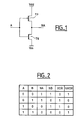
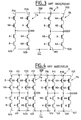
- the basic structure of a door OU-Exclusive realized using CMOS technology easily deduced from the basic structure of an inverter produced using this technology (FIG. 1) on the one hand, and the OR-Exclusive truth table (Figure 2) on the other hand.
- the basic inverter made in CMOS technology includes a P-type MOS transistor (referenced TP and comprising a small circle drawn on its control grid to distinguish it from a transistor of the other type) and a MOS transistor of type N (referenced TN) connected in series between two power terminals.
- the source of the transistor TP is connected to an upper supply terminal brought to a potential Vdd and its drain is connected to a node of exit.
- the source of the transistor TN is connected to a lower supply terminal brought to a potential Vss lower than Vdd or mass, and its drain is connected to the output node.
- Input signal A is focused on the common control grids of these two transistors.
- the output signal NA which is the complementary to input signal A is available on the exit node common to the drains of the two transistors.
- the P-type transistor ensures the switching of the output from logic state 0 to logic state 1 (edges output amounts, or transition 0-1).
- the transistor type N on the contrary ensures the switching of the output from logic state 1 to logic state 0 (edges descendants at exit, or transition 1-0).
- the Exclusive OR gate 11 then has two cells lla and 11b of identical structure but functioning symmetrically for, one, generate the XOR output at from inputs A, NA, B and NB and, the other, generate the additional NXOR output from the same starters.
- This structural identity and this symmetry in the operation contribute to obtaining a response time of the outputs which is independent of the couple of inputs A and NA or B and NB which switches, from nature of the 1-0 or 0-1 transition on those of XOR or NXOR outputs that we consider, and of the state logic of the pair of complementary inputs which not switch.
- the concept of symmetrical door is defined in the case of a door with four entrances complementary two by two and two outputs complementary by the characteristic of triple independence of the response time of the outputs such as stated above.
- OR-Exclusive door being for example intended to be used in a identical door shaft as described above, in which doors are connected in cascade there and advantageous that it generates itself on its outputs the complementary signals XOR and NXOR which constitute one of the pairs of complementary door entries of the next layer in the tree. This avoids the use of an inverter to generate the complementary of the XOR signal.
- FIG. 3 shows the basic structure of a Exclusive OU door with four complementary inputs two with two and two complementary outputs XOR and NXOR according to the prior art illustrated by the document EP-A-0 660 525.
- Each cell 11a and 11b has four branches: two P-type branches referenced P10 and P20, so called hereinafter because they include two P-type MOS transistors connected in series, which are connected in parallel between the terminal power supply and the output node of the cell; and two N-type branches referenced N10 and N20, so called hereinafter because they include two N-type MOS transistors connected in series, which are connected in parallel between the output node of the cubicle and the lower supply terminal.
- the two transistors of the same type of each branch are separated by an intermediate node.
- the control grids of the two transistors of each of the four branches P10, P20, N10, N20 of each cell exclusively receive one of the four input couples ⁇ A, B ⁇ , ⁇ NA, B ⁇ , ⁇ A, NB ⁇ , or ⁇ NA, NB ⁇ .
- a couple of transistors of a single branch receives any of the four pairs of entries above, and that each of these input pairs is assigned to the two transistors of only one of the four branches of the cell.
- the two P-type MOS transistors of the branch P10 respectively receive the inputs NA and B on their control grids while those of the branch P20 receive the two inputs A and NB, the two N type transistors of the N10 branch receiving respectively the two inputs A and B and those of the branch N20 receiving the two inputs NA and NB.
- the two transistors of type P of branch P10 receive the two inputs A and B on their order grids, while those of the branch P20 receive the two inputs NA and NB, the two N type transistors of the N10 branch receiving inputs A and NB and those of branch N20 receiving the two entries NA and B.
- the improvement comes from the modification of the door structure which consists in connecting, parallel on each branch of the door, another branch of the same type, called twin branch of said branch, whose transistors receive on their grid the reverse torque of the input torque received by the control grid of the transistors of said plugged.
- twin branch of said branch whose transistors receive on their grid the reverse torque of the input torque received by the control grid of the transistors of said plugged.
- the inverse couple of a couple of inputs any ⁇ X, Y ⁇ is defined as the pair ⁇ Y, X ⁇ .
- the notion of input couple is therefore a notion call to an order relation between said entries.
- a twin branch P11 is put in parallel on the P10 branch of each cell 11a or 11b, a twin branch P21 being placed in parallel on the P20 branch, while a branch N11 twin is put in parallel on the N10 branch and that a branch N21 is put in parallel on the branch N20, the two transistors of each twin branch receiving the inverse torque of the input torque received by the transistors of each of the branches to which they are associated.
- the impedance seen by each input is the impedance equivalent of a P-type transistor (the one close to the upper supply terminal) in parallel with two P-type transistors in series, all while parallel with the impedance of an N-type transistor, (the one near the lower power terminal) in parallel with two N type transistors.
- twin branches are arranged according to the invention so as to fill a new function which removes the floating character that the node can have intermediate of each of the branches.
- the two transistors of the branch N10 adjacent to branch N20 which is conductive, are non-conductive as receiving on their control grid for signals in logic state 0.
- the intermediate node of branch 10 is therefore floating.
- the transistor close to the upper power terminal which receives input B is conductive so that the potential on the middle node of this branch is substantially equal to the potential Vdd.
- the transistor close to the output node receiving input A which is conductive is the transistor close to the output node receiving input A which is conductive, so that the potential of the node intermediate of said branch is substantially equal at the potential of the cell output node, in the occurrence a potential close to Vss.
- the potential on the knot intermediate of branch N10 has an initial value depending on the previous state of the four A inputs, NA, B and NB.
- the potential on the intermediate node of the branch N10 is only maintained by the action of parasitic capacitances of the transistors, and in particular of the drain / substrate capacity (the substrate being brought to Vss potential for N type transistors and at Vdd potential for P type transistors). AT assume that the entries remain in the configuration considered for a sufficient period, this potential will fall due to leakage currents.
- the node intermediate should be charged to a near potential of Vdd (if it is the entry A which passed to the state logic 1) or discharged to a potential close to Vss (if it is the entry B which is passed back to the logical state 1) to starting from an initial potential whose value will depend the (indefinite) period during which the two inputs A and B remained in logic state 0.
- Vdd near potential of Vdd
- Vss potential close to Vss
- means making it possible to impose in all circumstances a potential on the nodes intermediaries of each branch are proposed. These means include the twin branches described above with reference to FIG. 4, but arranged with a new way allowing them to complete a new function, other than that of equalization of the impedance seen by each of the inputs.
- This arrangement according to the invention is visible in Figure 5.
- the intermediate node of any branches of a specific type (type P or type N) is connected to the intermediate node of the twin branch of the other branch of the same type of the same cell.
- the intermediate node of the branch P10 of type P is connected to the intermediate node of the branch P21 twin of the other P20 type P branch of the cell.
- the intermediate node of the branch P20 of type P is connected to the intermediate node of the twin branch P11 of the other branch P10 of type P of the cell.
- the intermediate node of branch N10 of type N is connected to the node intermediate of the twin branch N21 of the other N20 type N branch of the cell.
- the knot intermediate of branch N20 of type N is connected to the intermediate node of the twin branch N11 of the other N10 branch of type N of the cell.
- This intermediate node is the occurrence brought to a potential substantially equal to Vss, so that the intermediate node of branch N10 is discharged at potential Vss. More generally, we can show that the effect of connections between the node intermediary of a branch of a given type and the node intermediary of the twin branch of the other branch of the same type of the same cell, is to discharge the parasitic drain / substrate capacitance of the transistor branch adjacent to the conductive branch which is close to the power terminal. Indeed, for P-type branches this capacity connects the terminal upper supply and the intermediate node whereas, for the N type branches, it connects the lower power terminal and node intermediate.
- each of these new paths involves two transistors receiving on their control grid one of the four inputs and its input respectively complementary. So for example, always for the cell 11a, the N-type transistor of branch N10 which is located on the side of the output node receives the input A while the N type transistor of branch N21 located on the side of the lower power terminal receives the NA input, so the path created between the XOR output node and the power supply terminal lower across these two transistors is never driver.
- the impedance seen by each of the four entries is always the same, well that of value different from that seen by the four Entrances to the door of Figure 4 of the prior art.
- the Exclusive-OR door being produced in a single circuit integrated in CMOS technology, the width of the channel P-type transistors is 2.5 times greater than the channel width of type N transistors. so we compensate for the weak charging current P-type transistors compared to that of load current of N-type transistors, due to the difference in charge carrier mobility in one and the other type of transistor.
- This provision is planned so that the two outputs XOR and NXOR of door 11 commute substantially symmetrically simultaneously. This is particularly advantageous when the Exclusive OR gate is intended to be used in a tree of identical doors.
- the invention also relates to a multiplier of frequency of the type presented in the introduction to the present description, in which the door shaft OU-Exclusive is made with doors conforming to the figure 5. Note that it is necessary to generate the logical complementary signals of signals sampled which are applied at the entrance of the doors OU-Exclusive of the first layer of the tree. These complementary signals are also received by tree entrances. A means to generate these signals complementary without introducing a delay between the switching of a signal and that of its signal complementary is for example described in the document EP-A-0 660 525.
- the propagation times of fronts through the shaft of Ou-Exclusive doors are equalized, whatever the evolution of the logical state inputs, with an accuracy of around two picoseconds.
- the invention therefore provides a result substantial that could be verified.
Landscapes
- Physics & Mathematics (AREA)
- Engineering & Computer Science (AREA)
- Computer Hardware Design (AREA)
- Computing Systems (AREA)
- General Engineering & Computer Science (AREA)
- Mathematical Physics (AREA)
- Nonlinear Science (AREA)
- Logic Circuits (AREA)
Abstract
Description
- à la figure 1 : le schéma classique d'un inverseur réalisé en technologie CMOS ;
- à la figure 2 : la table de vérité de la fonction OU-Exclusif à quatre entrées complémentaires deux à deux et à deux sorties complémentaires ;
- à la figure 3 : la structure de base d'une porte OU-Exclusif à quatre entrées complémentaires deux à deux et à deux sorties complémentaires XOR et NXOR (art antérieur) ;
- à la figure 4 : la structure d'une telle porte modifiée de manière à la rendre symétrique (art antérieur) ;
- à la figure 5 : un mode de réalisation d'une porte OU-Exclusif selon l'invention.
- les grilles de commande des deux transistors de chacune des quatre branches de chaque cellule reçoivent exclusivement l'un des quatre couples d'entrées {A,B}, {NA,B}, {A,NB} ou {NA,NB};
- les deux branches d'une même cellule qui sont du même type (les branches P10 et P20 de type P, ou les branches N10 et N20 de type N) reçoivent des couples d'entrée complémentaires deux à deux (à titre d'exemple le couple {B,NA} et le couple {NB,A} pour les branches de type P de la première cellule 11a);
- les deux branches d'un type quelconque (par exemple de type P) d'une cellule déterminée (par exemple la cellule lla) reçoivent respectivement les deux même couples d'entrée que les deux branches de l'autre cellule (la cellule 11b) qui sont de l'autre type (de type N).
Claims (3)
- Porte OU-Exclusif à quatre entrées complémentaires deux à deux A et NA, et B et NB, et à deux sorties complémentaires XOR et NXOR, dans laquelle deux cellules (11a-11b) comportent chacune, connectées en parallèle, deux branches (P10, P20) d'un premier type (type P) comprenant chacune un premier et un second transistors MOS de type P connectés en série entre une borne d'alimentation supérieure et un noeud de sortie (XOR ou NXOR) et séparés par un noeud intermédiaire, et, également connectées en parallèle, deux branches (N10, N20) d'un second type (type N) comme comprenant chacune un premier et un second transistors MOS de type N connectés en série entre le noeud de sortie et une borne d'alimentation inférieure et séparés par un noeud intermédiaire ;caractérisé en ce que, en parallèle sur chaque branche (P10, P20, N10, et N20), est en outre connectée une branche de même type, dite branche jumelle (respectivement P11, P21, N11, et N21) de ladite branche, dont le premier et le second transistors reçoivent sur leur grille de commande le couple d'entrées inverse du couple d'entrées reçu par les grilles de commande des transistors de ladite branche ;les grilles de commande des deux transistors de chacune des quatre branches de chaque cellule recevant exclusivement l'un des quatre couples d'entrées {A,B}, {NA,B}, {A,NB}, ou {NA,NB} ;les deux branches d'une même cellule qui sont du même type recevant des couples d'entrées complémentaires deux à deux ;les deux branches d'un type quelconque (type P, resp. type N) d'une cellule déterminée recevant respectivement les deux mêmes couples d'entrées que les deux branches de l'autre cellule qui sont de l'autre type (type N, resp. type P),
et en ce que, dans chaque cellule, le noeud intermédiaire d'une quelconque des branches d'un type déterminé (type P ou type N) est relié au noeud intermédiaire de la branche jumelle de l'autre branche de même type. - Porte OU-Exclusif selon la revendication 1, caractérisée en ce que la largeur de canal des transistors MOS de type P est 2,5 fois plus grande que celle des transistors MOS de type N.
- Multiplieur de fréquence du type comprenant une chaíne de N circuits à retard pour générer N signaux d'échantillonnage déphasés dans le temps à partir d'un signal d'horloge de fréquence déterminée fo, des moyens d'échantillonnage d'un mot de N bits d'information à transmettre se présentant en série à l'aide desdits N signaux d'échantillonnage qui produisent N signaux échantillonnés, et un arbre de portes OU-Exclusif à quatre entrées complémentaires deux à deux et à deux sorties complémentaires recevant sur ses entrées lesdits N signaux échantillonnés et leurs complémentaires logiques,
caractérisé en ce que les portes OU-Exclusif de l'arbre sont des portes OU-Exclusif selon l'une des revendications 1 ou 2.
Applications Claiming Priority (2)
| Application Number | Priority Date | Filing Date | Title |
|---|---|---|---|
| FR9711956 | 1997-09-25 | ||
| FR9711956A FR2768872B1 (fr) | 1997-09-25 | 1997-09-25 | Porte logique ou-exclusif a quatre entrees complementaires deux a deux et a deux sorties complementaires, et multiplieur de frequence l'incorporant |
Publications (2)
| Publication Number | Publication Date |
|---|---|
| EP0905907A1 true EP0905907A1 (fr) | 1999-03-31 |
| EP0905907B1 EP0905907B1 (fr) | 2003-05-14 |
Family
ID=9511484
Family Applications (1)
| Application Number | Title | Priority Date | Filing Date |
|---|---|---|---|
| EP98402263A Expired - Lifetime EP0905907B1 (fr) | 1997-09-25 | 1998-09-14 | Porte logique OU-exclusif à quatre entrées complémentaires deux à deux et à deux sorties complémentaires, et multiplicateur de fréquence l'incorporant |
Country Status (4)
| Country | Link |
|---|---|
| US (1) | US6137309A (fr) |
| EP (1) | EP0905907B1 (fr) |
| DE (1) | DE69814552D1 (fr) |
| FR (1) | FR2768872B1 (fr) |
Cited By (1)
| Publication number | Priority date | Publication date | Assignee | Title |
|---|---|---|---|---|
| EP2575257A1 (fr) * | 2011-09-29 | 2013-04-03 | Elpida Memory, Inc. | Circuit logique et système de traitement de données comprenant le même |
Families Citing this family (10)
| Publication number | Priority date | Publication date | Assignee | Title |
|---|---|---|---|---|
| US6414519B1 (en) * | 2000-09-15 | 2002-07-02 | Applied Micro Circuits Corporation | Equal delay current-mode logic circuit |
| US6724221B2 (en) * | 2002-03-28 | 2004-04-20 | International Business Machines Corporation | Circuitry having exclusive-OR and latch function, and method therefor |
| US6566912B1 (en) * | 2002-04-30 | 2003-05-20 | Applied Micro Circuits Corporation | Integrated XOR/multiplexer for high speed phase detection |
| TWI281317B (en) * | 2005-03-07 | 2007-05-11 | Sunplus Technology Co Ltd | Self DC-bias high frequency logic gate, NAND gate, and NOR gate using the same |
| US7285986B2 (en) * | 2005-08-22 | 2007-10-23 | Micron Technology, Inc. | High speed, low power CMOS logic gate |
| US7242219B1 (en) * | 2005-09-08 | 2007-07-10 | Advanced Micro Devices, Inc. | Circuit for parity tree structure |
| US7725512B1 (en) * | 2006-04-26 | 2010-05-25 | Altera Corporation | Apparatus and method for performing multiple exclusive or operations using multiplication circuitry |
| US7557614B1 (en) * | 2008-07-15 | 2009-07-07 | International Business Machines Corporation | Topology for a n-way XOR/XNOR circuit |
| KR102276890B1 (ko) | 2014-08-14 | 2021-07-12 | 삼성전자주식회사 | 주파수 더블러 |
| US10756753B2 (en) * | 2018-10-25 | 2020-08-25 | Arm Limited | Data compressor logic circuit |
Citations (5)
| Publication number | Priority date | Publication date | Assignee | Title |
|---|---|---|---|---|
| JPS5765927A (en) * | 1980-10-13 | 1982-04-21 | Hitachi Ltd | Logical operation circuit |
| JPS61294934A (ja) * | 1985-06-21 | 1986-12-25 | Mitsubishi Electric Corp | 半導体装置およびデ−タ伝送路 |
| JPH05152936A (ja) * | 1991-11-29 | 1993-06-18 | Oki Electric Ind Co Ltd | 論理回路 |
| EP0660525A1 (fr) * | 1993-12-24 | 1995-06-28 | Bull S.A. | Arbre de portes logiques OU-Exclusif et multiplieur de fréquence l'incorporant |
| US5479112A (en) * | 1994-01-25 | 1995-12-26 | Texas Instruments Incorporated | Logic gate with matched output rise and fall times and method of construction |
-
1997
- 1997-09-25 FR FR9711956A patent/FR2768872B1/fr not_active Expired - Fee Related
-
1998
- 1998-09-14 EP EP98402263A patent/EP0905907B1/fr not_active Expired - Lifetime
- 1998-09-14 DE DE69814552T patent/DE69814552D1/de not_active Expired - Lifetime
- 1998-09-23 US US09/159,316 patent/US6137309A/en not_active Expired - Lifetime
Patent Citations (5)
| Publication number | Priority date | Publication date | Assignee | Title |
|---|---|---|---|---|
| JPS5765927A (en) * | 1980-10-13 | 1982-04-21 | Hitachi Ltd | Logical operation circuit |
| JPS61294934A (ja) * | 1985-06-21 | 1986-12-25 | Mitsubishi Electric Corp | 半導体装置およびデ−タ伝送路 |
| JPH05152936A (ja) * | 1991-11-29 | 1993-06-18 | Oki Electric Ind Co Ltd | 論理回路 |
| EP0660525A1 (fr) * | 1993-12-24 | 1995-06-28 | Bull S.A. | Arbre de portes logiques OU-Exclusif et multiplieur de fréquence l'incorporant |
| US5479112A (en) * | 1994-01-25 | 1995-12-26 | Texas Instruments Incorporated | Logic gate with matched output rise and fall times and method of construction |
Non-Patent Citations (4)
| Title |
|---|
| "cmos differential cascode exclusive or/nor circuits", IBM TECHNICAL DISCLOSURE BULLETIN., vol. 30, no. 9, February 1988 (1988-02-01), NEW YORK US, pages 17 - 19, XP002065281 * |
| PATENT ABSTRACTS OF JAPAN vol. 006, no. 144 (E - 122) 3 August 1982 (1982-08-03) * |
| PATENT ABSTRACTS OF JAPAN vol. 011, no. 161 (E - 509) 23 May 1987 (1987-05-23) * |
| PATENT ABSTRACTS OF JAPAN vol. 017, no. 542 (E - 1441) 29 September 1993 (1993-09-29) * |
Cited By (2)
| Publication number | Priority date | Publication date | Assignee | Title |
|---|---|---|---|---|
| EP2575257A1 (fr) * | 2011-09-29 | 2013-04-03 | Elpida Memory, Inc. | Circuit logique et système de traitement de données comprenant le même |
| US8773165B2 (en) | 2011-09-29 | 2014-07-08 | Elpida Memory, Inc. | Logic circuit performing exclusive or operation and data processing system including the same |
Also Published As
| Publication number | Publication date |
|---|---|
| FR2768872A1 (fr) | 1999-03-26 |
| US6137309A (en) | 2000-10-24 |
| EP0905907B1 (fr) | 2003-05-14 |
| DE69814552D1 (de) | 2003-06-18 |
| FR2768872B1 (fr) | 2000-09-08 |
Similar Documents
| Publication | Publication Date | Title |
|---|---|---|
| EP0660525B1 (fr) | Multiplieur de fréquence comportant un arbre de portes logiques OU-Exclusif de type CMOS | |
| EP0905907B1 (fr) | Porte logique OU-exclusif à quatre entrées complémentaires deux à deux et à deux sorties complémentaires, et multiplicateur de fréquence l'incorporant | |
| EP1863179A1 (fr) | Circuit décaleur de niveau | |
| FR2593652A1 (fr) | Reseau logique programmable a logique dynamique a horloge unique. | |
| FR2488006A1 (fr) | Circuit de report perfectionne pour un additionneur binaire | |
| EP0194195B1 (fr) | Bascule bistable statique en technologie CMOS | |
| EP3376670B1 (fr) | Ligne à retard configurable | |
| EP0006053A1 (fr) | Dispositif différentiel à transfert de charges électriques, filtre et ligne à retard comportant un tel dispositif | |
| EP0283393A1 (fr) | Dispositif de calcul binaire | |
| EP0229433B1 (fr) | Dispositif de test de circuit logique combinatoire | |
| WO2007000387A1 (fr) | Commutateur de courant a paire differentielle de transistors alimente par une faible tension vcc | |
| EP0309348A1 (fr) | Dispositif d'addition et de multiplication binaire | |
| FR2773020A1 (fr) | Circuit de distribution d'horloge dans un circuit integre | |
| EP0424222A1 (fr) | Circuit intégré logique, à temps de basculement réglable | |
| EP0065460B1 (fr) | Compteur parallèle en circuit intégré MOS et application à la réalisation d'un additionneur binaire | |
| FR2986679A1 (fr) | Generateur de nombres aleatoires vrais | |
| EP1845619A1 (fr) | Circuit tampon comprenant des moyens de contrôle de la pente du signal de sortie | |
| FR2573939A1 (fr) | Circuit multiplexeur de signaux integre a quatre voies d'entree | |
| EP0186533A1 (fr) | Elément de mémoire dynamique et son utilisation dans une bascule maître-esclave et dans des circuits séquentiels programmables | |
| FR2773652A1 (fr) | Circuit de generation d'un signal d'activation commande | |
| EP0687071A1 (fr) | Dispositif incluant un circuit à étages logiques dynamiques | |
| EP1322076A1 (fr) | Dispositif de commutation comportant des moyens de décodage local | |
| EP0027884B1 (fr) | Circuit comportant au moins deux dispositifs semi-conducteurs en technologie MTL présentant des temps de montée différents et circuits logiques en dérivant | |
| EP1777904B1 (fr) | Multiplexeur à haut débit à architecture parallèle | |
| EP0720173A1 (fr) | Element de memoire statique du type bascule latch |
Legal Events
| Date | Code | Title | Description |
|---|---|---|---|
| PUAI | Public reference made under article 153(3) epc to a published international application that has entered the european phase |
Free format text: ORIGINAL CODE: 0009012 |
|
| AK | Designated contracting states |
Kind code of ref document: A1 Designated state(s): DE FR GB IT |
|
| AX | Request for extension of the european patent |
Free format text: AL;LT;LV;MK;RO;SI |
|
| 17P | Request for examination filed |
Effective date: 19990518 |
|
| AKX | Designation fees paid |
Free format text: DE FR GB IT |
|
| RAP1 | Party data changed (applicant data changed or rights of an application transferred) |
Owner name: STMICROELECTRONICS S.A. |
|
| GRAH | Despatch of communication of intention to grant a patent |
Free format text: ORIGINAL CODE: EPIDOS IGRA |
|
| GRAH | Despatch of communication of intention to grant a patent |
Free format text: ORIGINAL CODE: EPIDOS IGRA |
|
| GRAA | (expected) grant |
Free format text: ORIGINAL CODE: 0009210 |
|
| AK | Designated contracting states |
Designated state(s): DE FR GB IT |
|
| PG25 | Lapsed in a contracting state [announced via postgrant information from national office to epo] |
Ref country code: IT Free format text: LAPSE BECAUSE OF FAILURE TO SUBMIT A TRANSLATION OF THE DESCRIPTION OR TO PAY THE FEE WITHIN THE PRESCRIBED TIME-LIMIT;WARNING: LAPSES OF ITALIAN PATENTS WITH EFFECTIVE DATE BEFORE 2007 MAY HAVE OCCURRED AT ANY TIME BEFORE 2007. THE CORRECT EFFECTIVE DATE MAY BE DIFFERENT FROM THE ONE RECORDED. Effective date: 20030514 |
|
| REG | Reference to a national code |
Ref country code: GB Ref legal event code: FG4D Free format text: NOT ENGLISH |
|
| RIN1 | Information on inventor provided before grant (corrected) |
Inventor name: COUTEAUX, PASCAL Inventor name: MARBOT, ROLAND |
|
| REF | Corresponds to: |
Ref document number: 69814552 Country of ref document: DE Date of ref document: 20030618 Kind code of ref document: P |
|
| GBT | Gb: translation of ep patent filed (gb section 77(6)(a)/1977) | ||
| PG25 | Lapsed in a contracting state [announced via postgrant information from national office to epo] |
Ref country code: DE Free format text: LAPSE BECAUSE OF FAILURE TO SUBMIT A TRANSLATION OF THE DESCRIPTION OR TO PAY THE FEE WITHIN THE PRESCRIBED TIME-LIMIT Effective date: 20030815 |
|
| PGFP | Annual fee paid to national office [announced via postgrant information from national office to epo] |
Ref country code: DE Payment date: 20030925 Year of fee payment: 6 |
|
| PLBE | No opposition filed within time limit |
Free format text: ORIGINAL CODE: 0009261 |
|
| STAA | Information on the status of an ep patent application or granted ep patent |
Free format text: STATUS: NO OPPOSITION FILED WITHIN TIME LIMIT |
|
| 26N | No opposition filed |
Effective date: 20040217 |
|
| PGFP | Annual fee paid to national office [announced via postgrant information from national office to epo] |
Ref country code: GB Payment date: 20060905 Year of fee payment: 9 |
|
| GBPC | Gb: european patent ceased through non-payment of renewal fee |
Effective date: 20070914 |
|
| REG | Reference to a national code |
Ref country code: FR Ref legal event code: ST Effective date: 20080531 |
|
| PG25 | Lapsed in a contracting state [announced via postgrant information from national office to epo] |
Ref country code: FR Free format text: LAPSE BECAUSE OF NON-PAYMENT OF DUE FEES Effective date: 20071001 |
|
| PGFP | Annual fee paid to national office [announced via postgrant information from national office to epo] |
Ref country code: FR Payment date: 20060928 Year of fee payment: 9 |
|
| PG25 | Lapsed in a contracting state [announced via postgrant information from national office to epo] |
Ref country code: GB Free format text: LAPSE BECAUSE OF NON-PAYMENT OF DUE FEES Effective date: 20070914 |