EP0905909B1 - Phasenregelkreis und Verfahren zur Rückgewinnung eines Taktsignals - Google Patents
Phasenregelkreis und Verfahren zur Rückgewinnung eines Taktsignals Download PDFInfo
- Publication number
- EP0905909B1 EP0905909B1 EP98307792A EP98307792A EP0905909B1 EP 0905909 B1 EP0905909 B1 EP 0905909B1 EP 98307792 A EP98307792 A EP 98307792A EP 98307792 A EP98307792 A EP 98307792A EP 0905909 B1 EP0905909 B1 EP 0905909B1
- Authority
- EP
- European Patent Office
- Prior art keywords
- signal
- signals
- logic
- frequency
- clock signal
- Prior art date
- Legal status (The legal status is an assumption and is not a legal conclusion. Google has not performed a legal analysis and makes no representation as to the accuracy of the status listed.)
- Expired - Lifetime
Links
- 238000000034 method Methods 0.000 title claims description 8
- 239000003990 capacitor Substances 0.000 claims description 45
- 230000007704 transition Effects 0.000 claims description 17
- 230000008859 change Effects 0.000 claims description 11
- 238000007599 discharging Methods 0.000 claims description 11
- 230000004044 response Effects 0.000 claims description 11
- 230000003111 delayed effect Effects 0.000 claims description 7
- 230000003213 activating effect Effects 0.000 claims 2
- 230000000295 complement effect Effects 0.000 description 13
- 238000010586 diagram Methods 0.000 description 12
- 238000001514 detection method Methods 0.000 description 10
- 230000010355 oscillation Effects 0.000 description 9
- 238000012937 correction Methods 0.000 description 8
- 238000013459 approach Methods 0.000 description 7
- 230000000737 periodic effect Effects 0.000 description 7
- 238000010276 construction Methods 0.000 description 6
- 238000011084 recovery Methods 0.000 description 6
- 238000004891 communication Methods 0.000 description 3
- 230000001419 dependent effect Effects 0.000 description 3
- 230000008569 process Effects 0.000 description 3
- 239000013078 crystal Substances 0.000 description 2
- 238000013461 design Methods 0.000 description 2
- 238000000605 extraction Methods 0.000 description 2
- 238000012545 processing Methods 0.000 description 2
- 230000001902 propagating effect Effects 0.000 description 2
- 238000004904 shortening Methods 0.000 description 2
- 230000001960 triggered effect Effects 0.000 description 2
- 230000009471 action Effects 0.000 description 1
- 230000003321 amplification Effects 0.000 description 1
- 230000009286 beneficial effect Effects 0.000 description 1
- 230000008901 benefit Effects 0.000 description 1
- 230000003247 decreasing effect Effects 0.000 description 1
- 230000009977 dual effect Effects 0.000 description 1
- 230000000694 effects Effects 0.000 description 1
- 239000000835 fiber Substances 0.000 description 1
- 238000001914 filtration Methods 0.000 description 1
- 230000036039 immunity Effects 0.000 description 1
- 230000006872 improvement Effects 0.000 description 1
- 238000003199 nucleic acid amplification method Methods 0.000 description 1
- 238000005086 pumping Methods 0.000 description 1
- 230000000630 rising effect Effects 0.000 description 1
- 239000007787 solid Substances 0.000 description 1
Images


Classifications
-
- H—ELECTRICITY
- H04—ELECTRIC COMMUNICATION TECHNIQUE
- H04L—TRANSMISSION OF DIGITAL INFORMATION, e.g. TELEGRAPHIC COMMUNICATION
- H04L7/00—Arrangements for synchronising receiver with transmitter
- H04L7/02—Speed or phase control by the received code signals, the signals containing no special synchronisation information
- H04L7/033—Speed or phase control by the received code signals, the signals containing no special synchronisation information using the transitions of the received signal to control the phase of the synchronising-signal-generating means, e.g. using a phase-locked loop
-
- H—ELECTRICITY
- H03—ELECTRONIC CIRCUITRY
- H03L—AUTOMATIC CONTROL, STARTING, SYNCHRONISATION OR STABILISATION OF GENERATORS OF ELECTRONIC OSCILLATIONS OR PULSES
- H03L7/00—Automatic control of frequency or phase; Synchronisation
- H03L7/06—Automatic control of frequency or phase; Synchronisation using a reference signal applied to a frequency- or phase-locked loop
- H03L7/08—Details of the phase-locked loop
- H03L7/085—Details of the phase-locked loop concerning mainly the frequency- or phase-detection arrangement including the filtering or amplification of its output signal
- H03L7/089—Details of the phase-locked loop concerning mainly the frequency- or phase-detection arrangement including the filtering or amplification of its output signal the phase or frequency detector generating up-down pulses
- H03L7/0891—Details of the phase-locked loop concerning mainly the frequency- or phase-detection arrangement including the filtering or amplification of its output signal the phase or frequency detector generating up-down pulses the up-down pulses controlling source and sink current generators, e.g. a charge pump
-
- H—ELECTRICITY
- H03—ELECTRONIC CIRCUITRY
- H03L—AUTOMATIC CONTROL, STARTING, SYNCHRONISATION OR STABILISATION OF GENERATORS OF ELECTRONIC OSCILLATIONS OR PULSES
- H03L7/00—Automatic control of frequency or phase; Synchronisation
- H03L7/06—Automatic control of frequency or phase; Synchronisation using a reference signal applied to a frequency- or phase-locked loop
- H03L7/08—Details of the phase-locked loop
- H03L7/099—Details of the phase-locked loop concerning mainly the controlled oscillator of the loop
- H03L7/0995—Details of the phase-locked loop concerning mainly the controlled oscillator of the loop the oscillator comprising a ring oscillator
Definitions
- This invention is generally related to the field of phase-locked loops for data communications circuits.
- clock recovery As is well known in the art, the receipt of communicated digital signals in modern communication systems, whether for voice, video, or data, often requires the generation of a clock signal from the received digital signals.
- This process of clock generation particularly from a data bitstream in which the logic states vary from cycle to cycle, is referred to in the art as “clock recovery” or “clock extraction”.
- the clock signal that is recovered from the input signal stream is conventionally used to synchronize receiver-end signal processing circuitry with the incoming signal.
- phase-locked loops are generally used to recover a clock signal from an incoming bit stream.
- PLLs typically include a phase/frequency detector that compares the incoming signal against the current state of a generated clock signal, and generates a voltage in response to the phase relationship between the two. The voltage is applied, after filtering (e.g., by charge-pumping a capacitor in a low-pass filter) and amplification as desired, to a voltage-controlled oscillator (VCO). The VCO generates the clock signal at a frequency that varies with the voltage from the phase/frequency detector, and forwards this clock signal to the processing circuitry and to the phase/frequency detector. As the frequency and phase of the clock signal approach that of the incoming bit stream, the PLL operation stabilizes at a steady state (i.e., a "locked" condition).
- PLL design and functionality is relatively straightforward when the input signal is itself periodic.
- PLL synchronization with an input bitstream of varying data is somewhat more complex, as the input signal is not strictly periodic but will, of course, depend upon the actual data being communicated. For example, assuming a duty cycle of the order of 50%, an input bitstream of all "1" states will appear as a periodic signal of the maximum frequency; conversely, an input bitstream of random (from the viewpoint of the PLL) "0" and "1" states will not be strictly periodic, but will appear as cycles of varying frequency.
- the clock recovery circuitry must, be capable of both locking onto such an input bitstream and maintaining a relatively steady output clock signal.
- the charge and discharge pulses are dependent upon the input data pattern, and not merely its frequency; it is believed that this dependence will cause pull-out even at a small frequency difference especially if a series of "1" level bits are received.
- the capacitor is charged and discharged in a discontinuous fashion according to this approach, resulting both in a relatively slow “pull-in” (or “lock-in”) time from a large error frequency, and also in uncontrollable jitter at small error frequencies.
- Rotational frequency detector Another conventional clock recovery approach, referred to as a "rotational frequency detector", is described in Wolaver, Phase-Locked Loop Circuit Design (Prentice Hall, 1991), pp. 177-183.
- the rotational frequency detector relies upon a comparison of the input signal to fundamental and quadrature phases of the recovered clock signal to determine which one of four possible phase relationship "quadrants" corresponds to each edge of the input signal.
- the direction i.e., clockwise or counterclockwise
- the input frequency indicates whether the input frequency is greater or less than that of the recovered clock.
- the rotational frequency detector similarly as the Pottbburger approach, charges and discharges the low-pass filter capacitor discontinuously, again resulting in long pull-in times and also jitter. Furthermore, it is apparent from the Wolaver reference that the rotational frequency detector is relatively inefficient in detecting clock slips, and also in utilizing all available rotational information; these inefficiencies are reflected in clock signal inaccuracies and also in long response times.
- EP 0458269 A1 disloses a phase-locked loop circuit comprising a controller for driving a low-pass filter continually in response to a signal from a phase-comparator which compares a divided frequency of an oscillation frequency with a reference frequency.
- the phase-locked loop circuit includes a lock-up time shortening circuit.
- the latter includes a sequential logic controlling the charge pump circuit in response to the up/down signals from the phase comparator. As soon as an overshoot is detected in the low-pass filter output, which means that the latter exceeds a predetermined lock-up voltage, the lock-up time shortening circuit is desactivated.
- the present invention provides a frequency/phase detector in which lock-in time is minimized.
- the present invention further provides a frequency/phase detector in which lock-in accuracy in combination with small lock-in time.
- the present invention yet further provides a frequency/phase detector which is not dependent upon the incoming data states in reaching lock-in.
- the present invention also provides a phase-locked loop circuit having such a frequency/phase detector.
- the present invention may be implemented into a phase-locked loop integrated circuit having a charge pump circuit for charging and discharging a capacitor in response to a frequency/phase detector circuit.
- the capacitor voltage is applied to an input of a voltage controlled oscillator to generate the recovered clock.
- the frequency/phase detector is realized as a state machine that receives logic signals corresponding to the relationship of the input signal to fundamental and quadrature phases of the output recovered clock signal.
- the state machine detects the rotational direction of a large error frequency and controls a charge pump to rapidly modulate the output clock frequency in response to the detected direction, until a change in rotational direction is detected. Once the change in rotational direction is detected, slower modulation of the clock frequency is effected responsive to the detected phase relationship of the input signal and the recovered clock.
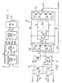
- phase-locked loop circuit Referring first to Figure 1, an example of a phase-locked loop circuit will be described.
- the phase-locked loop circuit of Figure 1 is particularly useful for implementation into a single integrated circuit either as a stand-alone circuit or, alternatively, in combination with other functionality such as that implemented into modern VLSI devices.
- the phase-locked loop circuit may be implemented as "front-end" circuitry within a high performance microprocessor, such as a digital signal processor (DSP).
- DSP digital signal processor
- the phase-locked loop may be realized as a combination of multiple discrete integrated circuits, if desired.
- the phase-locked loop includes frequency/phase detector circuit 10, charge pump filter 20, and voltage controlled oscillator (VCO) 30, connected in sequence.
- frequency/phase detector circuit 10 receives an input bitstream on line IN in combination with a clock signal on line CLK from the output of VCO 30; the clock signal on line CLK is a clock signal that is being generated, or "recovered", from the input bitstream on line IN.
- Frequency/phase detector circuit 10 includes fundamental/quadrature phase comparator circuit 12 for comparing the phase of the input bitstream to both fundamental and quadrature phases of the recovered clock signal on line CLK.
- Frequency/phase detector circuit 10 communicates the result of this comparison on lines A, C to state machine 14, as illustrated in Figure 1.
- state machine 14 Based on the phase relationship of the input signal to the recovered clock in a current cycle and in preceding cycles, state machine 14 generates signals on lines UPC, UPD, DND, DNC that are applied to charge pump filter 20 on lines V p , V n .
- Charge pump filter 20 is a low-pass filter including a capacitor that is controllably charged and discharged in response to the signals on lines UPC, UPD, DND, DNC from state machine 14. The voltage on this capacitor is applied (either individually or in combination with a second voltage derived therefrom) to VCO 30 which, in turn, generates a periodic signal on line CLK.
- the frequency of the signal on line CLK depends upon the magnitude of the voltage applied to VCO 30 by state machine 14. This signal on line CLK is applied as a feedback signal to frequency/phase detector circuit 10, for use in the frequency and phase comparison performed thereby.
- the a signal on one of lines UPC, DNC charges or discharges, as the case may be, the capacitor in charge pump filter 20 in a high-gain manner during the initial stages of lock-in.
- the selection of whether to charge or discharge the capacitor is controlled by frequency/phase detector circuit 10, and depends upon the rotational direction of the phase relationship between the input bitstream on line IN and the recovered clock signal on line CLK.
- the recovered clock signal on line CLK is generated by VCO 30 responsive to the output of charge pump filter 20.
- the recovered clock signal on line CLK is coarsely locked-in to the input frequency, as indicated by a change in the rotational direction of the input/output phase relationship, state machine 14 will generate signals on one or both of lines UPD, DPD to charge and discharge, respectively, the capacitor in charge pump filter 20 at a significantly slower rate, to achieve and maintain both frequency and phase lock-in. Accordingly, the clock signal on line CLK is a periodic signal that is "recovered”, or "extracted", from the input bitstream on line IN.
- charge pump filter 20 and VCO 30 Referring now to Figure 2, the detailed construction and interconnection of charge pump filter 20 and VCO 30 will now be described. Of course, other realizations of charge pump filter 20 and VCO 30 may be utilized.
- Charge pump filter 20 includes, as noted above, capacitor 25 which has one plate biased to ground.
- the other plate of capacitor 25, at node V n in Figure 2 is controllably charged and discharged by transistors 22p, 22n, 24p, 24n.
- Transistors 22p, 22n, 24p, 24n have their gates controlled by the voltage on lines UPD, DND, UPC, DNC, respectively, each of which is generated by state machine 14 to establish and modulate the voltage on capacitor 25 at node V n .
- transistors 22p, 24p have their sources biased to power supply voltage V dd
- n-channel transistors 22n, 24n have their sources at ground
- the drains of transistors 22p, 22n, 24p, 24n are all connected together to capacitor 25 at node V n .
- Additional series transistors for example with their gates biased to their drains, may be included in each leg of charge pump filter 20, to control conduction through transistors 22, 24, as is known.
- Transistors 22p, 24p are each operable to charge capacitor 25 and raise the voltage at node V n when turned "ON”, while transistors 22n, 24n are each operable to discharge capacitor 25 and lower the voltage at node V n when turned "ON".
- transistors 22p, 22n are substantially weaker in their drive capability than are transistors 24p, 24n.
- the gain of transistors 24p, 24n (preferably determined by their channel width/length ratio) may be significantly larger, such as ten times larger, than the gain of transistors 22p, 22n, respectively.
- This relationship permits lines UPC, DNC, when driven active, to rapidly charge and discharge, respectively, capacitor 25, and lines UPD, DND, when active, to slowly charge and discharge, respectively, capacitor 25.
- the dual rate of control of the voltage at node V n provides rapid and accurate lock-in of the phase-locked loop.
- Capacitor 25 is connected, also at node V n , to the gate of n-channel pull-down transistor 28.
- Transistor 28n has its source at ground, and its drain connected to the drain and gate of p-channel transistor 28p at node V p ; the source of transistor 28p is connected to power supply voltage V dd .
- the voltage at node V p will follow the voltage at node V n , such that the voltage at node V p will fall as the voltage at node V n rises, and vice versa.
- VCO 30 is arranged as an odd-numbered series of inverters 32 0 through 32 n (i.e., n being even), the switching times of each of which are controlled by the voltages at nodes V p , V n from charge pump filter 20.
- the input of each of inverters 32 is connected to the output of the preceding inverter, with the exception of inverter 32 0 which receives the output clock signal on line CLK at its input.
- VCO 30 operates substantially as a ring oscillator, with a frequency set by the switching times of inverters 32, and thus by the voltages on lines V p , V n driven by charge pump filter 20.
- inverter 32 0 includes p-channel transistor 34p and n-channel transistor 34n, the gates of which receive the state of line CLK (from inverter 32 n ).
- Inverter 32 0 also includes p-channel transistor 36, with its gate receiving the voltage at node V p , and n-channel transistor 38, with its gate receiving the voltage at node V n .
- the source/drain paths of transistors 34p, 36, 38, 34n are connected in series between power supply voltage V dd and ground.
- Output node Q 0 of inverter 32 0 is at the common drain connection between transistors 36, 38, and is driven to the logical complement of the state of line CLK at the gates of transistors 34p, 34n.
- the switching time of inverter 32 0 will depend upon the voltages at nodes V n , V p . For example, a relatively high voltage at node V n will render transistor 38 relatively conductive; this voltage will pull node V p relatively low, which will also render transistor 36 relatively conductive. With transistors 36, 38 turned “ON” relatively hard (i.e., having relatively little source/drain resistance), the switching time of inverter 32 0 will be relatively fast, but with transistors 36, 38 turned “ON” relatively slightly (i.e., having more source/drain resistance), the switching time of inverter 32 0 will be relatively slow.
- each of the remaining inverters 32 1 through 32 n in VCO 30 are similarly constructed and operate similarly as inverter 32 0 .
- each inverter 32 i in VCO 30 has an input, at the gates of transistors 34p, 34n therein, that receives output node Q i-1 from preceding inverter 32 i-1 , and drives output node Q i at the drains of its transistors 36, 38 to a complementary state from that at its input.
- series transistors 36, 38 are controlled by the voltages at nodes V p , V n , respectively, so that the switching time of each inverter 32 is controlled in the manner described above for inverter 32 0 .
- frequency/phase detector 10 controls the charging and discharging of capacitor 25, and thus the frequency of the clock signal on line CLK, in a particularly beneficial manner to obtain fast and accurate frequency lock-in.
- Figure 3 illustrates an example of an input bitstream on line IN and its relationship with an example of a recovered clock signal on line CLK; in this example, the input bitstream on line IN corresponds to a series of "1" data states, and as such approximates a periodic signal.
- the clock signal on line CLK corresponds to a fundamental phase;
- Figure 3 also illustrates, on line CLKQ, a quadrature phase (i.e., 90° lagging phase) of the clock signal on line CLK.
- logic signals I1, I2 are generated by fundamental/quadrature phase comparator circuit 12 to correspond to the logic level of the clock signal on lines CLK, CLKQ, respectively, at the time of an edge (either rising or falling) of the input signal on line IN.
- Figure 3 illustrates a series of logic levels for each of logic signals I1, I2 for the pulses of clock signals on line IN, CLK, CLKQ that are also illustrated therein.
- the compared clocks are the clock signal on line CLK and the input signal on line IN.
- Figure 4 illustrates the quadrants associated with the paired values of logic signals I1, I2 corresponding to the states of the fundamental and quadrature phase of the clock signal on lines CLK, CLKQ, respectively, with each edge of the signal on line IN.
- fundamental/quadrature phase comparator circuit 12 includes a pair of double-edge-triggered D-type latches 40, 42, each of which receives line IN at its clock input.
- Latch 40 receives line CLK at its D input and generates logic signal I1 at its Q output;
- latch 42 receives, at its D input, signal CLKQ which is generated from line CLK via 90° delay stage 41, and generates logic signal I2 at its Q output.
- Logic signals I1, I2, as generated by latches 40, 42, respectively, are applied to inputs of compare logic 44, along with logic signals on lines X1, X2 from next state logic 46, which correspond to the state of logic signals I1, I2 from a prior edge of the signal on line IN, as will be described hereinbelow.
- Compare logic 44 generates the results of the comparison of logic signals I1, I2 as generated from the most recent edge of the input signal on line IN with logic signals X1, X2, to determine if the progression is in a clockwise or anticlockwise direction.
- Compare logic 44 communicates the results of its comparison to state machine 14 on lines A, C; next state logic 46 also receives the state of lines A, C, as well as the state on line B and other signals from compare logic 44, based upon which it generates the next state signals on lines X1, X2 for application to compare logic 44 for the next input signal edge.
- Fundamental/quadrature phase comparator circuit 12 also includes initialization circuit 48, which generates initial states of logic signals I1, I2, X1, X2 before a recovered clock signal on line CLK has been generated.
- Initialization circuit 48 simply initializes lines I1, I2, X1, X2 to arbitrary states, from which rotation of the frequency relationship on lines CLK and IN may be detected. For example, lines X1, X2 may be initialized to a "0" state and lines I1, I2 to a "1" state, corresponding to a diagonal frequency relationship rotation.
- compare logic 44 generates signals on lines A, C, B to indicate anticlockwise, clockwise, and diagonal rotations, respectively, according to the convention illustrated in Figure 4.
- the signals on lines A, C will control state machine 14, which in turn will control the operation of charge pump filter 20 and VCO 30 to generate the recovered clock signal on line CLK.
- the diagonal signal on line B will be used by next state logic 46 to derive logic signals X1, X2 for the next edge of the signal on line IN.
- compare logic 44 receives logic signals I1, I2, X1, X2 at inputs of exclusive-OR gates 60A, 62A, 60C, 62C, and at inputs of exclusive-NOR gates 60B, 62B.
- exclusive-OR gate 60A receives logic signal I1 and the complement of logic signal X2 (from an inverter 61) at its inputs
- exclusive-OR gate 62A receives logic signals I2, X1 at its inputs
- exclusive-OR gate 60C receives logic signals I1, X2 at its inputs
- exclusive-OR gate 62C receives logic signal I2 and the complement of logic signal X1 (from an inverter 61).
- exclusive OR gates 60A, 62A are applied to NOR gate 64A, which has its output in turn connected to the D input of double-edge-triggered latch 66A; similarly, the outputs of gates 60C, 62C are applied to inputs of NOR gate 64C, the output of which is connected to the D input of latch 66C.
- Exclusive-NOR gate 60B receives logic signals I1, X1 at its inputs
- exclusive-NOR gate 62B receives logic signals I2, X2 at its inputs; the outputs of gates 60B, 62B are applied to inputs of NOR gate 64B, the output of which is connected to the D input of latch 66B.
- Latches 66A, 66C, 66B are all clocked by clocked edges on line IN, after delay by delay stage 63 so as to permit the generation and propagation of the input signals on lines I1, I2.
- Latch 66A drives the signal on line A at its Q output
- latch 66C drives line C with its Q output
- latch 66B drives line B with its Q output, each upon clocking by the delayed edge of the input signal on line IN.
- compare logic 44 receives the current edge logic signals I1, I2, and the previous edge logic signals X1, X2, and performs the logical combinations indicated by gates 60, 62, 64.
- the output of NOR gate 64A will be high responsive to logic signal I1 being at the same state as the complement of logic signal X2, in combination with logic signal I2 being at the same state as logic signal X1; in this event, the outputs of both of exclusive-OR gates 60A, 62A will be low, causing the output of NOR gate 64A to be high.
- This state will be clocked into latch 66A upon the delayed edge of the input signal on line IN, after which gate 66A will drive line A high, indicating an anticlockwise rotation (see Figure 4). It is contemplated that those of ordinary skill in the art will comprehend the operation of compare logic 44 for the other progressions indicated hereinabove, and as such specific description of such operation will be omitted from this description.
- next state logic 46 certain ones of the signals applied to gates 60, 62 are forwarded to next state logic 46. It is of course contemplated that one may simply store the current states of logic signals I1, I2 in latches, for use as logic signals X1, X2 in combination with the next edge of the input signal. However, given the high data rates and frequencies at which fundamental/quadrature phase comparison circuit 12 is required to operate, including up to on the order of GHz, direct generation of next state of logic signals X1, X2 from the current state logic signals X1, X2 is preferred.
- Next state logic 46 is arranged as groups of pass gates 68, 70, for passing a selected input state as logic signals X1, X2, respectively.
- Each of pass gates 68, 70 is constructed as a CMOS pass gate, having parallel p-channel and n-channel transistors controlled by complementary signals (inverted states generated by inverters 71 in next state logic 46).
- pass gate 68A receives signal O1A (which corresponds to X2 , the complement of logic signal X2) from one input of exclusive-OR gate 60A, and is controlled by anticlockwise signal A.
- pass gate 68C receives signal O1C (corresponding to logic signal X2) from the input of exclusive-OR gate 60C, and is controlled by clockwise signal C.
- Pass gate 68E receives X1 , the complement of logic signal X1, and is controlled by diagonal signal E.
- Signal E is generated by AND gate 69, which receives diagonal logic signal B at one input, and the output of NOR gate 67 at the other input.
- NOR gate 67 receives clockwise and anticlockwise signals C, A at its inputs; as a result, diagonal signal E is active responsive to diagonal signal B active in combination with both of anticlockwise and clockwise signals A, C, respectively, being inactive.
- the output sides of pass gates 68A, 68C, 68E are connected together in wired-OR fashion, and drive logic signal X1.
- logic signal X2 is generated substantially identically as logic signal X1 by way of pass gates 70A, 70C, 70E.
- Pass gate 70A receives signal O2A (i.e., logic signal X1) and is controlled by anticlockwise signal A
- pass gate 70C receives signal O2C (i.e., X1 ) and is controlled by clockwise signal C
- pass gate 70E receives signal X2 and is controlled by diagonal signal E.
- next state logic 46 in generating logic signals X1, X2 from its previous values will be readily apparent to the skilled reader.
- the logic signals X1, X2 are identical to the current input signals I1, I2, considering that the corresponding exclusive-OR gates have low level outputs (indicating equality at the inputs) in those cases.
- logic signals X1, X2 are simply inverted from the prior state. As such, logic signals X1, X2 are rapidly generated in such a manner as to avoid latching of the current logic signals I1, I2, enabling robust operation at high data rates.
- fundamental/quadrature phase comparator circuit 12 thus generates signals on lines A, C that indicate whether an anticlockwise or clockwise rotation of the phase relationship between the input signal on line IN and the recovered clock signal on line CLK has been detected.
- State machine 14 receives lines A, C and, based upon the current state and history of lines A, C, generates signals on one of lines UPC, UPD, DND, DNC that are applied to and control charge pump filter 20.
- State machine 14 includes sequential logic for generating these signals in a manner that will now be described in detail relative to Figure 8.
- Figure 8 is a state diagram illustrating the operation of state machine 14 in generating charge pump control signals on lines UPC, UPD, DND, DNC. It is contemplated that one of ordinary skill in the art, having reference to this description, will be readily able to realize the construction of state machine 14.
- State 72 is an initialization stage in which state machine 14 resides prior to lock-in of the recovered clock signal from the input bitstream.
- initialization circuitry 48 initializes the states of lines X1, X2, I1, I2; in addition, VCO 30 is preferably initialized by a local crystal oscillator to generate a signal on line CLK that is near the center of the lock-in range frequency range.
- State machine 14 remains in initialization state 72 until fundamental/quadrature phase comparator circuit 12 detects either an anticlockwise or clockwise phase relationship rotation, and indicates the same by an active state on lines A, C, respectively.
- state 74 is entered upon detection of an anticlockwise rotation, initiated by line A driven high.
- state machine 14 effects fast charging of capacitor 25 in charge pump filter 20 by asserting an active state on line UPC.
- the continuous charging of capacitor 25 effected by state machine 14 refers to the application of substantially a steady state active low level on line UPC, which turns "ON" p-channel transistor 24p to charge the plate of capacitor 25, at node V n , from power supply voltage V dd .
- lines UPD, DND, DNC are held inactive (line UPD high, and lines DND, DNC low), so that transistors 22p, 22n, 24n are turned “OFF”.
- This charging serves to rapidly increase the voltage on node V n and decrease the voltage on node V p , which in turn increases the frequency of the recovered clock signal on line CLK that is generated by VCO 30.
- the substantially steady state active low level on line UPC in state 74 may be effected simply by holding line UPC low, as will be described hereinbelow, or alternatively by pulsing line UPC to a low logic level at a relatively high duty cycle.
- Transition from state 74 only occurs upon detection of a clockwise phase relationship rotation, indicated by line C being driven active by fundamental/quadrature phase comparator circuit 12.
- state machine 14 makes a transition to state 80, as illustrated in Figure 8.
- the detection of a clockwise rotation after substantially continuous charging of charge pump filter 20 in state 74 indicates an overcorrection of the increase of the frequency of the recovered clock signal on line CLK, to a frequency greater than that of the input bitstream on line IN. Accordingly, in state 80, state machine 14 generates an active signal on line DND, which in this case is a high logic level, beginning the phase correction of the clock signal generated by VCO 30.
- this signal turns “ON” relatively weak transistor 22n with transistors 24p, 24n, 22p turned “OFF”, slowly discharging capacitor 25 toward ground, and reducing the voltage on node V n .
- This action slowly reduces the frequency of the recovered clock signal generated by VCO 30.
- state machine 14 remains in state 80 so long as no anticlockwise phase relationship rotations are detected (i.e., so long as only diagonal or additional clockwise rotations are detected).
- State machine 14 makes a transition from state 80 to state 76 upon detection of an anticlockwise rotation, as evidenced by an active state on line A.
- state machine 14 drives line UPD active (at a low logic level), which slowly charges capacitor 25 of charge pump filter 20 through weak transistor 22p, raising the voltage at node V n and slowly increasing the frequency of the recovered clock signal on line CLK.
- state machine 14 remains in fine correction states 76, 80 to correct for anticlockwise and clockwise phase rotations, respectively, with active signals applied to lines UPD, DND, as the case may be.
- state machine 14 As noted above, this construction of state machine 14 is provided by way of example only, as it is contemplated that those of ordinary skill in the art having reference to this specification will be readily able to implement state machine 14 in alternative realizations.
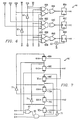
- NAND gates 82, 84 are received by state machine 14 at the inputs of NAND gates 82, 84, respectively.
- NAND gates 82, 84, along with NAND gates 86, 88, constitute combinational logic that operate upon the anticlockwise and clockwise signals on lines A, C in combination with the prior state of state machine 14 as indicated on lines Y1, Y2, Y3 at the outputs of D-type latches 92, 94, 96, respectively.
- NAND gate 82 also receives line Y3 at another input
- NAND gate 84 receives line Y2 and the complement of line Y3 at its other inputs.
- NAND gate 86 receives line Y1 and line Y2 at its inputs
- NAND gate 88 receives line Y1, the complement of line Y2, and line Y3 at its inputs.
- the outputs of NAND gates 82, 84, 86, 88 are applied to respective inputs of NAND gate 90, which drives the D input of latch 92 from its output.
- Latches 92, 94, 96 are all clocked by the logical OR of lines A, C (performed by OR gate 91), delayed by delay stage 93.
- Latch 94 receives line A at its D input
- latch 96 receives line C at its D input.
- latch 92 drives line Y1 to a level that is responsive to the logical combination performed by NAND gates 82, 84, 86, 88, 90 upon the current state of lines A, C and the prior state of state machine 14, while latches 94, 96 respectively drive lines Y2, Y3 with the state of lines A, C in this event.
- the states of lines Y1, Y2, Y3 at the outputs of latches 92, 94, 96, respectively, are used by state machine 14 to generate the control signals on lines UPC, UPD, DNC, DNC.
- AND gate 98 drives line UPC (via inverter 99, considering that line UPC drives p-channel transistor 24p in charge pump filter 20) responsive to the logical AND of line Y2 with the complements of lines Y1 and Y3.
- AND gate 102 drives line DNC with the logical AND of line Y3 with the complements of lines Y1 and Y2.
- AND gate 100 receives lines Y1, Y2 and the complement of line Y3 at its inputs, and drives line UPD with its output, after inversion by inverter 103 (considering that line UPD drives p-channel transistor 22p), and AND gate 104 receives lines Y1, Y3 and the complement of line Y2 at its inputs, and drives line DND at its output.
- lines UPC, DNC, UPD, DND are driven in a substantially continuous manner when the states of lines Y1, Y2, Y3 indicate the appropriate state.
- transistors 24 controlled by lines UPC, DNC are relatively strong relative to transistors 22 controlled by lines UPD, DND, and as such the rates of charging and discharging controlled by lines UPC, DNC are substantially larger than the rates controlled by lines UPD, DND.
- the charging and discharging of capacitor 25, and thus the control of VCO 30, may be effected in a continuous manner under the control of lines UPC, DNC, but in a discontinuous, or pulsed, manner under the control of lines UPD, DND (e.g., by including one-shot multivibrators at the output of AND gates 100, 104), to provide the different control rates.
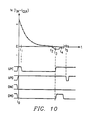
- the initial frequency of clock signal CLK is lower than that of the frequency of the input bitstream on line IN.
- the initial error frequency f e (which is the signed difference f IN -f CLK ) is positive.
- state machine 14 is in its initialized state 72.
- lines Y2, Y3 in state machine 14 are initialized to low logic levels (for example by way of a reset signal, not shown for clarity), with neither anticlockwise nor clockwise rotations having yet been detected.
- Line Y1 is initialized to a high logic level; the output from NAND gate 90 is initialized to a low logic level, however, considering that each of NAND gates 82, 84, 86, 88 receive at least one low logic level at their inputs (lines A, C, Y2, or Y3) and thus cause high logic levels at their outputs.
- VCO 30 is initialized, for example by way of a local crystal oscillator, to generate an initial clock signal on line CLK at a frequency that is preferably near the center of the frequency lock-in range. In this example, this initial frequency of line CLK is lower than that of the incoming bitstream on line IN.
- fundamental/quadrature phase comparator circuit 12 detects an anticlockwise rotation of the phase relationship between the signal on line CLK and the input bitstream on line IN. As noted above, in this event fundamental/quadrature phase comparator circuit 12 generates an active high level on line A, which is received by state machine 14.
- a high logic level on line A at time t 1 maintains NAND gate 82 in its same state, as line Y3 is initialized to a low level.
- each of latches 92, 94, 96 are clocked to store the levels at their respective inputs.
- latch 92 receives the low logic level output from NAND gate 90, and drives its output on line Y1 low.
- Latch 94 will receive the high logic level on line A and drive its output on line Y2 high; line Y1 line Y3 remains low, as line C is low at this time.
- the frequency of the clock signal on line CLK has reached the frequency of the input bitstream on line IN, as evident by the zero crossover of the error frequency f e .
- the frequency of the signal on line CLK continues to increase at this point, as line UPC remains at its active low level.
- fundamental/quadrature phase comparator circuit 12 detects a clockwise rotation of the phase relationship between the signal on line CLK and the input bitstream on line IN. As discussed above relative to Figures 3 and 4, a clockwise rotation can occur when the frequency on line CLK exceeds that of the input frequency. In response, fundamental/quadrature phase comparator circuit 12 generates an active level on line C, which is received by state machine 14 and causes a state transition.
- the high logic level on line C is received by NAND gate 84.
- This signal along with the high states of lines Y2 and the complement of line Y3, causes NAND gate 84 to drive a low logic level at its output, causing NAND gate 90 to in turn drive its output high.
- the high logic level on line C is latched by latch 96 and appears on line Y3, while the high logic level at the output of NAND gate 90 is latched by latch 92 and driven on line Y1; line Y2 is driven and held low at this time, as line A is low.
- fundamental/quadrature phase comparator circuit 12 detects an anticlockwise rotation of the phase relationship, and issues an active level on line A. This causes state machine 14 to make a transition from state 80 to state 76, (referring to Figure 8), and to generate an active (low) state on line UPD to charge capacitor 25 through weak transistor 22p (referring to Figure 2).
- this signal on line UPD is caused by the high level on line A being latched by latch 94 and driven on line Y2, in combination with the low level on line C being latched by latch 96 and driven on line Y3.
- the state of line Y1 remains high at this time, and at all times in states 76, 80, as at least one of NAND gates 86, 88 ensures that one low logic level is presented to one of the inputs of NAND gate 90.
- the signal on line UPD serves again to slowly raise the voltage at node V n in charge pump filter 20, slowly increasing the frequency of the clock signal on line CLK to approach the input bitstream frequency and phase on line IN.
- the frequency of the signal on line CLK approaches the input frequency and phase on line IN, the frequency of phase rotations (either clockwise or anticlockwise) will decrease.
- the time rate of change of the oscillation frequency of VCO 30 will decrease to a very low level.
- the recovered clock signal on line CLK may thus be considered as "locked-in" to the input bitstream frequency.
- the phase locked loop circuit thus provides the important benefit of being able to quickly achieve lock-in of the recovered clock signal from the input bitstream.
- This rapid lock-in is obtained primarily by rapid charging or discharging beginning from initialization, until such time as the output clock signal is detected as overcorrected. Once the first overcorrection has been detected, additional correction is made by slower charging or discharging of the charge pump capacitor, thus achieving fine correction of the frequency and phase relationship of the output clock signal to that of the input bitstream.
- phase-locked loop circuit will remain in the rapid charge/discharge mode for only on the order of ten cycles in locking in to a 100 MHz input frequency, following which the fine, phase, correction will result in lock-in after only about thirty to forty additional cycles. This performance is a significant improvement over conventional phase-locked loop circuits.
- phase-locked loop is contemplated to also minimize the amount of jitter at small error frequencies, particularly in comparison to conventional phase-locked loops.
- the improved lock-in performance is thus obtained without sacrificing accuracy or jitter.
- control of the charge pump may be carried out only upon receiving multiple instances of an anticlockwise or clockwise phase rotation (e.g., corresponding to two of the last three indications).
- multiple charge pump capacitors may be provided to carry out the coarse and fine corrections, as opposed to the single charge pump capacitor as used by the embodiment described hereinabove.
- the multiple charge pump capacitors may be of various sizes to accomplish charging and discharging of the VCO control voltage at different rates.
Landscapes
- Engineering & Computer Science (AREA)
- Computer Networks & Wireless Communication (AREA)
- Signal Processing (AREA)
- Stabilization Of Oscillater, Synchronisation, Frequency Synthesizers (AREA)
Claims (8)
- Phasenverriegelungsschleife, mit:einem spannungsgesteuerten Oszillator (30) zum Erzeugen eines Ausgangstaktsignals (CLK) mit einer von einer Steuerspannung (Vp, Vn) abhängenden Frequenz;einer Ladungspumpenschaltung (20) zum Erzeugen der Steuerspannung (Vp, Vn) in Reaktion auf ein erstes und ein zweites Ladungssteuersignal sowie auf ein erstes und ein zweites Entladungssteuersignal (UPC, UPD, DND, DNC); undeiner Frequenz/Phasen-Detektorschaltung (10), die umfasst:eine Phasenvergleichsschaltung (12) mit einem ersten Eingang zum Empfangen eines Eingangssignals (IN) und einem Rückkopplungseingang zum Empfangen des Ausgangstaktsignals (CLK), um ein erstes und ein zweites Indikatorsignal (A, C) zu erzeugen, die den von der Phasenvergleichsschaltung erfassten ersten bzw. zweiten Polaritäten einer Fehlfrequenz zwischen dem Eingangssignal und dem Ausgangstaktsignal entsprechen; undeine sequentielle Logik (14) zum Empfangen der Indikatorsignale (A, C) von der Phasenvergleichsschaltung (12) und zum Erzeugen eines ersten Ladungs-/Entladungssteuersignals (UPC; DNC) zum Steuern der Ladungspumpenschaltung, um die an den spannungsgesteuerten Oszillator angelegte Steuerspannung in Reaktion auf den Empfang eines ersten des ersten und des zweiten Indikatorsignals in einer ersten Richtung mit einer ersten Rate zu ändern, und dann zum Erzeugen eines zweiten Ladungs-/Entladungssteuersignals (UPD, DND) zum Steuern der Ladungspumpenschaltung (20), um die an den spannungsgesteuerten Oszillator angelegte Steuerspannung (Vp, Vn) in Reaktion auf den Empfang des anderen des ersten und des zweiten Indikatorsignals (A, C) in einer zweiten Richtung mit einer zweiten Rate, die niedriger als die erste Rate ist, zu ändern, wobei die Phasenvergleichsschaltung (12) ferner umfasst:eine Verzögerungsstufe (41) mit einem ersten Eingang zum Empfangen einer Grundphase des Ausgangstaktsignals (CLK) und zum Erzeugen einer Quadraturphase des Ausgangstaktsignals (CLKQ);eine Schaltungsanordnung (40, 42) zum Erzeugen eines Paars momentaner Logiksignale (I1, I2), die den Zuständen der Grundphase und der Quadraturphase des Ausgangstaktsignals entsprechen, in Reaktion auf den Empfang eines Übergangs des Eingangssignals; undeine Vergleichslogik (44) zum Vergleichen des Paars momentaner Logiksignale (I1, I2) mit einem Paar früherer Logiksignale (X1, X2), die Zuständen der Grundphase und der Quadraturphase des Ausgangstaktsignals bei einem früheren Übergang des Eingangssignals entsprechen, und zum Erzeugen von Signalen (A, C), die eine erste bzw. eine zweite Richtung angeben, in Reaktion auf die Richtung der Änderung der momentanen Logiksignale in Bezug auf die früheren Logiksignale in Übereinstimmung mit einer vorgegebenen Sequenz.
- Phasenverriegelungsschleife nach Anspruch 1, bei der die sequentielle Logik (14) so beschaffen ist, dass sie:wobei die sequentielle Logik (14) in Reaktion auf den Empfang einer ersten Instanz des die erste Richtung angebenden Signals von der Vergleichslogik (44) in den ersten Zustand eintritt und dort bleibt und in Reaktion auf den anschließenden Empfang des zweiten Indikatorsignals von der Vergleichslogik (44) in den vierten Zustand eintritt.in einem ersten Zustand ein Ladungssignal (UPC) mit hoher Verstärkung an die Ladungspumpenschaltung (20) anlegt;in einem zweiten Zustand ein Entladungssignal (DNC) mit hoher Verstärkung an die Ladungspumpenschaltung (20) anlegt;in einem dritten Zustand ein Ladungssignal (UPD) mit niedriger Verstärkung an die Ladungspumpenschaltung (20) anlegt; undin einem vierten Zustand ein Entladungssignal (DND) mit niedriger Verstärkung an die Ladungspumpenschaltung (20) anlegt;
- Phasenverriegelungsschleife nach Anspruch 1 oder Anspruch 2, bei der die Ladungspumpenschaltung (20) umfasst:einen ersten Transistor (24p), dessen Leitungspfad zwischen eine Stromversorgungsspannung und einen Kondensator (25) geschaltet ist und dessen Steuerelektrode so angeschlossen ist, dass sie das Ladungssignal (UPC) mit hoher Verstärkung empfängt;einen zweiten Transistor (22p), dessen Leitungspfad zwischen die Stromversorgungsspannung und den Kondensator (25) geschaltet ist und dessen Steuerelektrode so angeschlossen ist, dass sie das Ladungssignal (UPD) mit niedriger Verstärkung empfängt, wobei der zweite Transistor (22p) eine wesentlich schwächere Treibercharakteristik als der erste Transistor (24p) besitzt;einen dritten Transistor (24n), dessen Leitungspfad zwischen eine Referenzspannung und den Kondensator (25) geschaltet ist und dessen Steuerelektrode so angeschlossen ist, dass sie das Entladungssignal (DNC) mit hoher Verstärkung empfängt; undeinen vierten Transistor (22n), dessen Leitungspfad zwischen die Referenzspannung und den Kondensator (25) geschaltet ist und dessen Steuerelektrode so angeschlossen ist, dass sie das Entladungssignal (DND) mit niedriger Verstärkung empfängt, wobei der vierte Transistor (22n) eine wesentlich schwächere Treibercharakteristik als der dritte Transistor (24n) besitzt.
- Phasenverriegelungsschleife nach einem vorhergehenden Anspruch, bei dem die sequentielle Logik (14) umfasst:eine kombinatorische Logik (82, 84, 86, 88, 90) zum Empfangen der die erste bzw. die zweite Richtung angebenden Signale (A, C) und zum Empfangen mehrerer Rückkopplungssignale sowie zum Erzeugen eines Ausgangssignals, das angibt, ob die die erste bzw. die zweite Richtung angebenden Signale seit der Initialisierung empfangen worden sind;eine Verzögerungsschaltung (93) zum Erzeugen eines verzögerten Signals anhand des Auftritts entweder des die erste oder des die zweite Richtung angebenden Signals (A, C);einen ersten Zwischenspeicher (92) zum Speichern des Ausgangssignals der kombinatorischen Logik (82, 84, 86, 88, 90), der einen Takteingang besitzt, der das verzögerte Signal empfängt;einen zweiten und einen dritten Zwischenspeicher (94, 96) zum Speichern des Zustandes des die erste bzw. des die zweite Richtung angebenden Signals (A, C), wovon jeder einen Takteingang besitzt, der das verzögerte Signal empfängt; undeine Ausgangslogik (98, 99, 100, 102, 103, 104), die mit den Ausgängen des ersten, des zweiten und des dritten Zwischenspeichers (92, 94, 96) gekoppelt ist und das Ladungssignal und das Entladungssignal (UPC, DNC) mit hoher Verstärkung sowie das Ladungssignal und das Entladungssignal (UPD, DND) mit niedriger Verstärkung zu erzeugen.
- Verfahren zum Wiedergewinnen eines Taktsignals aus einem Eingangs-Bitstrom (IN), das die folgenden Schritte umfasst:wobei der Vergleichsschritt ferner umfasst:Initialisieren eines Ausgangstaktsignals (CLK) bei einer Anfangsfrequenz;periodisches Vergleichen des Eingangs-Bitstroms (IN) mit dem initialisierten Ausgangstaktsignal, um festzustellen, ob eine Frequenzbeziehung zwischen ihnen eine erste oder eine zweite Polarität hat;in Reaktion auf den Vergleichsschritt, wenn festgestellt wird, dass die Frequenzbeziehung die erste Polarität hat, Steuern des spannungsgesteuerten Oszillators (30) durch Aktivieren eines ersten des ersten und des zweiten Ladungssignals und des ersten und des zweiten Entladungssignals, um die Frequenz des Ausgangstaktsignals (CLK) in einer ersten Richtung mit einer ersten Rate zu ändern;anschließend in Reaktion auf den Vergleichsschritt, wenn festgestellt wird, dass die Frequenzbeziehung die zweite Polarität hat, Steuern des spannungsgesteuerten Oszillators (30) durch Aktivieren eines zweiten des ersten und des zweiten Ladungssignals und des ersten und des zweiten Entladungssignals, um die Frequenz des Ausgangstaktsignals (CLK) in einer zweiten, entgegen gesetzten Richtung mit einer zweiten Rate, die niedriger als die erste Rate ist, zu ändern,Erzeugen einer Quadraturphase des Ausgangstaktsignals (CLKQ) aus dessen Grundphase;in Reaktion auf jeden Übergang im Eingangs-Bitstrom (IN) Erzeugen eines Paars momentaner Logiksignale (I1, I2), die den Zustand der Grundphase und der Quadraturphase des Ausgangstaktsignals zum Zeitpunkt des Übergangs des Eingangs-Bitstroms (IN) entsprechen;Vergleichen des Paars momentaner Logiksignale (I1, I2) mit einem Paar früherer Logiksignale (X1, X2), wobei das Paar früherer Logiksignale (X1, X2) den Zustand der Grundphase bzw. der Quadraturphase des Ausgangstaktsignals zum Zeitpunkt eines früheren Übergangs des Eingangs-Bitstroms (IN) entspricht; .in Reaktion auf den Vergleichsschritt, bei dem eine Drehung der momentanen Logiksignale (I1, I2) gegenüber den früheren Logiksignalen (X1, X2) in einer ersten Richtung in einer vorgegebenen Sequenz erfasst wird, Ausgeben eines eine erste Richtung angebenden Signals (A); undin Reaktion auf den Vergleichsschritt, bei dem eine Drehung der momentanen Logiksignale (I1, I2) gegenüber den früheren Logiksignalen (I1, I2) in einer zweiten Richtung in der vorgegebenen Sequenz erfasst wird, Ausgeben eines eine zweite Richtung angebenden Signals (C).
- Verfahren nach Anspruch 5, das ferner umfasst:nach dem Schritt des Steuerns des spannungsgesteuerten Oszillators (30), um die Frequenz des Ausgangstaktsignals (CLK) in der zweiten Richtung zu ändern, Steuern des spannungsgesteuerten Oszillators (30), um die Frequenz des Ausgangstaktsignals (CLK) in der ersten Richtung mit einer zweiten Rate zu ändern, in Reaktion auf den Vergleichsschritt, wenn festgestellt wird, dass die Frequenzbeziehung die erste Polarität hat.
- Verfahren nach Anspruch 5 oder Anspruch 6, bei dem die Schritte des Steuerns des spannungsgesteuerten Oszillators (30) das wahlweise Laden und Entladen eines Kondensators (25) in einer Ladungspumpe (20) umfassen.
- Verfahren nach einem der Ansprüche 5 bis 7, bei dem der Schritt des Steuerns des spannungsgesteuerten Oszillators (30) in der ersten Richtung mit der ersten Rate das Durchschalten eines von mehreren Transistoren (24p, 24n) mit hoher Ansteuerung umfasst.
Applications Claiming Priority (2)
| Application Number | Priority Date | Filing Date | Title |
|---|---|---|---|
| US6034997P | 1997-09-29 | 1997-09-29 | |
| US60349P | 1997-09-29 |
Publications (3)
| Publication Number | Publication Date |
|---|---|
| EP0905909A2 EP0905909A2 (de) | 1999-03-31 |
| EP0905909A3 EP0905909A3 (de) | 2002-04-03 |
| EP0905909B1 true EP0905909B1 (de) | 2005-12-07 |
Family
ID=22028942
Family Applications (1)
| Application Number | Title | Priority Date | Filing Date |
|---|---|---|---|
| EP98307792A Expired - Lifetime EP0905909B1 (de) | 1997-09-29 | 1998-09-25 | Phasenregelkreis und Verfahren zur Rückgewinnung eines Taktsignals |
Country Status (3)
| Country | Link |
|---|---|
| US (1) | US6320921B1 (de) |
| EP (1) | EP0905909B1 (de) |
| DE (1) | DE69832674T2 (de) |
Families Citing this family (10)
| Publication number | Priority date | Publication date | Assignee | Title |
|---|---|---|---|---|
| GB2357382B (en) | 1999-12-17 | 2004-03-31 | Mitel Corp | Clock recovery PLL |
| US6510526B1 (en) * | 1999-12-23 | 2003-01-21 | Intel Corporation | Differential clocking for digital platforms |
| JP3502618B2 (ja) * | 2001-07-19 | 2004-03-02 | 松下電器産業株式会社 | 位相同期ループ回路、及びデータ再生装置 |
| US6763294B2 (en) * | 2002-05-06 | 2004-07-13 | Deere & Company | System and method for validating quadrature signals |
| US7245682B2 (en) * | 2002-09-30 | 2007-07-17 | Intel Corporation | Determining an optimal sampling clock |
| US6970020B1 (en) * | 2003-12-17 | 2005-11-29 | Altera Corporation | Half-rate linear quardrature phase detector for clock recovery |
| US8090064B2 (en) * | 2007-02-09 | 2012-01-03 | Fujitsu Limited | Single loop frequency and phase detection |
| CN111831965B (zh) * | 2019-04-23 | 2023-09-12 | 千寻位置网络有限公司 | Ssr中upd改正数的完好性监测方法及其装置 |
| CN111181552B (zh) * | 2020-01-08 | 2023-03-24 | 电子科技大学 | 一种双向频率同步振荡器电路 |
| CN116405058B (zh) * | 2023-06-09 | 2023-09-29 | 中星联华科技(北京)有限公司 | 快速跳频锁定电路及其运行方法 |
Family Cites Families (8)
| Publication number | Priority date | Publication date | Assignee | Title |
|---|---|---|---|---|
| DE69129946T2 (de) * | 1990-05-21 | 1999-04-15 | Nec Corp., Tokio/Tokyo | Phasenregelkreisschaltung |
| US5233314A (en) * | 1992-03-27 | 1993-08-03 | Cyrix Corporation | Integrated charge-pump phase-locked loop circuit |
| DE69535087T2 (de) * | 1994-03-11 | 2006-12-21 | Fujitsu Ltd., Kawasaki | Schaltungsanordnung zur Taktrückgewinnung |
| US5740213A (en) * | 1994-06-03 | 1998-04-14 | Dreyer; Stephen F. | Differential charge pump based phase locked loop or delay locked loop |
| US5850422A (en) * | 1995-07-21 | 1998-12-15 | Symbios, Inc. | Apparatus and method for recovering a clock signal which is embedded in an incoming data stream |
| KR100214503B1 (ko) * | 1996-09-02 | 1999-08-02 | 구본준 | 피에이엠방식 통신장치의 타이밍 복구회로 |
| US5870046A (en) * | 1997-04-22 | 1999-02-09 | Silicon Laboratories Inc. | Analog isolation system with digital communication across a capacitive barrier |
| US6127865A (en) * | 1997-05-23 | 2000-10-03 | Altera Corporation | Programmable logic device with logic signal delay compensated clock network |
-
1998
- 1998-09-25 EP EP98307792A patent/EP0905909B1/de not_active Expired - Lifetime
- 1998-09-25 DE DE69832674T patent/DE69832674T2/de not_active Expired - Lifetime
- 1998-09-25 US US09/160,905 patent/US6320921B1/en not_active Expired - Lifetime
Also Published As
| Publication number | Publication date |
|---|---|
| EP0905909A2 (de) | 1999-03-31 |
| US6320921B1 (en) | 2001-11-20 |
| DE69832674D1 (de) | 2006-01-12 |
| EP0905909A3 (de) | 2002-04-03 |
| DE69832674T2 (de) | 2006-07-20 |
Similar Documents
| Publication | Publication Date | Title |
|---|---|---|
| US8284887B2 (en) | Clock data recovery circuit and multiplied-frequency clock generation circuit | |
| US7719329B1 (en) | Phase-locked loop fast lock circuit and method | |
| US7302026B2 (en) | Clock recovery circuit and electronic device using a clock recovery circuit | |
| US6784707B2 (en) | Delay locked loop clock generator | |
| US7242733B2 (en) | Clock recovery circuit | |
| US7215207B2 (en) | Phase and frequency detection circuits for data communication systems | |
| JP2025128312A (ja) | デジタル-時間変換器 | |
| EP0866559A1 (de) | Phasenregelschleife | |
| US8040156B2 (en) | Lock detection circuit and lock detecting method | |
| US5276716A (en) | Bi-phase decoder phase-lock loop in CMOS | |
| US7668277B2 (en) | Apparatus and method for clock data recovery with low lock frequency | |
| EP0905909B1 (de) | Phasenregelkreis und Verfahren zur Rückgewinnung eines Taktsignals | |
| US6496046B2 (en) | Method for increasing the control bandwidth of a frequency control circuit | |
| EP3152761A1 (de) | Verzögerungsstruktur für eine speicherschnittstelle | |
| US20070205825A1 (en) | Switched Capacitor Filter And Feedback System | |
| EP3152762A1 (de) | Programmierbare leistung für eine speicherschnittstelle | |
| Cheng et al. | A difference detector PFD for low jitter PLL | |
| US8362817B2 (en) | Phase comparator and clock data recovery circuit | |
| US6218907B1 (en) | Frequency comparator and PLL circuit using the same | |
| WO2005008894A1 (en) | Delay locked loop for generating multi-phase clocks without voltage-controlled oscillator | |
| US20090041173A1 (en) | Data clock recovery system using digital arrival-time detector | |
| CN115664414A (zh) | 一种时钟数据恢复电路、处理芯片、显示设备 | |
| JP2000059215A (ja) | 周波数シンセサイザ、マルチ―モジュラス周波数分周器及びチャ―ジポンプ回路 | |
| EP0480597B1 (de) | Phasenregelschleife | |
| KR100398326B1 (ko) | 엔알젯 형태의 데이터를 복원하기 위한 클럭/데이터 복원회로 |
Legal Events
| Date | Code | Title | Description |
|---|---|---|---|
| PUAI | Public reference made under article 153(3) epc to a published international application that has entered the european phase |
Free format text: ORIGINAL CODE: 0009012 |
|
| AK | Designated contracting states |
Kind code of ref document: A2 Designated state(s): AT BE CH CY DE DK ES FI FR GB GR IE IT LI LU MC NL PT SE Kind code of ref document: A2 Designated state(s): DE FR GB IT NL |
|
| AX | Request for extension of the european patent |
Free format text: AL;LT;LV;MK;RO;SI |
|
| RIN1 | Information on inventor provided before grant (corrected) |
Inventor name: GU, RICHARD X. |
|
| K1C3 | Correction of patent application (complete document) published |
Effective date: 19990331 |
|
| PUAL | Search report despatched |
Free format text: ORIGINAL CODE: 0009013 |
|
| AK | Designated contracting states |
Kind code of ref document: A3 Designated state(s): AT BE CH CY DE DK ES FI FR GB GR IE IT LI LU MC NL PT SE |
|
| AX | Request for extension of the european patent |
Free format text: AL;LT;LV;MK;RO;SI |
|
| 17P | Request for examination filed |
Effective date: 20020906 |
|
| AKX | Designation fees paid |
Free format text: DE FR GB IT NL |
|
| 17Q | First examination report despatched |
Effective date: 20030220 |
|
| GRAP | Despatch of communication of intention to grant a patent |
Free format text: ORIGINAL CODE: EPIDOSNIGR1 |
|
| GRAS | Grant fee paid |
Free format text: ORIGINAL CODE: EPIDOSNIGR3 |
|
| GRAA | (expected) grant |
Free format text: ORIGINAL CODE: 0009210 |
|
| AK | Designated contracting states |
Kind code of ref document: B1 Designated state(s): DE FR GB IT NL |
|
| PG25 | Lapsed in a contracting state [announced via postgrant information from national office to epo] |
Ref country code: NL Free format text: LAPSE BECAUSE OF FAILURE TO SUBMIT A TRANSLATION OF THE DESCRIPTION OR TO PAY THE FEE WITHIN THE PRESCRIBED TIME-LIMIT Effective date: 20051207 Ref country code: IT Free format text: LAPSE BECAUSE OF FAILURE TO SUBMIT A TRANSLATION OF THE DESCRIPTION OR TO PAY THE FEE WITHIN THE PRESCRIBED TIME-LIMIT;WARNING: LAPSES OF ITALIAN PATENTS WITH EFFECTIVE DATE BEFORE 2007 MAY HAVE OCCURRED AT ANY TIME BEFORE 2007. THE CORRECT EFFECTIVE DATE MAY BE DIFFERENT FROM THE ONE RECORDED. Effective date: 20051207 |
|
| REG | Reference to a national code |
Ref country code: GB Ref legal event code: FG4D |
|
| REF | Corresponds to: |
Ref document number: 69832674 Country of ref document: DE Date of ref document: 20060112 Kind code of ref document: P |
|
| NLV1 | Nl: lapsed or annulled due to failure to fulfill the requirements of art. 29p and 29m of the patents act | ||
| ET | Fr: translation filed | ||
| PLBE | No opposition filed within time limit |
Free format text: ORIGINAL CODE: 0009261 |
|
| STAA | Information on the status of an ep patent application or granted ep patent |
Free format text: STATUS: NO OPPOSITION FILED WITHIN TIME LIMIT |
|
| 26N | No opposition filed |
Effective date: 20060908 |
|
| PGFP | Annual fee paid to national office [announced via postgrant information from national office to epo] |
Ref country code: FR Payment date: 20130826 Year of fee payment: 16 Ref country code: GB Payment date: 20130827 Year of fee payment: 16 |
|
| PGFP | Annual fee paid to national office [announced via postgrant information from national office to epo] |
Ref country code: DE Payment date: 20130930 Year of fee payment: 16 |
|
| REG | Reference to a national code |
Ref country code: DE Ref legal event code: R119 Ref document number: 69832674 Country of ref document: DE |
|
| GBPC | Gb: european patent ceased through non-payment of renewal fee |
Effective date: 20140925 |
|
| REG | Reference to a national code |
Ref country code: FR Ref legal event code: ST Effective date: 20150529 |
|
| PG25 | Lapsed in a contracting state [announced via postgrant information from national office to epo] |
Ref country code: DE Free format text: LAPSE BECAUSE OF NON-PAYMENT OF DUE FEES Effective date: 20150401 Ref country code: GB Free format text: LAPSE BECAUSE OF NON-PAYMENT OF DUE FEES Effective date: 20140925 |
|
| PG25 | Lapsed in a contracting state [announced via postgrant information from national office to epo] |
Ref country code: FR Free format text: LAPSE BECAUSE OF NON-PAYMENT OF DUE FEES Effective date: 20140930 |