EP0905924A2 - Spatial transmission optical transceiver - Google Patents
Spatial transmission optical transceiver Download PDFInfo
- Publication number
- EP0905924A2 EP0905924A2 EP98118322A EP98118322A EP0905924A2 EP 0905924 A2 EP0905924 A2 EP 0905924A2 EP 98118322 A EP98118322 A EP 98118322A EP 98118322 A EP98118322 A EP 98118322A EP 0905924 A2 EP0905924 A2 EP 0905924A2
- Authority
- EP
- European Patent Office
- Prior art keywords
- signal
- optical
- circuit
- optical transceiver
- spatial transmission
- Prior art date
- Legal status (The legal status is an assumption and is not a legal conclusion. Google has not performed a legal analysis and makes no representation as to the accuracy of the status listed.)
- Granted
Links
Images



Classifications
-
- H—ELECTRICITY
- H04—ELECTRIC COMMUNICATION TECHNIQUE
- H04B—TRANSMISSION
- H04B10/00—Transmission systems employing electromagnetic waves other than radio-waves, e.g. infrared, visible or ultraviolet light, or employing corpuscular radiation, e.g. quantum communication
- H04B10/11—Arrangements specific to free-space transmission, i.e. transmission through air or vacuum
Definitions
- the present invention relates to a spatial transmission optical transceiver (transmitter/receiver) for transmitting/receiving optical signals through space serving as a medium between terminal devices in a network in which a plurality of terminal devices are connected to one another through a serial bus.
- serial bus is used a high-speed serial bus which is standardized in IEEE (The Institute of Electrical and Electronics Engineers) 1394 ("IEEE Standard for a High Performance Serial Bus", IEEE Inc., 96.8).
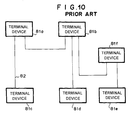
- FIG. 10 is a block diagram showing a network using IEEE1394.
- the respective terminal devices are connected to one another through a feeder-affixed twisted pair line 82 into which a transmission path based on the IEEE1394 standard and a feeder are unified, and each terminal device applies a bias voltage to a twisted pair line.
- the terminal device concerned detects variation of the bias voltage to detect the insertion/removal of the feeder-affixed twisted pair line and transmits a reset signal to initialize an IEEE1394 network.
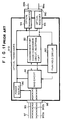
- Fig. 11 is a block diagram showing the construction of a optical transceiver disclosed in Japanese Laid-open patent Application No. Hei-10-41898 which uses an optical fiber as a part of the transmission path.
- the optical transceiver is connected to a terminal device through a feeder-affixed twisted pair line based on the IEEE1394 standard, and an optical fiber can be used for a part of the transmission path of the IEEE1394 network.
- optical transceiver The operation of the optical transceiver will be described hereunder.
- the optical transceiver used through the optical fiber comprises a bias circuit 91, a code conversion circuit 92, a peak hold circuit 93, a optical transmitter 94, a optical receiver 95, a power circuit 96, an electrical connector 98 to which a feeder-affixed twisted pair line 97 based on the IEEE1394 standard is connected, and an optical connector 910 to which an optical fiber 99 is connected.
- the optical transmitter 94 converts an electrical signal from the code conversion circuit 92 to an optical signal, and transmits the optical signal thus converted through the optical connector 910 onto an optical fiber 99b.
- the optical transmitter 94 has a function of converting the optical signal received by the optical connector 910 to an electrical signal, performing waveform shaping and then outputting it to the code conversion circuit 92 and the peak hold circuit 93.
- the feeder-affixed twisted pair line 97 has two twisted pair lines, and signals of two lines exist in the feeder-affixed twisted pair line 97.
- the code conversion circuit 92 has a function of converting the signals of two lines to signals of one line so that the signals of two lines can be transmitted through the optical fiber 99 when an optical transmission is outputted, and a function of converting the optical signals of one line thus received to signals of two lines so that the signals can be transmitted on a twisted pair line.
- the peak hold circuit 93 has a function of detecting the presence or absence of an optical signal on the basis of the electrical signal which is converted from the optical signal by the optical receiver 95, and a function of controlling the bias circuit 91 on the basis of the detection result.
- the bias circuit 91 has a function of applying a bias voltage to each twisted pair line 912a and 912b of the feeder-affixed twisted pair line 97 connected to the electric connector 98, and it is controlled on the basis of the output of the peak hold circuit 93.
- a terminal device when it receives an optical signal, it applies a bias voltage to the twisted pair line 912a and 912b, and when it receives no optical signal, it stops the voltage application, whereby a terminal device can detect insertion/removal of a feeder-affixed twisted pair line 912a and 912b or insertion/removal of an optical fiber 99a and 99b to initialize the IEEE1394 serial bus.
- a communication system based on optical or electrical waves by using space as a medium may be utilized from the viewpoint that rewiring due to movement of terminal devices or arrangement of twisted pair lines (cables) in a wiring process spoils the beauty of the appearance.
- the radio transmission system based on optical technique is called as “optical spatial transmission system", and it is described in "FUNDAMENTALS OF OPTOELECTRONICS" p. 26 issued by Keigaku Publication Co., Ltd., for example.
- Fig. 12 is a block diagram showing an optical spatial transmission device disclosed in Japanese Laid-open Patent Application No. Hei-7-183849. The construction and operation of the optical spatial transmission device will be briefly described with reference to Fig. 12.
- a transmitter 101 includes an encode circuit 102 for converting an input information signal to a base band code, a driver circuit 103 for driving a optical emission unit 104 on the basis of the base band code, and the optical emission unit 104 for converting an electrical signal from the driver circuit 103 to an optical signal and discharging the optical signal to space.
- a receiver 105 includes a optical reception unit 106 for receiving the optical signal from a spatial transmission path and converting the received optical signal to an electrical signal, a clock reproducing circuit 107 for reproducing a clock signal from the received optical signal, and a decode circuit 108 for reproducing a base band code from the reproduced clock signal and the electrical signal from the optical receiving unit 106, and outputting an information signal.
- the optical spatial transmission system is applied to the optical transmission/reception portion of the optical transceiver of Fig. 11.
- the optical spatial transmission device receives the reflection signal and thus cannot detect the interception of the communication path. Therefore, erroneous data are delivered to a terminal device, and thus the terminal device operates abnormally.
- An object of the present invention is to provide a spatial transmission optical transceiver which can transmit/receive an optical signal through space serving as a communication medium between terminal devices in a network in which plural terminal devices are connected to one another through a data transmission line based on IEEE1394.
- a spatial transmission optical transceiver is characterized by detecting interception of a communication path and insertion/removal of a data transmission line connected to a confronting optical transceiver for spatial transmission.
- the spatial transmission optical transceiver of the present invention detects the interception of the communication path.
- the spatial transmission optical transceiver according to the present invention includes optical signal detection means for detecting the presence or absence of an optical signal on a spatial transmission path, and reflection signal detecting means for detecting that a reception signal is a reflection signal on the basis of a transmitted/received signal.
- the spatial transmission optical transceiver according to the present invention is characterized by detecting the interception of the communication path or the insertion/removal of a signal line and notifying the detection result to a terminal device.
- communication path interception/signal line insertion/removal notifying means for detecting the interception of the communication path and the insertion/removal of the data transmission line connected to the confronting spatial transmission optical transceiver are detected, and notifying the detection result to the terminal device.
- the insertion/removal of the data transmission line connected to the confronting spatial transmission optical transceiver and the interception of the communication path can be detected on the basis of the presence or absence of the optical signal. Further, the interception of the communication path can be detected by detecting the reflection signal due to the interception of the communication path in the neighborhood of the spatial transmission optical transceiver. When there is no reception signal, it is judged that the data transmission lime is removed or the communication path is intercepted, and this fact is notified to the terminal device.
- the received optical signal is detected to be a reflection signal to thereby detect the interception of the communication path, and this fact is notified to the terminal device, whereby the terminal device can detect the insertion/removal of the data transmission line and the interception of the communication path, and thus a reset signal serving as a sign to initialize the network.
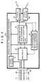
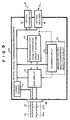
- Fig. 1 is a block diagram showing the construction of a spatial transmission optical transceiver according to a first embodiment of the present invention.
- a optical spatial transmission transceiver 110 includes a power circuit 11, a bias circuit 12, an interception and insertion/removal detection circuit 13, a code conversion circuit 14, a optical transmitter 15, a optical receiver 16 and an electrical connector to which a feeder-affixed twisted pair line 17 serving as a data transmission line based on IEEE1394 standard is connected.
- the feeder-affixed twisted pair line 17 and the optical spatial transmission transceiver 110 are connected to each other through the electrical connector 18. Input/output of signals between the feeder-affixed twisted pair line 17 and the optical spatial transmission transceiver 110 is performed through the code conversion circuit 14.
- the code conversion circuit 14 converts to electrical signals of one line electrical signals of two lines which are input from the feeder-affixed twisted pair line 17 through the bias circuit 12, and outputs the electrical signals thus converted to the optical transmitter 15 and the interception and insertion/removal detection circuit 13. Further, the code conversion circuit 14 also has a function of converting electrical signals of one line from the optical receiver 16 to electrical signals of two lines and then transmitting the electrical signals thus converted through the bias circuit 12 to the feeder-affixed twisted pair line 17.
- the optical transmitter 15 has a function of converting an electrical signal to an optical signal and discharging the optical signal thus converted to space.
- the optical receiver 16 has a function of converting to an electrical signal an optical signal which is transmitted through space serving as a medium and performing waveform shaping. In this case, the space is used as a communication medium, however, an optical fiber may be connected to a connector to achieve optical transmission with little loss.
- the interception and insertion/removal detection circuit 13 has a function of detecting the presence or absence of an optical signal on the basis of a reception signal input from the optical receiver 16 and a transmission signal input from the code conversion circuit 14, and also a function of detecting whether the optical signal received by the optical receiver 16 is a reflection signal of the optical signal transmitted therefrom.
- the power circuit 11 has a function of converting, to a voltage level used in the optical transceiver, a DC voltage which is supplied from the feeder 19 of the feeder-affixed twisted pair line 17 serving as the data transmission line based on the IEEE1394 standard. Further, it also has a function of supplying the DC voltage to another connected equipment on the basis of the IEEE1394 standard.
- the bias circuit 12 has a function of applying a bias voltage to each twisted pair line 111a, 111b of the feeder-affixed twisted pair line 17 connected to the electrical connector 18, and it can control the application of the bias voltage on the basis of the output of the interception and insertion/removal detection circuit 13.
- it is necessary to supply the two twisted pair lines with DC voltage indexing 0, 1, z for specifying the data structure before a start packet for data transmission is transmitted, and this operation is performed by the bias circuit 12.
- Fig. 2 shows an example of the insertion and insertion/removal detection circuit 13.
- the interception and insertion/removal detection circuit 13 comprises an optical signal detection circuit 26, a reflection signal detection circuit 22 and a judgment circuit 25.
- the optical receiver 16 converts the received optical signal to an electrical signal, and inputs the electrical signal thus converted to the optical signal detection circuit 26 and the reflection signal detection circuit 22.
- the optical signal detection circuit 26 comprises a peak hold circuit 21, and it detects the presence or absence of the optical signal on the basis of the input electrical signal and outputs the detection result.
- the reflection signal detection circuit 22 comprises an exclusive OR circuit 23, an averaging circuit 27 for averaging the amplitude of an output signal from the exclusive OR circuit 23, and a signal detection circuit 24, and the reflection signal detection circuit 22 receives, as input signals, an electrical signal (transmission signal) transmitted from a transmission port of the code conversion circuit 15, and an electrical signal (reception signal) to which the optical signal received by the optical receiver 16 is converted.
- the reflection signal detection circuit 22 judges on the basis of the input transmission signal and reception signal whether the reception signal is the reflection signal, and outputs the judgment result.
- the judgment circuit 25 takes the logical product between the detection signal from the optical signal detection circuit 26 and the detection signal from the reflection signal detection circuit 22, and outputs the result to the interception and insertion/removal detection result.
- a communication mode between terminal devices as shown in Fig. 3 is provided as an example. Referring to Fig. 4, it is assumed that neither the interception of the communication path occurs, nor the insertion/removal of the feeder-affixed twisted pair line 17 connected to the confronting optical transceiver occurs during the time period from T0 to T1. At this time, the peak hold circuit 21 of the optical signal detection circuit 26 of the interception and insertion/removal detection circuit 13 detects the signal to output a voltage of H level. Further, the exclusive OR circuit 23 of the reflection signal detection circuit 22 takes the exclusive OR between the input transmission signal and reception signal.
- the optical signal received by the optical spatial transmission transceiver 110a is transmitted from the optical spatial transmission transceiver 110b, and there is no correlation relationship between the transmission signal and the reception signal at the optical spatial transmission transceiver 110a. Accordingly, a random signal which has no correlation with the transmission signal is output from the exclusive OR circuit 23, and the output voltage of the averaging circuit 27 for averaging the amplitude voltage of the output signal from the exclusive OR circuit 23 is above a threshold value of the signal detection circuit 24, so that the signal detection circuit 24 outputs a voltage of H level.
- the judgment circuit 25 takes the logical product between the output of the reflection signal detection circuit 22 and the output of the peak hold circuit 22 of the optical signal detection circuit 26, and outputs an H-level signal.
- the input from the optical receiver 16 to the peak hold circuit 21 of the optical signal detection circuit 26 is set to L-level, and thus the peak hold circuit 21 outputs a voltage of L level.
- the exclusive OR circuit 23 of the reflection signal detection circuit 23 outputs the same signal as the transmission signal, and the output voltage of the averaging circuit 27 is above the threshold value of the signal detection circuit 24, so that the signal detection circuit 24 outputs a voltage of H level.
- the judgment circuit 25 takes the logical product between the output of the reflection signal detection circuit 22 and the output of the peak hold circuit 21 of the optical signal detection circuit 26, and outputs a voltage of L level.
- the bias circuit 12 to which the voltage of L level is input stops the bias voltage application to the twisted pair lines 111a, 111b.
- the interception and insertion/removal detection circuit outputs a voltage of H level again, the bias circuit 12 to which the voltage of H level is input applies a bias voltage to each of the twisted pair lines 111a, 111b.
- the communication path is intercepted in the neighborhood of the optical spatial transmission transceiver 110a and the reflection optical is received by the optical receiver 16.
- the peak hold circuit 21 of the optical signal detection circuit 26 to which the electrical signal is input from the optical receiver 16 outputs the voltage of H level.
- the reception signal (reflection signal) which is input to the exclusive OR circuit 23 of the reflection signal detection circuit 22 is shifted in synchronization with respect to the transmission signal by the delay time, and the exclusive OR circuit 23 outputs the H-level voltage for the delay time between the signal from the optical receiver 16 and the signal from the transmission port.
- the output voltage of the averaging circuit 27 is reduced to be below the threshold value of the signal detection circuit 24, so that the signal detection circuit 24 outputs the L-level voltage.
- the judgment circuit 25 takes the logical product between the output of the reflection signal detection circuit 22 and the output of the peak hold circuit 21 of the optical signal detection circuit 26, and outputs the L-level voltage.
- the bias circuit 12 to which the L-level voltage is input stops the application of the bias voltage to the twisted pair line 111.
- the correlation between the transmission signal and the reception signal is taken to detect the reflection signal.
- the delay time is longer and the correlation between the two signals is weaker.
- the reception signal can be identified as the reflection signal even when the delay time is long.
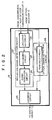
- Fig. 5 is a block diagram showing the construction of the interception and insertion/removal detection circuit 13 of a second embodiment according to the present invention.
- the interception and insertion/removal detection circuit 13 includes delay circuits 41a to 41n, correlation detection circuits 42a to 42n, a reflection signal judgment circuit 43, an optical signal detection circuit 26 and a judgment circuit 25.
- a transmission signal which is input from the code conversion circuit to the interception and insertion/removal detection circuit 13 is delayed by T[s] every time it passes through the delay circuit 41.
- the delay circuit 41 comprises a D-F/F circuit, and T represents the time of one bit of the transmission/reception signal.
- the correlation between the transmission signal passed through each delay circuit 41 and the reception signal input from the optical receiver 16 to the interception and insertion/removal detection 13 is detected by each correlation detection circuit 42.
- the correlation detection circuit 42 outputs an L-level signal (voltage) when the two signals are recognized to have a correlation of predetermined level or more.
- the reflection signal judgment circuit 43 receives the outputs of all the correlation detection circuits 42a to 42n to take the logical product therebetween, and outputs the result.
- the judgment circuit 25 outputs the logical product between the output of the reflection signal judgment circuit 43 and the output of the optical signal detection circuit 26 as a judgment result to the bias circuit 12.
- the reception signal and any one of transmission signals which is passed through the delay circuit 41 and delayed by several bits are necessarily shifted in phase within one bit, and thus the correlation therebetween is high.
- the correlation detection circuit 42 to which the two signals having a high correlation at a predetermined level or more are input outputs the L-level voltage.
- the reflection signal judgment circuit 43 identifies that the reception signal is the reflection signal if at least one of the signals input thereto is L-level, and outputs the L-level voltage.
- the optical signal detection circuit 26 receives the optical signal, and thus outputs the H-level voltage.
- the judgment circuit 25 takes the logical product between the output of the reflection signal judgment circuit 43 and the output of the optical signal detection circuit 26 and outputs the L-level voltage.
- the bias voltage 12 to which the L-level voltage is input stops the bias voltage application to the twisted pair line 111.
- Fig. 6 shows an embodiment of the correlation detection circuit 42.
- the correlation detection circuit 42 has the same construction as the reflection signal detection circuit 22 of the embodiment 1, and it is constructed by the exclusive OR circuit 23, the averaging circuit 22 and the signal detection circuit 24.
- the operation of the correlation detection circuit 42 is the same as the reflection signal detection circuit 22 of the embodiment 1.
- the delay circuit 41 may be implemented by increasing the length of the transmission path so that transmission delay occurs.
- the wavelength of optical emitted from the optical transmitter is varied every optical transceiver and a optical wavelength discriminator is provided at the front side of the optical receiver.
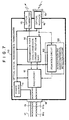
- Fig. 7 is a diagram showing the construction of a optical transceiver according to a third embodiment of the present invention.
- a optical wavelength discriminator 61 is provided at the front stage of the optical receiver 16, and the interception and insertion/removal detection circuit 63 comprises a peak hold circuit 62.
- the wavelength of the optical emitted from the optical transmitter 15 is varied every optical transceiver.
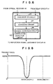
- Fig. 8 shows the transmission characteristic of the optical wavelength discriminator 61.
- an optical signal of wavelength 1 which is emitted from the optical spatial transmission transceiver 110a is discriminated by the optical wavelength discriminator 61 provide at the front stage of the optical receiver 16 of the optical spatial transmission transceiver 110b and then reaches the optical receiver 16.
- the optical signal of wavelength 2 emitted from the optical transceiver 101b is intercepted in the neighborhood of the optical transceiver 101b and becomes reflection optical, the optical signal of wavelength 2 cannot pass through the optical wavelength discriminator 61, and thus cannot reach the optical receiver 16. Therefore, the electrical signal output from the optical receiver 16 is set to L-level, and the interception and insertion/removal detection circuit 63 detects the interception and outputs the L-level voltage to the bias circuit 12.
- the interception and insertion/removal detection circuit 63 can detect the interception state, and control application or non-application of the bias voltage of the transmission/reception circuit corresponding to the twisted pair line 111 of the bias circuit 12.
- the detection of the optical signal is performed by the peak hold circuit.
- the detection of the signal may be performed by using a counter circuit.
- a counter circuit 72 is contained in the interception and insertion/removal detection circuit 71. Further, the counter circuit 72 may be provided in place of the peak hold circuit 21 in the interception and insertion/removal detection circuit 13 as shown in Fig. 2.
- the counter circuit 72 carries out the counter operation at all times. It resets its count value every time an H-level signal is input thereto, and outputs an H-level voltage. When the signal input is kept to L-level during a fixed time, the count value is coincident with a preset judgment value T, and the counter circuit 72 outputs an L-level voltage.
- the insertion/removal of a data transmission line connected to a confronting optical transceiver and the interception of a communication path in the above network can be also detected in the same manner by using the optical transceiver in which the interception and insertion/removal detection circuit 71 is constructed by using the counter circuit 72, and initialization of the IEEE1394 network can be performed.
- the optical transceiver may be installed in the terminal device, and provided with an optical interface.
- an adapter satisfying the IEEE1394 standard may be used not only the above optical transmission path, but also a radio transceiver using radio frequency.
- a transmission route having a DC power supply function and a signal line biasing function can be achieved as same as a route using the IEEE1394 standard.
- adapters which are conformable to USB (Universal Serial Bus), RS-232C and SCSI standards in place of IEEE1394 may be used.
- the spatial transmission optical transceiver thus constructed, the removal of the feeder-affixed twisted pair lines which are connected to a confronting optical transceiver and conformable to the IEEE1394 standard, and the interception of the communication path can be detected. Therefore, even when an optical spatial transmission system using a spatial medium for a part of the transmission path is applied, the initialization of the IEEE1394 network, that is, the address setting of the network, recognition of connected equipment, etc. can be performed. Accordingly, in the IEEE1394 network, an optical communication system using space as a communication medium can be used, and the rewiring problem due to the movement of the terminal devices and the problem of spoiling the beauty of the appearance due to the arrangement of cables can be solved.
- the optical transceiver of the present invention it can be detected whether the reception signal is caused by the reflection optical, and thus the initialization of the IEEE1394 network can be performed irrespective of the interception in the neighborhood of the optical transceiver.
Landscapes
- Physics & Mathematics (AREA)
- Electromagnetism (AREA)
- Engineering & Computer Science (AREA)
- Computer Networks & Wireless Communication (AREA)
- Signal Processing (AREA)
- Optical Communication System (AREA)
Abstract
Description
Claims (10)
- A spatial transmission optical transceiver based on IEEE1394 standard, comprising:a data transmission line for being terminated based on IEEE1394 standard;a code conversion circuit for converting an electrical signal from a terminal device to an optical signal to emit the optical signal to space and converting an optical signal to an electrical signal to output the electrical signal to said data transmission line;an optical receiver for receiving a optical signal transmitted through the space to convert the optical signal;an optical signal detection means for detecting one of the presence and absence of the optical signal received by said spatial transmission optical transceiver;a reflection signal detection means for detecting that the reception signal received by said spatial transmission optical transceiver is a reflection signal;a judgment circuit for detecting interception of a communication path and insertion/removal of the data transmission line connected to a confronting optical transceiver on the basis of the detection result of said optical signal detection means and said reflection signal detection means; andpath interception and signal-line insertion/removal notifying means for notifying the detection result to a terminal device.
- The spatial transmission optical transceiver as claimed in claim 1,
wherein said judgment circuit comprises a circuit for taking the logical product between the detection result of said reflection signal detection means and the detection result of said optical signal detection means to detect the interception of the communication path and the insertion/removal of the data transmission line connected to the confronting optical transceiver. - The spatial transmission optical transceiver as claimed in claim 1,
wherein said reflection signal detection means comprises an exclusive OR circuit for taking the exclusive OR between the electrical signal to which the received optical signal is converted and the transmitted electrical signal, an averaging circuit for averaging the amplitude of the output signal of said exclusive OR circuit, and a detection circuit for detecting the signal on the basis of the output voltage thereof. - The spatial transmission optical transceiver as claimed in claim 1,
wherein said reflection signal detection means comprises plural delay circuits for delaying the transmitted electrical signal, an exclusive OR circuit for taking the exclusive OR between the output signal of each of said delay circuits and the electrical signal to which the received optical signal is converted, an averaging circuit for averaging the amplitude of the output signal of said exclusive OR circuit; and a detection circuit for detecting the signal on the basis of the output voltage thereof. - The spatial transmission optical transceiver as claimed in claim 1, wherein said path interception and signal-line insertion/removal notifying means comprises a bias circuit to the data transmission line, said bias circuit applying a bias voltage when a communication is made, and stopping the bias voltage application to the data transmission line when the interception of the communication path or the removal of the signal line occurs.
- The spatial transmission optical transceiver as claimed in any of claims 1 to 5, further comprising:a power circuit having a function of converting, to a voltage level used in said code conversion circuit and said optical receiver, a DC voltage which is supplied from a feeder of a feeder-affixed twisted pair line based on the IEEE1394 standard.
- The spatial transmission optical transceiver as claimed in any of claims 1 to 6, further comprising:a bias circuit having a function of applying a bias voltage to a data transmission line for being terminated based on IEEE1394 standard according to the result of said optical signal detection means.
- A spatial transmission optical transceiver in which a data transmission line based on IEEE1394 standard is terminated, an electrical signal from a terminal device is converted to an optical signal to emit the optical signal to space, and the optical signal transmitted through the space is received to convert the optical signal thus received to an electrical signal and transmit the electrical signal to the data transmission line, comprising:optical wavelength discriminating means for inhibiting pass of reflection optical therethrough and allowing transmission of signal optical which is emitted from a confronting spatial transmission optical transceiver and has wavelength different from the wavelength of the optical transmitted from a optical transmitter of said spatial transmission optical transceiver concerned;optical signal detection means for detecting the presence or absence of the optical signal received by said spatial transmission optical transceiver; andpath interception and signal-line insertion/removal notifying means for notifying the detection result to a terminal device.
- The spatial transmission optical transceiver as claimed in claim 8, further comprising:a power circuit having a function of converting, to a voltage level used in said code conversion circuit and said optical receiver, a DC voltage which is supplied from a feeder of a feeder-affixed twisted pair line based on the IEEE1394 standard.
- The spatial transmission optical transceiver as claimed in claim 8 or 9, further comprising:a bias circuit having a function of applying a bias voltage to a data transmission line for being terminated based on IEEE1394 standard according to the result of said optical signal detection means.
Applications Claiming Priority (6)
| Application Number | Priority Date | Filing Date | Title |
|---|---|---|---|
| JP26664297 | 1997-09-30 | ||
| JP26664297 | 1997-09-30 | ||
| JP266642/97 | 1997-09-30 | ||
| JP04908298A JP3529263B2 (en) | 1997-09-30 | 1998-03-02 | Optical transmission / reception circuit for space transmission and space transmission device |
| JP4908298 | 1998-03-02 | ||
| JP49082/98 | 1998-03-02 |
Publications (3)
| Publication Number | Publication Date |
|---|---|
| EP0905924A2 true EP0905924A2 (en) | 1999-03-31 |
| EP0905924A3 EP0905924A3 (en) | 2004-03-03 |
| EP0905924B1 EP0905924B1 (en) | 2007-01-31 |
Family
ID=26389435
Family Applications (1)
| Application Number | Title | Priority Date | Filing Date |
|---|---|---|---|
| EP98118322A Expired - Lifetime EP0905924B1 (en) | 1997-09-30 | 1998-09-28 | Spatial transmission light transceiver |
Country Status (4)
| Country | Link |
|---|---|
| US (1) | US6678477B1 (en) |
| EP (1) | EP0905924B1 (en) |
| JP (1) | JP3529263B2 (en) |
| DE (1) | DE69837000T2 (en) |
Cited By (3)
| Publication number | Priority date | Publication date | Assignee | Title |
|---|---|---|---|---|
| WO2001006680A1 (en) * | 1999-07-19 | 2001-01-25 | Thomson Licensing S.A. | Electrical insulation device with optocoupler for bidirectional connecting lines |
| RU2407168C1 (en) * | 2009-07-09 | 2010-12-20 | Федеральное государственное учреждение 16 Центральный научно-исследовательский испытательный институт Министерства обороны Российской Федерации имени маршала войск связи А.И. Белова | Transceiver for fibre-optic communication line |
| RU2679823C1 (en) * | 2018-01-31 | 2019-02-13 | Федеральное государственное казенное военное образовательное учреждение высшего образования "Академия Федеральной службы охраны Российской Федерации" (Академия ФСО России) | Optical transceiver |
Families Citing this family (10)
| Publication number | Priority date | Publication date | Assignee | Title |
|---|---|---|---|---|
| JPH11338587A (en) * | 1998-05-26 | 1999-12-10 | Matsushita Electric Ind Co Ltd | Non-contact information transmission device |
| JP2001308955A (en) * | 2000-04-20 | 2001-11-02 | Sharp Corp | Transmission method |
| JP2002176466A (en) * | 2000-12-08 | 2002-06-21 | Fuji Film Microdevices Co Ltd | Signal processing circuit and signal processing method |
| US6842439B2 (en) * | 2002-06-17 | 2005-01-11 | Harris Corporation | Free space optical terminal with ad hoc network back-up and associated methods |
| JP2004153557A (en) * | 2002-10-30 | 2004-05-27 | Sumitomo Electric Ind Ltd | Optical transceiver module |
| US20050053381A1 (en) * | 2003-08-12 | 2005-03-10 | Lockheed Martin Corporation | Repeater node and serial bus system therefor |
| US7533203B2 (en) * | 2004-05-06 | 2009-05-12 | Texas Instruments Incorporated | Method and system for rapidly starting up an IEEE 1394 network |
| US20110221601A1 (en) * | 2010-03-12 | 2011-09-15 | Jerry Aguren | Detecting Engagement Conditions Of A Fiber Optic Connector |
| JP6915269B2 (en) * | 2016-12-27 | 2021-08-04 | セイコーエプソン株式会社 | robot |
| US10530559B2 (en) * | 2017-11-28 | 2020-01-07 | Marvell World Trade Ltd. | Ethernet transceiver with PHY-level signal-loss detector |
Family Cites Families (27)
| Publication number | Priority date | Publication date | Assignee | Title |
|---|---|---|---|---|
| JPS581361A (en) * | 1981-06-26 | 1983-01-06 | Hitachi Ltd | Data communication method |
| JPH02223249A (en) | 1989-02-23 | 1990-09-05 | Matsushita Electric Works Ltd | Data transmission system |
| JPH02280545A (en) | 1989-04-21 | 1990-11-16 | Matsushita Electric Ind Co Ltd | Optical space transmitter |
| AU7156091A (en) * | 1989-12-14 | 1991-07-18 | Bicc Network Solutions, Inc. | Free space local area network system |
| US5142400A (en) * | 1989-12-26 | 1992-08-25 | Cubic Corporation | Method and apparatus for automatic acquisition and alignment of an optical beam communication link |
| JPH03203420A (en) | 1989-12-28 | 1991-09-05 | Nec Corp | Optical transmission system |
| JPH03239027A (en) | 1990-02-16 | 1991-10-24 | Nippon Telegr & Teleph Corp <Ntt> | Optical input interruption detection system |
| US5229593A (en) * | 1991-10-08 | 1993-07-20 | International Business Machines Corporation | Apparatus and method for safe, free space laser communication |
| JPH05153057A (en) | 1991-11-26 | 1993-06-18 | Matsushita Electric Works Ltd | Optical space transmission system |
| JPH06132898A (en) | 1992-10-21 | 1994-05-13 | Nec Corp | Optical transmission circuit |
| JPH07107037A (en) | 1993-09-30 | 1995-04-21 | Kokusai Electric Co Ltd | Spatial optical communication device and spatial optical communication method thereof |
| WO1995015624A1 (en) * | 1993-12-02 | 1995-06-08 | Radiance Communications, Inc | Infrared local area network |
| JPH07183849A (en) | 1993-12-22 | 1995-07-21 | N T T Data Tsushin Kk | Optical space transmission method and device |
| JPH07212280A (en) | 1994-01-14 | 1995-08-11 | Fujitsu Ltd | Communication device self-diagnosis method |
| US5600471A (en) * | 1994-04-28 | 1997-02-04 | Victor Company Of Japan, Ltd. | Optical wireless data transmission system and optical wireless data transmitting/receiving apparatus |
| JP3137167B2 (en) * | 1994-08-10 | 2001-02-19 | 日本ビクター株式会社 | Transceiver and return light canceling method |
| JP3239027B2 (en) | 1994-09-08 | 2001-12-17 | ソニー株式会社 | Packaging box |
| JPH0897773A (en) * | 1994-09-27 | 1996-04-12 | Fujitsu Ltd | Optical signal transmission device |
| JPH09149325A (en) | 1995-11-21 | 1997-06-06 | Sony Corp | Graphic display data distributed AV system |
| JPH09186574A (en) * | 1995-12-28 | 1997-07-15 | Nec Corp | Terminal equipment with detection function |
| JP2836592B2 (en) | 1996-07-19 | 1998-12-14 | 日本電気株式会社 | Optical transceiver and network using the optical transceiver |
| JP3716508B2 (en) | 1996-08-26 | 2005-11-16 | ソニー株式会社 | Bi-directional optical data communication apparatus and bi-directional optical data communication method |
| JPH10105437A (en) | 1996-09-30 | 1998-04-24 | Nec Corp | System for monitoring remote place host machine fault situation |
| JP3442593B2 (en) | 1996-11-20 | 2003-09-02 | 株式会社東芝 | Network connection device and network connection method |
| US6133933A (en) | 1997-01-13 | 2000-10-17 | Xerox Corporation | Color Xerographic printing system with multicolor printbar |
| JPH10224353A (en) * | 1997-01-31 | 1998-08-21 | Toshiba Corp | Network system and bus arbitration method thereof |
| JP3203420B2 (en) | 1998-05-29 | 2001-08-27 | 兼房株式会社 | Circular saw with hard tip |
-
1998
- 1998-03-02 JP JP04908298A patent/JP3529263B2/en not_active Expired - Fee Related
- 1998-09-22 US US09/158,583 patent/US6678477B1/en not_active Expired - Fee Related
- 1998-09-28 EP EP98118322A patent/EP0905924B1/en not_active Expired - Lifetime
- 1998-09-28 DE DE69837000T patent/DE69837000T2/en not_active Expired - Lifetime
Cited By (4)
| Publication number | Priority date | Publication date | Assignee | Title |
|---|---|---|---|---|
| WO2001006680A1 (en) * | 1999-07-19 | 2001-01-25 | Thomson Licensing S.A. | Electrical insulation device with optocoupler for bidirectional connecting lines |
| US6775438B1 (en) | 1999-07-19 | 2004-08-10 | Thomson Licensing S.A. | Electrical insulation device with optocoupler for bidirectional connecting lines |
| RU2407168C1 (en) * | 2009-07-09 | 2010-12-20 | Федеральное государственное учреждение 16 Центральный научно-исследовательский испытательный институт Министерства обороны Российской Федерации имени маршала войск связи А.И. Белова | Transceiver for fibre-optic communication line |
| RU2679823C1 (en) * | 2018-01-31 | 2019-02-13 | Федеральное государственное казенное военное образовательное учреждение высшего образования "Академия Федеральной службы охраны Российской Федерации" (Академия ФСО России) | Optical transceiver |
Also Published As
| Publication number | Publication date |
|---|---|
| DE69837000T2 (en) | 2007-10-18 |
| US6678477B1 (en) | 2004-01-13 |
| DE69837000D1 (en) | 2007-03-22 |
| EP0905924A3 (en) | 2004-03-03 |
| JPH11168436A (en) | 1999-06-22 |
| JP3529263B2 (en) | 2004-05-24 |
| EP0905924B1 (en) | 2007-01-31 |
Similar Documents
| Publication | Publication Date | Title |
|---|---|---|
| EP0905924B1 (en) | Spatial transmission light transceiver | |
| US4850042A (en) | Dual media local area network interfacing | |
| EP0113231B1 (en) | Data transmission system with modems coupled to a common communication medium | |
| US7036031B2 (en) | Electronic device and its power control method | |
| EP0622711B1 (en) | Digital communication network data transmission method and apparatus | |
| AU1726988A (en) | Apparatus and method for providing a wireless link between two local area network systems | |
| JP2836592B2 (en) | Optical transceiver and network using the optical transceiver | |
| US11580053B2 (en) | Serial bus signal conditioner for detecting initiation of or return to high-speed signaling | |
| EP0476444A1 (en) | Optical transceiver | |
| CN112988648A (en) | Communication method, device and communication circuit | |
| RU2586580C2 (en) | Conflict detection in eia-485 buses | |
| EP0112126A2 (en) | Communication network and method for its use | |
| US4584575A (en) | Method and device for the asynchronous series communication on the multipoint type of a plurality of logic transceivers | |
| EP0174182B1 (en) | Information transmission system in a local area network suitable for collision detection | |
| US4602252A (en) | Method and device for data communication | |
| EP1196854B1 (en) | Method and apparatus for generating a control signal bitstream | |
| US6993082B2 (en) | Station and method for operating a CAN communication line | |
| US4683471A (en) | Data bus pilot tone | |
| JP2001211124A (en) | Optical transmitting and receiving circuit for spatial transmission, and spatial transmission device | |
| GB2226202A (en) | Optical transmission device | |
| FI112548B (en) | Arrangements for data transfer | |
| US5010480A (en) | Communication interface for interfacing a data bus of a computer to a high speed bipolar communication system | |
| KR100367428B1 (en) | LAN Interface Unit for Internet Interface Units_ | |
| EP0146045B1 (en) | Digital data transceiver for power line communications system | |
| KR20010057825A (en) | apparatus of packet transmission in ethernet interface system |
Legal Events
| Date | Code | Title | Description |
|---|---|---|---|
| PUAI | Public reference made under article 153(3) epc to a published international application that has entered the european phase |
Free format text: ORIGINAL CODE: 0009012 |
|
| AK | Designated contracting states |
Kind code of ref document: A2 Designated state(s): AT BE CH CY DE DK ES FI FR GB GR IE IT LI LU MC NL PT SE |
|
| AX | Request for extension of the european patent |
Free format text: AL;LT;LV;MK;RO;SI |
|
| PUAL | Search report despatched |
Free format text: ORIGINAL CODE: 0009013 |
|
| AK | Designated contracting states |
Kind code of ref document: A3 Designated state(s): AT BE CH CY DE DK ES FI FR GB GR IE IT LI LU MC NL PT SE |
|
| AX | Request for extension of the european patent |
Extension state: AL LT LV MK RO SI |
|
| 17P | Request for examination filed |
Effective date: 20040121 |
|
| 17Q | First examination report despatched |
Effective date: 20040506 |
|
| AKX | Designation fees paid |
Designated state(s): DE FR GB |
|
| RTI1 | Title (correction) |
Free format text: OPTICAL FREE SPACE TRANSCEIVER |
|
| GRAP | Despatch of communication of intention to grant a patent |
Free format text: ORIGINAL CODE: EPIDOSNIGR1 |
|
| GRAS | Grant fee paid |
Free format text: ORIGINAL CODE: EPIDOSNIGR3 |
|
| GRAA | (expected) grant |
Free format text: ORIGINAL CODE: 0009210 |
|
| RIN1 | Information on inventor provided before grant (corrected) |
Inventor name: YAMAZAKI, SHUNTARO Inventor name: MATSUDA, JUNICHI |
|
| RTI1 | Title (correction) |
Free format text: SPATIAL TRANSMISSION LIGHT TRANSCEIVER |
|
| AK | Designated contracting states |
Kind code of ref document: B1 Designated state(s): DE FR GB |
|
| REG | Reference to a national code |
Ref country code: GB Ref legal event code: FG4D |
|
| REF | Corresponds to: |
Ref document number: 69837000 Country of ref document: DE Date of ref document: 20070322 Kind code of ref document: P |
|
| ET | Fr: translation filed | ||
| PLBE | No opposition filed within time limit |
Free format text: ORIGINAL CODE: 0009261 |
|
| STAA | Information on the status of an ep patent application or granted ep patent |
Free format text: STATUS: NO OPPOSITION FILED WITHIN TIME LIMIT |
|
| 26N | No opposition filed |
Effective date: 20071101 |
|
| PGFP | Annual fee paid to national office [announced via postgrant information from national office to epo] |
Ref country code: GB Payment date: 20090923 Year of fee payment: 12 |
|
| PGFP | Annual fee paid to national office [announced via postgrant information from national office to epo] |
Ref country code: DE Payment date: 20090923 Year of fee payment: 12 |
|
| PGFP | Annual fee paid to national office [announced via postgrant information from national office to epo] |
Ref country code: FR Payment date: 20091012 Year of fee payment: 12 |
|
| GBPC | Gb: european patent ceased through non-payment of renewal fee |
Effective date: 20100928 |
|
| REG | Reference to a national code |
Ref country code: FR Ref legal event code: ST Effective date: 20110531 |
|
| REG | Reference to a national code |
Ref country code: DE Ref legal event code: R119 Ref document number: 69837000 Country of ref document: DE Effective date: 20110401 |
|
| PG25 | Lapsed in a contracting state [announced via postgrant information from national office to epo] |
Ref country code: DE Free format text: LAPSE BECAUSE OF NON-PAYMENT OF DUE FEES Effective date: 20110401 Ref country code: FR Free format text: LAPSE BECAUSE OF NON-PAYMENT OF DUE FEES Effective date: 20100930 |
|
| PG25 | Lapsed in a contracting state [announced via postgrant information from national office to epo] |
Ref country code: GB Free format text: LAPSE BECAUSE OF NON-PAYMENT OF DUE FEES Effective date: 20100928 |