EP0905947A2 - Procédé et dispositif de modulation/démodulation - Google Patents
Procédé et dispositif de modulation/démodulation Download PDFInfo
- Publication number
- EP0905947A2 EP0905947A2 EP98113707A EP98113707A EP0905947A2 EP 0905947 A2 EP0905947 A2 EP 0905947A2 EP 98113707 A EP98113707 A EP 98113707A EP 98113707 A EP98113707 A EP 98113707A EP 0905947 A2 EP0905947 A2 EP 0905947A2
- Authority
- EP
- European Patent Office
- Prior art keywords
- bit
- modulation
- signal
- output
- bits
- Prior art date
- Legal status (The legal status is an assumption and is not a legal conclusion. Google has not performed a legal analysis and makes no representation as to the accuracy of the status listed.)
- Ceased
Links
Images


Classifications
-
- H—ELECTRICITY
- H03—ELECTRONIC CIRCUITRY
- H03M—CODING; DECODING; CODE CONVERSION IN GENERAL
- H03M1/00—Analogue/digital conversion; Digital/analogue conversion
-
- H—ELECTRICITY
- H04—ELECTRIC COMMUNICATION TECHNIQUE
- H04L—TRANSMISSION OF DIGITAL INFORMATION, e.g. TELEGRAPHIC COMMUNICATION
- H04L25/00—Baseband systems
- H04L25/38—Synchronous or start-stop systems, e.g. for Baudot code
- H04L25/40—Transmitting circuits; Receiving circuits
- H04L25/49—Transmitting circuits; Receiving circuits using code conversion at the transmitter; using predistortion; using insertion of idle bits for obtaining a desired frequency spectrum; using three or more amplitude levels ; Baseband coding techniques specific to data transmission systems
- H04L25/4906—Transmitting circuits; Receiving circuits using code conversion at the transmitter; using predistortion; using insertion of idle bits for obtaining a desired frequency spectrum; using three or more amplitude levels ; Baseband coding techniques specific to data transmission systems using binary codes
- H04L25/4908—Transmitting circuits; Receiving circuits using code conversion at the transmitter; using predistortion; using insertion of idle bits for obtaining a desired frequency spectrum; using three or more amplitude levels ; Baseband coding techniques specific to data transmission systems using binary codes using mBnB codes
Definitions
- the present invention relates to a transmitter/receiver capable of infrared-communicating with a personal computer, a portable information terminal and other home use instruments, which has an infrared communication function, and more specifically to a modulation/demodulation method and apparatus for transferring a large amount of data by use of infrared.
- a prior art modulation/demodulation system used in an infrared communication of a personal computer is one called a "4 pulse position modulation” (called a “4PPM” hereinafter).
- the 4PPM is that an input signal of two bits is modulated to a modulation signal in which one word consists of four bits.
- the modulation signal has a pulse on only one bit within each one word, and the position of the pulse in the word is different from one pattern of an input signal to another.
- a first bit is called “a”
- a second bit is called “b”.
- a third bit is called “c” and a fourth bit is called “d”.
- a first timing chart illustrating the input signal and the modulation signal in the 4PPM system.
- the modulation signal is in synchronism with the rising of a modulation clock, and the modulation signal is constituted of four bits (namely, one word) with four modulation clocks.
- the input signal is in synchronism with the rising of an input clock, and the input signal is constituted of two bits (namely, one word) with two input clocks.
- the frequency of the input clock is a half the frequency of the modulation clock. For example, if the input clock is 4MHz, the modulation clock becomes 8MHz. In this case, the transfer rate is 4Mbps (Mega bit per second).
- a first bit, a second bit, a third bit and a fourth bit in one word of the modulation signal are called "a", "b", "c” and "d", respectively.
- the first word corresponds to the input signal "00” and the modulation signal has the pulse positioned on the first bit "a”.
- the second word corresponds to the input signal "01” and the modulation signal has the pulse positioned on the second bit "b”.
- the third word corresponds to the input signal "10” and the modulation signal has the pulse positioned on the third bit "b”.
- the fourth word corresponds to the input signal "11” and the modulation signal has the pulse positioned on the fourth bit "d”.
- Fig. 11 illustrates the waveform of the modulation signal in a situation in which the fourth word shown in Fig. 10 follows the first word shown in Fig. 10.
- the modulation signal has the pulse positioned at the bit "a” in the first word and the pulse positioned at the bit "d” in the fourth word. In this case, six bits having no pulse continues from the bit "b" of the first word to the bit "c" of the fourth word.
- the bit width of continuing bits having no pulse is 6 bits as shown in Fig. 11.
- Fig. 12 illustrates the waveform of the modulation signal in a situation in which the first word shown in Fig. 10 follows the fourth word shown in Fig. 10.
- the modulation signal has the pulse positioned at the bit "d" in the fourth word and the pulse positioned at the bit "a" in the first word. In this case, only two bits having the pulse continues at maximum.
- the bit width of continuing bits having the pulse is 2 bits as shown in Fig. 11.
- the pulse width of the modulation signal is influenced with a response characteristics of an infrared light emitting diode.
- the pulse width of the modulation signal emitted from the infrared light emitting diode and therefore influenced by the response characteristics of the infrared light emitting diode becomes wide or narrow in comparison with an inherent pulse width of the modulation signal.
- the modulation signal influenced by the response characteristics of the infrared light emitting diode is not synchronized with the modulation clock, with the result that a normal communication cannot be obtained.
- the continuing bits of the pulse are two bits at maximum, and the continuing bits of no pulse are six bits at maximum. Therefore, they are relatively small.
- the frequency of the modulation clock increases, the inherent pulse width of the modulation signal becomes narrow, with the result that the response of the infrared light emitting diode cannot follow the change of the modulation signal, and therefore, a normal communication cannot be obtained. Because of these reasons, the prior art infrared communication adopts the modulation system of the 4PPM, the modulation clock frequency of 8MHz, and the transfer rate of 4Mbps.
- FIG. 13 there is shown a circuit diagram illustrating one example of a modulation circuit at a transmitter side in the 4PPM system.
- Reference Numeral 250 designates a two-bit serial-to-parallel conversion circuit
- Reference Numeral 251 denotes a decoder.
- Reference Numeral 252 indicates a four-bit parallel-to-serial conversion circuit.
- Reference Numeral 10-3 shows an input signal supplied to a data input of the two-bit serial-to-parallel conversion circuit 250
- Reference Numeral 11-3 designates an input clock supplied to a clock input of the two-bit serial-to-parallel conversion circuit 250.
- Reference Numeral 12-3 denotes a modulation clock supplied to a clock input of the four-bit parallel-to-serial conversion circuit 252, and Reference Numeral 13-3 indicates a modulation signal outputted from a data output of the four-bit parallel-to-serial conversion circuit 252.
- the above mentioned decoder 251 comprises inverters 351 and 352 and AND gates 451, 452, 453 and 454, which are connected as shown.
- An input of the inverter 351 is connected to a first output of the two-bit serial-to-parallel conversion circuit 250, and an input of the inverter 352 is connected to a second output of the two-bit serial-to-parallel conversion circuit 250.
- the AND gate 451 has inputs connected to the first output and the second output of the two-bit serial-to-parallel conversion circuit 250, respectively.
- the AND gate 452 has inputs connected to an output of the inverter 351 and the second output of the two-bit serial-to-parallel conversion circuit 250, respectively.
- the AND gate 453 has inputs connected to the first output of the two-bit serial-to-parallel conversion circuit 250 and an output of the inverter 352, respectively.
- the AND gate 454 has inputs connected to the output of the inverter 351 and the output of the inverter 352, respectively.
- the four-bit parallel-to-serial conversion circuit 252 has first, second, third and fourth data inputs connected to an output of the AND gates 451, 452, 453 and 454, respectively.
- the two-bit serial-to-parallel conversion circuit 250 captures the two-bit serial data "00" as the input signal 10-3 in synchronism with the input clock 11-3, the two-bit serial-to-parallel conversion circuit 250 outputs "0" from the first output and "0" from the second output.
- the AND gate 451 outputs "0"
- the AND gate 452 outputs "0”
- the AND gate 453 outputs "0”
- the AND gate 454 outputs "1".
- the four-bit parallel-to-serial conversion circuit 252 captures the outputs of the AND gates 451, 452, 453 and 454 at their first, second, third and fourth data inputs, respectively, in parallel.
- the four-bit parallel-to-serial conversion circuit 252 serially outputs the fourth data input, the third data input, the second data input and the first data input in the named order as the modulation signal 13-3.
- the four-bit serial data "1000" is outputted as the modulation signal 13-3. This operation shows the modulation of the first word shown in Fig. 10.
- FIG. 14 there is shown a circuit diagram illustrating one example of a demodulation circuit at a receiver side in the 4PPM system.
- Reference Numeral 253 designates a four-bit serial-to-parallel conversion circuit
- Reference Numeral 254 denotes a encoder.
- Reference Numeral 255 indicates a two-bit parallel-to-serial conversion circuit.
- Reference Numeral 13-4 shows a modulation signal supplied to a data input of the four-bit serial-to-parallel conversion circuit 253, and
- Reference Numeral 12-4 designates a modulation clock supplied to a clock input of the four-bit serial-to-parallel conversion circuit 253.
- Reference Numeral 11-4 denotes an input clock supplied to a clock input of the two-bit parallel-to-serial conversion circuit 255, and Reference Numeral 10-4 indicates an output signal outputted from a data output of the two-bit parallel-to-serial conversion circuit 255.
- the encoder 252 includes two OR gates 551 and 552 connected as shown.
- the OR gate 551 has two inputs connected to a first output and a third output of the four-bit serial-to-parallel conversion circuit 253, respectively.
- the OR gate 552 has two inputs connected to the first output and a second output of the four-bit serial-to-parallel conversion circuit 253, respectively.
- An output of the OR gates 551 and 552 are connected to a first data input and a second data input of the two-bit parallel-to-serial conversion circuit 255, respectively.
- the four-bit serial-to-parallel conversion circuit 253 captures the four-bit serial data "1000" as the modulation signal 13-4 in synchronism with the modulation clock 12-4, the four-bit serial-to-parallel conversion circuit 253 outputs "0", "0", "0” and "1" from the first output, the second output, the third output and the fourth output, respectively.
- the OR gate 551 outputs "0" and the OR gate 552 outputs "0".
- the two-bit parallel-to-serial conversion circuit 255 receives the output of the OR gate 551 at its first data input and the output of the OR gate 552 at its second data input, and serially outputs the second data input and the first data input in the named order in synchronism with the input clock 11-4. In other words, the two-bit serial data "00" is outputted as the output signal 10-4. This operation shows the demodulation of the first word shown in Fig. 10.
- the data transfer rate is determined by the frequency of the input clock.
- the prior art 4PPM system has the input clock frequency of 4MHz, the modulation clock frequency of 8MHz and the data transfer rate of 4Mbps.
- the frequency of the input clock is a half the frequency of the modulation clock. In the prior art 4PPM system, therefore, since data is transmitted after the two-bit input signal is modulated to the four-bit modulation signal, the data transfer rate is low.
- the infrared communication is performed in the 4PPM system, if it is attempted to increase the frequency of the modulation clock in order to elevate the data transfer rate, the response characteristics of the infrared light emitting diode becomes unable to follow the change of the modulation signal. Therefore, it is impossible to increase the frequency of the modulation clock.
- Another object of the present invention is to provide modulation/demodulation method and apparatus having an increased data transfer rate.
- a modulation/demodulation method so configured that at a transmitter side, data is transmitted after an input signal is converted into a modulation signal train composed of serially arranged words each constituted of bits of a predetermined number larger than the bit number of the input signal, and the position of a pulse existing in the word is different from one pattern of the input signal to another, wherein at the transmitter side, the input signal is divided into signal strings each consisting of "n" bits, where "n” is a positive integer larger than "1", and each signal string consisting of "n” bits is converted into a modulation signal string of one word consisting of "n+1” bits, and then, the modulation signal string is serially transmitted bit by bit, and wherein at the receiver side, the signal serially received bit by bit is divided into received signal strings each consisting of "n+1” bits, and each of the received signal strings is demodulated into a demodulated signal string consisting of "n” bits, so that the demodulated
- n is 3 and therefore "n+1” is 4, and the modulation signal string includes eight different patterns of "1000”, “0100”, “0010”, “0001”, “1001”, “0110”, “1010” and "0101".
- a modulation/demodulation apparatus so configured that at a transmitter side, data is transmitted after an input signal is converted into a modulation signal train composed of serially arranged words each constituted of bits of a predetermined number larger than the bit number of the input signal, and the position of a pulse existing in the word is different from one pattern of the input signal to another, wherein the transmitter side includes a first converting means for converting the input signal into signal strings each consisting of "n" bits, where "n” is a positive integer larger than "1", a modulating means for modulating each signal string consisting of "n” bits into a modulation signal string of one word consisting of "n+1” bits, and a first output means for serially outputting the modulation signal string bit by bit.
- a receiver side includes a second converting means for converting the signal serially outputted bit by bit from the first output means of the transmitter side, into received signal strings each consisting of "n+1" bits, a demodulating means for demodulating each received signal string into a demodulated signal string consisting of "n” bits, and a second output means for serially outputting bit by bit the demodulated signal string consisting of "n” bits.
- the modulation means converts a binary signal string of the "n” bits having a 2 n different combinations, into the modulation signal string of one word consisting of the "n+1" bits having 2 n different combination patterns corresponding to the 2 N different combinations in a one-to-one relation.
- the signal value of "1” continues only two signals at maximum, and the signal value of "0" continues only six signals at maximum.
- n is 3 and therefore "n+1” is 4, and the modulation signal string includes eight different patterns of "1000”, “0100”, “0010”, “0001”, “1001”, “0110”, “1010” and "0101".
- the data transfer rate can be elevated to one and half times.
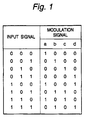
- FIG. 1 there is shown a diagram illustrating a correspondence between the input signal and the modulation signal in one embodiment of the modulation/demodulation system in accordance with the present invention.
- a first bit is called “a”
- a second bit is called “b”.
- a third bit is called “c” and a fourth bit is called “d”.
- the pulse exists on only the first bit "a” in the modulation signal.
- the pulse exists on only the second bit "b” in the modulation signal.
- the pulse exists on only the third bit "c” or the fourth bit "d” in the modulation signal, respectively.
- the pulse exists on the first bit “a” and the fourth bit “d” in the modulation signal.
- the pulse exists on the second bit “b” and the third bit “c” in the modulation signal.
- the pulse exists on the first bit “a” and the third bit “c” in the modulation signal.
- the pulse exists on the second bit "b” and the fourth bit “d” in the modulation signal.
- a first timing chart illustrating the input signal and the modulation signal in the one embodiment of the modulation/demodulation system in accordance with the present invention.
- the modulation signal is in synchronism with the rising of a modulation clock, and the modulation signal of one word consisting of four bits is outputted with four modulation clocks.
- the input signal is in synchronism with the rising of an input clock, and the input signal of one word consisting of three bits is supplied with three input clocks.
- the frequency of the input clock is 3/4 of the frequency of the modulation clock.
- the modulation clock frequency becomes 8MHz.
- the data transfer rate is 6Mbps.
- the construction of the modulation signal of one word is the same as that shown in Fig. 1 and given the same Reference Signs.
- the input signal is "000”, and the pulse exists on only the first bit "a” in the modulation signal.
- the input signal is "001”, the pulse exists on only the second bit "b” in the modulation signal.
- the input signal is "010”, the pulse exists on only the third bit “c” in the modulation signal, respectively.
- the input signal is "011", the pulse exists on only the fourth bit "d” in the modulation signal.
- the input signal is "100”, the pulse exists on the first bit “a” and the fourth bit “d” in the modulation signal.
- the input signal is "101”, the pulse exists on the second bit “b” and the third bit “c” in the modulation signal.
- the input signal is "110”, the pulse exists on the first bit “a” and the third bit “c” in the modulation signal.
- the input signal is "111”, the pulse exists on the second bit "b” and the fourth bit "d” in the modulation signal.
- Fig. 3 illustrates the waveform of the modulation signal in a situation in which the fourth word shown in Fig. 2 follows the first word shown in Fig. 2.
- the modulation signal has the pulse positioned at the bit "a” in the first word and the pulse positioned at the bit "d” in the fourth word. In this case, six bits having no pulse continues from the bit "b" of the first word to the bit "c" of the fourth word.
- the bit width of continuing bits having no pulse is 6 bits as shown in Fig. 3. This is the same as the 4PPM system.
- FIG. 4 there is shown a third timing chart illustrating the input signal and the modulation signal in the one embodiment of the modulation/demodulation system in accordance with the present invention.
- Fig. 4 illustrates the waveform of the modulation signal in a situation in which the fourth word, the fifth word, the seventh word and the sixth word shown in Fig. 2 continues in the named order.
- the pulse continues from the bit “d” in the fourth word to the bit "a” in the fifth word.
- the pulse continues from the bit "d” in the fifth word to the bit "a” in the seventh word.
- the pulse continues from the bit "b” to the bit "c” in the same sixth word.
- the pulse continues over the two continuous bits, but only two bits having the pulse continues at maximum. This is also the same as the 4PPM system.
- FIG. 5 there is shown a circuit diagram illustrating one example of a modulation circuit at a transmitter side in the one embodiment of the modulation/demodulation system in accordance with the present invention.
- Reference Numeral 200 designates a three-bit serial-to-parallel conversion circuit
- Reference Numeral 201 denotes a decoder
- Reference Numeral 202 indicates a four-bit parallel-to-serial conversion circuit
- Reference Numeral 10-1 shows an input signal supplied to a data input D of the three-bit serial-to-parallel conversion circuit 200
- Reference Numeral 11-1 designates an input clock supplied to a clock input C of the three-bit serial-to-parallel conversion circuit 200.
- Reference Numeral 12-1 denotes a modulation clock supplied to a clock input C of the four-bit parallel-to-serial conversion circuit 202
- Reference Numeral 13-1 indicates a modulation signal outputted from a data output Q of the four-bit parallel-to-serial conversion circuit 202.
- First, second and third inputs ID0, ID1 and ID2 of the decoder 201 are connected to first, second and third data outputs Q0, Q1 and Q2 of the three-bit serial-to-parallel conversion circuit 200, respectively.
- First, second, third and fourth outputs OD0, OD1, OD2 and OD3 of the decoder 201 are connected to first, second, third and fourth data inputs D0, D1, D2 and D3 of the four-bit parallel-to-serial conversion circuit 202.
- Fig. 6 is a circuit diagram illustrating one example of the decoder 201 included in the modulation circuit shown in Fig. 5.
- the decoder 201 includes the first input ID0, the second input ID1, the third input ID2, the first output OD0, the second output OD1, the third output OD2, the fourth OD3, inverters 300, 301 and 302, AND gates 400, 401, 402, 403, 404, 405, 406 and 407, and OR gates 500, 501, 502 and 503, which are connected as shown.
- An input of the inverter 300 is connected to the first input ID0, and an input of the inverter 301 is connected to the second input ID1.
- An input of the inverter 302 is connected to the third input ID2.
- Inputs of the AND gate 400 are connected to an output of the inverter 300, an output of the inverter 301 and the third input ID2, respectively.
- Inputs of the AND gate 401 are connected to the first input ID0 and the second input ID1, respectively.
- Inputs of the AND gate 402 are connected to the first input ID0, the output of the inverter 301 and the third input ID2, respectively.
- Inputs of the AND gate 403 are connected to the output of the inverter 300 and the second input ID1, respectively.
- Inputs of the AND gate 404 are connected to the first input ID0 and the output of the inverter 301, respectively.
- Inputs of the AND gate 405 are connected to the first input ID0 and the third input ID2, respectively.
- Inputs of the AND gate 406 are connected to the output of the inverter 300 and the third input ID2, respectively.
- Inputs of the AND gate 407 are connected to the output of the inverter 300 and the output of the inverter 301, respectively.
- Inputs of the OR gate 500 are connected to an output of the AND gate 400 and an output of the AND gate 401, respectively.
- Inputs of the OR gate 501 are connected to an output of the AND gate 402 and an output of the AND gate 403, respectively.
- Inputs of the OR gate 502 are connected to an output of the AND gate 404 and an output of the AND gate 405, respectively.
- Inputs of the OR gate 503 are connected to an output of the AND gate 406 and an output of the AND gate 407, respectively.
- An output of the AND gate 500 is connected to the first output OD0, and an output of the AND gate 501 is connected to the second output OD1.
- An output of the AND gate 502 is connected to the third output OD2, and an output of the AND gate 503 is connected to the fourth OD3.
- the two-bit serial-to-parallel conversion circuit 200 When the three-bit serial-to-parallel conversion circuit 200 captures the three-bit serial data "000" as the input signal 10-1 in synchronism with the input clock 11-1, the two-bit serial-to-parallel conversion circuit 200 outputs "0" from the first output Q0, and "0" from the second output Q1 and “0” from the third output Q2.
- the decoder 201 receiving the outputs of the three-bit serial-to-parallel conversion circuit 200, the first output OD0 outputs "0", the second output OD1 outputs "0”, the third output OD2 outputs "0”, and the fourth output OD3 outputs "1".
- the four-bit parallel-to-serial conversion circuit 222 captures the outputs OD0, OD1, OD2 and OD3 of the decoder 201 at the data inputs D0, D1, D2 and D3 in parallel.
- the four-bit parallel-to-serial conversion circuit 202 serially outputs the fourth data input, the third data input, the second data input and the first data input in the named order as the modulation signal 13-1. Namely, the four-bit serial data "1000" is outputted as the modulation signal 13-1. This operation shows the modulation of the first word shown in Fig. 2.
- the three-bit serial-to-parallel conversion circuit 200 captures the three-bit serial data "001" as the input signal 10-1, the first output Q0 outputs “1”, the second output Q1 outputs “0”, and the third output Q2 outputs "0".
- the first output OD0 of the decoder 201 outputs "0", the second output OD1 outputs “0”, the third output OD2 outputs "1”, and the fourth output OD3 outputs "0".
- the four-bit serial data "0100" is outputted as the modulation signal 13-1. This operation shows the modulation of the second word shown in Fig. 2.
- the three-bit serial-to-parallel conversion circuit 200 captures the three-bit serial data "001" as the input signal 10-1, the first output Q0 outputs “0”, the second output Q1 outputs “1”, and the third output Q2 outputs "0".
- the first output OD0 of the decoder 201 outputs "0", the second output OD1 outputs “1”, the third output OD2 outputs "0”, and the fourth output OD3 outputs "0".
- the four-bit serial data "0010" is outputted as the modulation signal 13-1. This operation shows the modulation of the third word shown in Fig. 2.
- the three-bit serial-to-parallel conversion circuit 200 captures the three-bit serial data "011" as the input signal 10-1, the first output Q0 outputs “1”, the second output Q1 outputs “1”, and the third output Q2 outputs "0".
- the first output OD0 of the decoder 201 outputs "1", the second output OD1 outputs "0”, the third output OD2 outputs "0”, and the fourth output OD3 outputs "0".
- the four-bit serial data "0001" is outputted as the modulation signal 13-1. This operation shows the modulation of the fourth word shown in Fig. 2.
- the three-bit serial-to-parallel conversion circuit 200 captures the three-bit serial data "100" as the input signal 10-1, the first output Q0 outputs “0”, the second output Q1 outputs “0”, and the third output Q2 outputs "1".
- the first output OD0 of the decoder 201 outputs "1", the second output OD1 outputs "0”, the third output OD2 outputs "0”, and the fourth output OD3 outputs "1".
- the four-bit serial data "1001" is outputted as the modulation signal 13-1. This operation shows the modulation of the fifth word shown in Fig. 2.
- the three-bit serial-to-parallel conversion circuit 200 captures the three-bit serial data "101" as the input signal 10-1, the first output Q0 outputs “1", the second output Q1 outputs “0”, and the third output Q2 outputs "1".
- the first output OD0 of the decoder 201 outputs "0", the second output OD1 outputs “1”, the third output OD2 outputs "1”, and the fourth output OD3 outputs "0".
- the four-bit serial data "0110" is outputted as the modulation signal 13-1. This operation shows the modulation of the sixth word shown in Fig. 2.
- the three-bit serial-to-parallel conversion circuit 200 captures the three-bit serial data "110" as the input signal 10-1, the first output Q0 outputs “0”, the second output Q1 outputs “1”, and the third output Q2 outputs "1".
- the first output OD0 of the decoder 201 outputs "0", the second output OD1 outputs “1”, the third output OD2 outputs "0”, and the fourth output OD3 outputs "1".
- the four-bit serial data "1010" is outputted as the modulation signal 13-1. This operation shows the modulation of the seventh word shown in Fig. 2.
- the three-bit serial-to-parallel conversion circuit 200 captures the three-bit serial data "111" as the input signal 10-1, the first output Q0 outputs “1", the second output Q1 outputs “1”, and the third output Q2 outputs "1".
- the first output OD0 of the decoder 201 outputs "1", the second output OD1 outputs "0”, the third output OD2 outputs "1”, and the fourth output OD3 outputs "0".
- the four-bit serial data "0101" is outputted as the modulation signal 13-1. This operation shows the modulation of the eighth word shown in Fig. 2.
- FIG. 7 there is shown a circuit diagram illustrating one example of a demodulation circuit at a receiver side in the one embodiment of the modulation/demodulation system in accordance with the present invention.
- Reference Numeral 203 designates a four-bit serial-to-parallel conversion circuit
- Reference Numeral 204 denotes a encoder
- Reference Numeral 205 indicates a three-bit parallel-to-serial conversion circuit
- Reference Numeral 13-2 shows a modulation signal supplied to a data input D of the four-bit serial-to-parallel conversion circuit 203
- Reference Numeral 12-2 designates a modulation clock supplied to a clock input C of the four-bit serial-to-parallel conversion circuit 203.
- Reference Numeral 11-2 denotes an input clock supplied to a clock input C of the three-bit parallel-to-serial conversion circuit 205
- Reference Numeral 10-2 indicates an output signal outputted from a data output Q of the three-bit parallel-to-serial conversion circuit 205.
- First, second, third and fourth inputs IE0, IE1, IE2 and IE3 of the encoder 204 are connected to first, second, third and fourth data outputs Q0, Q1, Q2 and Q3 of the four-bit serial-to-parallel conversion circuit 203, respectively, and first, second and third outputs OE0, OE1 and OE2 of the encoder 204 are connected to first, second and third data inputs D0, D1 and D2 of the three-bit parallel-to-serial conversion circuit 205, respectively.
- Fig. 8 is a circuit diagram illustrating one example of the encoder 204 included in the modulation circuit shown in Fig. 7.
- the encoder 204 includes the first input IE0, the second input IE1, the third input IE2, the third input IE3, the first output OE0, the second output OE1, the third output OE2, inverters 303 and 304, AND gates 408, 409, 410, 411, 412, 413, 414 and 415, and OR gates 504, 505 and 506, which are connected as shown.
- An input of the inverter 303 is connected to the third input IE2, and an input of the inverter 304 is connected to the fourth input IE3.
- Inputs of the AND gate 408 are connected to the first input IE0 and an output of the inverter 304, respectively.
- Inputs of the AND gate 409 are connected to the third input IE2 and the output of the inverter 304, respectively.
- Inputs of the AND gate 410 are connected to the first input IE0 and the output of the inverter 304, respectively.
- Inputs of the AND gate 411 are connected to the second input IE1 and the output of the inverter 303, respectively.
- Inputs of the AND gate 412 are connected to the first input IE0 and the third input IE2, respectively.
- Inputs of the AND gate 413 are connected to the first input IE0 and the fourth input IE3, respectively.
- Inputs of the AND gate 414 are connected to the second input IE1 and the third input IE2, respectively.
- Inputs of the AND gate 415 are connected to the second input IE1 and the fourth input IE3, respectively.
- Inputs of the OR gate 504 are connected to an output of the AND gate 408 and an output of the AND gate 409, respectively.
- Inputs of the OR gate 505 are connected to an output of the AND gate 410 and an output of the AND gate 411, respectively.
- Inputs of the OR gate 506 are connected to an output of the AND gate 412, an output of the AND gate 413, an output of the AND gate 414 and an output of the AND gate 415, respectively.
- An output of the AND gate 504 is connected to the first output OE0, and an output of the AND gate 505 is connected to the second output OE1.
- An output of the AND gate 506 is connected to the third output OE2.
- the four-bit serial-to-parallel conversion circuit 203 captures the four-bit serial data "1000" as the modulation signal 13-2 in synchronism with the modulation clock 12-2, the four-bit serial-to-parallel conversion circuit 203 outputs "0", "0", "0” and "1” from the first output Q0, the second output Q1, the third output Q2 and the fourth output Q3, respectively.
- the encoder 204 receiving the outputs of the four-bit serial-to-parallel conversion circuit 203, the first output OE0 outputs "0", the second output OE1 outputs "0" and the third output OE2 outputs "0".
- the three-bit parallel-to-serial conversion circuit 205 receives the output OE0, OE1 and OE2 of the encoder 204 in parallel, and serially outputs the third data input, the second data input and the first data input in the named order in synchronism with the input clock 11-2. In other words, the three-bit serial data "000" is outputted as the output signal 10-2. This operation shows the demodulation of the first word shown in Fig. 2.
- the four-bit serial-to-parallel conversion circuit 203 captures the four-bit serial data "0100" as the modulation signal 13-2
- the four-bit serial-to-parallel conversion circuit 203 outputs "0", "0", “1” and “0” from the first output Q0, the second output Q1, the third output Q2 and the fourth output Q3, respectively.
- the encoder 204 outputs "1", "0”, and “0” from the first output OE0, the second output OE1 and the third output OE2, respectively.
- the three-bit serial data "001" is outputted as the output signal 10-2. This operation shows the demodulation of the second word shown in Fig. 2.
- the four-bit serial-to-parallel conversion circuit 203 captures the four-bit serial data "0010" as the modulation signal 13-2, the four-bit serial-to-parallel conversion circuit 203 outputs "0", “1”, “0” and “0” from the first output Q0, the second output Q1, the third output Q2 and the fourth output Q3, respectively.
- the encoder 204 outputs "0", “1”, and “0” from the first output OE0, the second output OE1 and the third output OE2, respectively.
- the three-bit serial data "010” is outputted as the output signal 10-2. This operation shows the demodulation of the third word shown in Fig. 2.
- the four-bit serial-to-parallel conversion circuit 203 captures the four-bit serial data "0001" as the modulation signal 13-2, the four-bit serial-to-parallel conversion circuit 203 outputs "1", "0", “0” and “0” from the first output Q0, the second output Q1, the third output Q2 and the fourth output Q3, respectively.
- the encoder 204 outputs "1", “1”, and “0” from the first output OE0, the second output OE1 and the third output OE2, respectively.
- the three-bit serial data "011” is outputted as the output signal 10-2. This operation shows the demodulation of the fourth word shown in Fig. 2.
- the four-bit serial-to-parallel conversion circuit 203 captures the four-bit serial data "1001" as the modulation signal 13-2, the four-bit serial-to-parallel conversion circuit 203 outputs "1", "0", “0” and “1” from the first output Q0, the second output Q1, the third output Q2 and the fourth output Q3, respectively.
- the encoder 204 outputs "0", "0”, and “1” from the first output OE0, the second output OE1 and the third output OE2, respectively.
- the three-bit serial data "100” is outputted as the output signal 10-2. This operation shows the demodulation of the fifth word shown in Fig. 2.
- the four-bit serial-to-parallel conversion circuit 203 captures the four-bit serial data "0110" as the modulation signal 13-2, the four-bit serial-to-parallel conversion circuit 203 outputs "0", “1", “1” and “0” from the first output Q0, the second output Q1, the third output Q2 and the fourth output Q3, respectively.
- the encoder 204 outputs "1", "0”, and “1” from the first output OE0, the second output OE1 and the third output OE2, respectively.
- the three-bit serial data "101" is outputted as the output signal 10-2. This operation shows the demodulation of the sixth word shown in Fig. 2.
- the four-bit serial-to-parallel conversion circuit 203 captures the four-bit serial data "1010" as the modulation signal 13-2, the four-bit serial-to-parallel conversion circuit 203 outputs "0", “1", “0” and “1” from the first output Q0, the second output Q1, the third output Q2 and the fourth output Q3, respectively.
- the encoder 204 outputs "0", “1”, and “1” from the first output OE0, the second output OE1 and the third output OE2, respectively.
- the three-bit serial data "110" is outputted as the output signal 10-2. This operation shows the demodulation of the seventh word shown in Fig. 2.
- the four-bit serial-to-parallel conversion circuit 203 captures the four-bit serial data "0101" as the modulation signal 13-2, the four-bit serial-to-parallel conversion circuit 203 outputs "1", "0", “1” and “0” from the first output Q0, the second output Q1, the third output Q2 and the fourth output Q3, respectively.
- the encoder 204 outputs "1", “1”, and “1” from the first output OE0, the second output OE1 and the third output OE2, respectively.
- the three-bit serial data "111" is outputted as the output signal 10-2. This operation shows the demodulation of the eighth word shown in Fig. 2.
- data is transferred by modulating "n" bits (for example, three bits) of the input signal to "n+1" bits (for example, four bits). Therefore, the frequency of the input clock can be made to be 3/4 of the frequency of the modulation clock, with the result that the data transfer rate can be elevated.
- the input clock frequency becomes 6MHz, and therefore, the data transfer rate becomes 6Mbps.
- the data transfer rate can be made to be one and half times of the prior art 4PPM system.
- the total width of the continuing pulses is two bits at maximum, and the total width of the continuing bits having no pulse is six bits at maximum. This is the same as the prior art 4PPM system. Therefore, when the infrared communication is performed in accordance with the modulation/demodulation system of the present invention, it is possible to use an infrared light emitting diode having the same response characteristics as that of the infrared light emitting diode used in the prior art 4PPM system.
Landscapes
- Engineering & Computer Science (AREA)
- Physics & Mathematics (AREA)
- Spectroscopy & Molecular Physics (AREA)
- Computer Networks & Wireless Communication (AREA)
- Signal Processing (AREA)
- Theoretical Computer Science (AREA)
- Dc Digital Transmission (AREA)
- Digital Transmission Methods That Use Modulated Carrier Waves (AREA)
Applications Claiming Priority (3)
| Application Number | Priority Date | Filing Date | Title |
|---|---|---|---|
| JP19618297 | 1997-07-22 | ||
| JP09196182A JP3080907B2 (ja) | 1997-07-22 | 1997-07-22 | 変復調方法および変復調装置 |
| JP196182/97 | 1997-07-22 |
Publications (2)
| Publication Number | Publication Date |
|---|---|
| EP0905947A2 true EP0905947A2 (fr) | 1999-03-31 |
| EP0905947A3 EP0905947A3 (fr) | 2001-09-12 |
Family
ID=16353569
Family Applications (1)
| Application Number | Title | Priority Date | Filing Date |
|---|---|---|---|
| EP98113707A Ceased EP0905947A3 (fr) | 1997-07-22 | 1998-07-22 | Procédé et dispositif de modulation/démodulation |
Country Status (6)
| Country | Link |
|---|---|
| US (1) | US6304600B1 (fr) |
| EP (1) | EP0905947A3 (fr) |
| JP (1) | JP3080907B2 (fr) |
| KR (1) | KR100379140B1 (fr) |
| CN (1) | CN1126269C (fr) |
| TW (1) | TW413990B (fr) |
Cited By (2)
| Publication number | Priority date | Publication date | Assignee | Title |
|---|---|---|---|---|
| WO2003028326A1 (fr) * | 2001-09-24 | 2003-04-03 | Koninklijke Philips Electronics N.V. | Systemes de communications infrarouge a fonction de codage reduisant le nombre maximum d'espaces consecutifs dans les signaux transmis |
| WO2005006601A1 (fr) * | 2003-06-25 | 2005-01-20 | Zentrum Mikroelektronik Dresden Ag | Procede et ensemble pour mettre en forme des impulsions de reception dans un recepteur infrarouge |
Families Citing this family (13)
| Publication number | Priority date | Publication date | Assignee | Title |
|---|---|---|---|---|
| DE10121855A1 (de) * | 2001-05-04 | 2003-02-13 | Atmel Germany Gmbh | Verfahren zur Übertragung von Daten |
| US20020176138A1 (en) * | 2001-05-21 | 2002-11-28 | Schlanger Steven Eric | Infrared encoder/decoder having hardware and software data rate selection |
| DE60300748T2 (de) * | 2002-05-09 | 2006-05-11 | Kel Corp., Tama | Pulsübertragungsmodulations- und -demodulationsverfahren |
| KR100917884B1 (ko) * | 2003-03-13 | 2009-09-16 | 삼성전자주식회사 | 동기 코드워드의 패리티 정보를 이용하여 dc 억압이가능한 데이터 변조 방법 및 장치 |
| US7399205B2 (en) | 2003-08-21 | 2008-07-15 | Hill-Rom Services, Inc. | Plug and receptacle having wired and wireless coupling |
| ATE453959T1 (de) * | 2005-01-06 | 2010-01-15 | Infra Com Ltd | Fehlerdetektion und korrektur für drahtlose systeme im basisband |
| US7884735B2 (en) | 2005-02-11 | 2011-02-08 | Hill-Rom Services, Inc. | Transferable patient care equipment support |
| US7551670B2 (en) * | 2005-07-15 | 2009-06-23 | Git Japan, Inc. | UWB communication device and UWB communication method |
| KR100643958B1 (ko) * | 2005-07-16 | 2006-11-10 | 현대자동차주식회사 | 차량용 컵홀더 가이드 구조 |
| TW201025473A (en) * | 2008-12-30 | 2010-07-01 | Princeton Technology Corp | Product verification system |
| US10395769B2 (en) | 2015-12-16 | 2019-08-27 | Hill-Rom Services, Inc. | Patient care devices with local indication of correspondence and power line interconnectivity |
| US12279999B2 (en) | 2021-01-22 | 2025-04-22 | Hill-Rom Services, Inc. | Wireless configuration and authorization of a wall unit that pairs with a medical device |
| US12186241B2 (en) | 2021-01-22 | 2025-01-07 | Hill-Rom Services, Inc. | Time-based wireless pairing between a medical device and a wall unit |
Family Cites Families (13)
| Publication number | Priority date | Publication date | Assignee | Title |
|---|---|---|---|---|
| US4337458A (en) * | 1980-02-19 | 1982-06-29 | Sperry Corporation | Data encoding method and system employing two-thirds code rate with full word look-ahead |
| DE3379767D1 (en) * | 1982-09-02 | 1989-06-01 | British Telecomm | Optical communication |
| JPS61186049A (ja) | 1985-02-13 | 1986-08-19 | Nec Corp | 符号変換方式 |
| JPH0795755B2 (ja) | 1986-11-29 | 1995-10-11 | 日本電気株式会社 | mB−nB逆符号変換装置 |
| JPH022768A (ja) | 1988-06-16 | 1990-01-08 | Fujitsu Ltd | 光通信方法 |
| US5394410A (en) * | 1992-10-30 | 1995-02-28 | International Business Machines Corporation | Differentially coded and guard pulse position modulation for communication networks |
| EP0624000B1 (fr) * | 1993-05-04 | 2000-07-19 | Koninklijke Philips Electronics N.V. | Dispositif de codage/décodage de mots-sources de n-bits en mots de canal correspondants de m-bits, et vice-versa |
| US5610947A (en) * | 1994-10-14 | 1997-03-11 | International Business Machines Corporation | IR FM modem with flash modulation |
| JP3153084B2 (ja) * | 1994-11-15 | 2001-04-03 | エスエムケイ株式会社 | パルス変調方法 |
| US5684871A (en) * | 1995-05-02 | 1997-11-04 | Apple Computer, Inc. | Method and apparatus for multi-mode infrared data transmission |
| JP3307527B2 (ja) * | 1995-09-29 | 2002-07-24 | シャープ株式会社 | Ppm復調装置 |
| JPH09321660A (ja) * | 1996-05-24 | 1997-12-12 | Ricoh Co Ltd | スペクトル拡散パルス位置変調通信方法,スペクトル拡散パルス位置変調送信機及びスペクトル拡散パルス位置変調受信機 |
| US5844942A (en) * | 1997-02-27 | 1998-12-01 | Northrop Grumman Corporation | Pulse position modulation communications protocol |
-
1997
- 1997-07-22 JP JP09196182A patent/JP3080907B2/ja not_active Expired - Fee Related
-
1998
- 1998-07-21 KR KR10-1998-0029274A patent/KR100379140B1/ko not_active Expired - Fee Related
- 1998-07-22 EP EP98113707A patent/EP0905947A3/fr not_active Ceased
- 1998-07-22 TW TW087112008A patent/TW413990B/zh not_active IP Right Cessation
- 1998-07-22 CN CN98117242A patent/CN1126269C/zh not_active Expired - Fee Related
- 1998-07-22 US US09/120,120 patent/US6304600B1/en not_active Expired - Fee Related
Cited By (3)
| Publication number | Priority date | Publication date | Assignee | Title |
|---|---|---|---|---|
| WO2003028326A1 (fr) * | 2001-09-24 | 2003-04-03 | Koninklijke Philips Electronics N.V. | Systemes de communications infrarouge a fonction de codage reduisant le nombre maximum d'espaces consecutifs dans les signaux transmis |
| WO2005006601A1 (fr) * | 2003-06-25 | 2005-01-20 | Zentrum Mikroelektronik Dresden Ag | Procede et ensemble pour mettre en forme des impulsions de reception dans un recepteur infrarouge |
| US7734195B2 (en) | 2003-06-25 | 2010-06-08 | Zentrum Mikroelektronik Dresden Ag | Method and arrangement for forming reception pulses in an infrared receiver |
Also Published As
| Publication number | Publication date |
|---|---|
| JPH1141300A (ja) | 1999-02-12 |
| KR19990014029A (ko) | 1999-02-25 |
| CN1212527A (zh) | 1999-03-31 |
| TW413990B (en) | 2000-12-01 |
| CN1126269C (zh) | 2003-10-29 |
| JP3080907B2 (ja) | 2000-08-28 |
| US6304600B1 (en) | 2001-10-16 |
| KR100379140B1 (ko) | 2003-06-12 |
| EP0905947A3 (fr) | 2001-09-12 |
Similar Documents
| Publication | Publication Date | Title |
|---|---|---|
| EP0905947A2 (fr) | Procédé et dispositif de modulation/démodulation | |
| US5115450A (en) | High speed digital to analog to digital communication system | |
| EP1143644A3 (fr) | Récepteur optique, émetteur optique et système de transmission optique | |
| JPH07105818B2 (ja) | 並列伝送方式 | |
| JPH11500887A (ja) | 遷移制御されたデジタルエンコード及び信号伝送システム | |
| EP0128406B1 (fr) | Système de transmission/réception de données dans un réseau | |
| US4255742A (en) | Data communication code | |
| US5303265A (en) | Frequency independent encoding technique and apparatus for digital communications | |
| US4648102A (en) | Bus interface device for a data processing system | |
| US20050015426A1 (en) | Communicating data over a communication link | |
| GB2064922A (en) | Asynchronous transmission system for binary-coded information | |
| US5661583A (en) | Fiber optical data interface system | |
| US5313323A (en) | Fiber optic bus and tag adapter for block multiplexer channel | |
| US5592623A (en) | System for a distributed wireless star network with terminal devices and a concentrator including start bits and ORing logic for resolving transmission contention | |
| US7352301B2 (en) | Method for transmitting a data flow over an optical bus, corresponding system and computer program product | |
| US5034741A (en) | Variable length bit patterns for data representation | |
| US6324611B1 (en) | Physical layer interface and method for arbitration over serial bus using digital line state signals | |
| GB1374080A (en) | Transmitting and receiving successive groups of multilevel coded signals | |
| JP3687947B2 (ja) | 赤外線通信装置および通信方法、並びに情報機器装置 | |
| TWI916698B (zh) | 時脈前送介面接收器之中具有可通用於時脈與資料通道之通道的積體電路 | |
| US7912143B1 (en) | Biphase multiple level communications | |
| JP2553492B2 (ja) | 信号多重送信装置 | |
| EP4446898B1 (fr) | Dispositif d'interface de communication série effectuant une conversion de signal | |
| KR20050101840A (ko) | 직렬 통신 회로 | |
| JPS63131737A (ja) | 補助信号伝送方式 |
Legal Events
| Date | Code | Title | Description |
|---|---|---|---|
| PUAI | Public reference made under article 153(3) epc to a published international application that has entered the european phase |
Free format text: ORIGINAL CODE: 0009012 |
|
| AK | Designated contracting states |
Kind code of ref document: A2 Designated state(s): AT BE CH CY DE DK ES FI FR GB GR IE IT LI LU MC NL PT SE Kind code of ref document: A2 Designated state(s): DE FR GB |
|
| AX | Request for extension of the european patent |
Free format text: AL;LT;LV;MK;RO;SI |
|
| PUAL | Search report despatched |
Free format text: ORIGINAL CODE: 0009013 |
|
| AK | Designated contracting states |
Kind code of ref document: A3 Designated state(s): AT BE CH CY DE DK ES FI FR GB GR IE IT LI LU MC NL PT SE |
|
| AX | Request for extension of the european patent |
Free format text: AL;LT;LV;MK;RO;SI |
|
| RIC1 | Information provided on ipc code assigned before grant |
Free format text: 7H 04L 27/00 A, 7H 04B 1/38 B, 7H 04L 25/49 B |
|
| 17P | Request for examination filed |
Effective date: 20010803 |
|
| 17Q | First examination report despatched |
Effective date: 20020128 |
|
| AKX | Designation fees paid |
Free format text: DE FR GB |
|
| RAP1 | Party data changed (applicant data changed or rights of an application transferred) |
Owner name: NEC ELECTRONICS CORPORATION |
|
| STAA | Information on the status of an ep patent application or granted ep patent |
Free format text: STATUS: THE APPLICATION HAS BEEN REFUSED |
|
| 18R | Application refused |
Effective date: 20040712 |