EP0906004A2 - Panneau à circuit multicouche - Google Patents
Panneau à circuit multicouche Download PDFInfo
- Publication number
- EP0906004A2 EP0906004A2 EP98115620A EP98115620A EP0906004A2 EP 0906004 A2 EP0906004 A2 EP 0906004A2 EP 98115620 A EP98115620 A EP 98115620A EP 98115620 A EP98115620 A EP 98115620A EP 0906004 A2 EP0906004 A2 EP 0906004A2
- Authority
- EP
- European Patent Office
- Prior art keywords
- layer
- layers
- circuit board
- numbered
- printed circuit
- Prior art date
- Legal status (The legal status is an assumption and is not a legal conclusion. Google has not performed a legal analysis and makes no representation as to the accuracy of the status listed.)
- Withdrawn
Links
Images
Classifications
-
- H—ELECTRICITY
- H05—ELECTRIC TECHNIQUES NOT OTHERWISE PROVIDED FOR
- H05K—PRINTED CIRCUITS; CASINGS OR CONSTRUCTIONAL DETAILS OF ELECTRIC APPARATUS; MANUFACTURE OF ASSEMBLAGES OF ELECTRICAL COMPONENTS
- H05K1/00—Printed circuits
- H05K1/16—Printed circuits incorporating printed electric components, e.g. printed resistors, capacitors or inductors
- H05K1/162—Printed circuits incorporating printed electric components, e.g. printed resistors, capacitors or inductors incorporating printed capacitors
-
- H—ELECTRICITY
- H05—ELECTRIC TECHNIQUES NOT OTHERWISE PROVIDED FOR
- H05K—PRINTED CIRCUITS; CASINGS OR CONSTRUCTIONAL DETAILS OF ELECTRIC APPARATUS; MANUFACTURE OF ASSEMBLAGES OF ELECTRICAL COMPONENTS
- H05K2201/00—Indexing scheme relating to printed circuits covered by H05K1/00
- H05K2201/03—Conductive materials
- H05K2201/0332—Structure of the conductor
- H05K2201/0335—Layered conductors or foils
- H05K2201/0355—Metal foils
-
- H—ELECTRICITY
- H05—ELECTRIC TECHNIQUES NOT OTHERWISE PROVIDED FOR
- H05K—PRINTED CIRCUITS; CASINGS OR CONSTRUCTIONAL DETAILS OF ELECTRIC APPARATUS; MANUFACTURE OF ASSEMBLAGES OF ELECTRICAL COMPONENTS
- H05K3/00—Apparatus or processes for manufacturing printed circuits
- H05K3/46—Manufacturing multilayer circuits
- H05K3/4602—Manufacturing multilayer circuits characterized by a special circuit board as base or central core whereon additional circuit layers are built or additional circuit boards are laminated
-
- H—ELECTRICITY
- H05—ELECTRIC TECHNIQUES NOT OTHERWISE PROVIDED FOR
- H05K—PRINTED CIRCUITS; CASINGS OR CONSTRUCTIONAL DETAILS OF ELECTRIC APPARATUS; MANUFACTURE OF ASSEMBLAGES OF ELECTRICAL COMPONENTS
- H05K3/00—Apparatus or processes for manufacturing printed circuits
- H05K3/46—Manufacturing multilayer circuits
- H05K3/4611—Manufacturing multilayer circuits by laminating two or more circuit boards
Definitions
- the invention relates to a multilayer printed circuit board, the conductive Has inner layers by a dielectric acting intermediate layer electrically separated from each other are.
- Such a circuit board has the chosen one PCB layout the conductor tracks to be provided on it and the necessary solder joints. These circuit boards will be as assembly means for certain components, in particular electronic assemblies used.
- One equipped like this PCB is z. B. together as an electrical assembly if necessary with other modules in a corresponding design adapted receiving unit introduced or it is on a Base plate attached.
- Such printed circuit boards are for example sub-units of a communication system.
- Printed circuit boards are known, particularly with regard to the high clock rates on the assembly with electronic components require, designed as so-called multilayer printed circuit boards are. It has e.g. B. a 4-layer circuit board two so-called inner layers for the power supply of the electronic components are used. These inner layers, the one made of uniform material Dielectric are separated, have a certain capacitor effect result. An increase in this capacitor effect could be achieved in that the thickness of this dielectric is further reduced. However, it can be from manufacturing Establish a certain minimum thickness of this introduced dielectric must not be undercut. in the Contrary to the use of discrete capacitors in the case of which cannot be increased beyond a certain capacity value Condenser effect of these inner layers Capacity spatially distributed. As a result, certain parts are closer at the sources of interference. The exploitation of this capacitor effect to reduce interference radiation is less sensitive against changes in the interference spectrum of the components than there is a allows optimal selection of discrete block capacitors.
- the insulating capacitive intermediate layer can be considerable store more energy per unit area than one simple dielectric that can be produced today and is located between the inner layers available for the power supply. With the same thickness and quality of the dielectric one obtains already one about the number of superimposed ones Slides increased capacity value. This results in one lower impedance in the frequency range up to 1GHz between the affected inner layers of the circuit board and thus a better one Attenuation of interference sources than is the case with today's multilayer printed circuit boards the case is.
- Multi-layer dielectric is at least a large part of discrete interference suppression measures on a specific circuit board not necessary anymore.
- the care effort is also reduced of existing products with the inevitable Use of newer, but more interference radiation resulting component versions.
- the alternately conductive Connection takes place by means of continuous contacting all - related to one and the same inner layer - odd numbers metallic layers and locally separated from them through continuous contacting of all even-numbered metallic Layers. At the place of such continuous contact is the metallic one not affected Layer opposite this continuous contact electrically isolated.
- One of these continuous contacts is with one inner layer and the other continuous contact electrically conductively connected to the other inner layer.
- the respective electrical insulation takes place according to the invention through a suitable recess in the one not affected Layer. These recesses can be used in certain Match the metallic layers that belong together large-area capacitor can be connected. This emerges The intermediate layer then serves as the base material for the production a circuit board.
- the electrically conductive connections of the electrically conductive Layers that lie between the inner layers of a circuit board located intermediate layer consists of several over the interlayer area.
- the places at contacting the even or odd ones metallic layers made among themselves are in a tighter grid over the intermediate layer distributed. This avoids that large for recharge currents Ways are available. This also remains for the disruptive Frequencies of the capacitor effect obtained because of the inductance of the current path cannot have a negative effect.
- Recesses can be made, for example, by drilling or Punching operations.
- the existing ones Recesses are dimensioned so that the compact multi-layer intermediate layer leading processing step an additional contact with the unaffected metallic layer is excluded. It it is only ensured that only every second metallic Layer from above and every other metallic layer from below with each other and the associated inner layer is connected.
- continuous contacting for example by welding of the associated metallic surfaces.
- the processing step for Formation of the intermediate layer consists in alternating them smaller recesses aligned one above the other Diameter between which then films with recess larger Diameter to introduce an electrical Serve to enable contacting. Because of this Then means z. B. in connection with a corresponding Exposure to heat the connection of those described in the Metallic surfaces belonging together. For those in a circuit board to connect the different Through-holes serving the layer must be ensured be that the interlayer from the via is separated by an insulating layer.
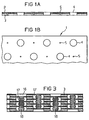
- 1a shows the cross section of such a film 1, which consists of a dielectric Layer 3 and a metallic layer 2 exists. So in principle it represents z.
- To the necessary contacts make certain metal layers to each other can have such a film 1 alternately in the grid large and small recesses 4 and 5 respectively.
- These recesses can be realized as punch holes, for example.
- the Large punch holes 4 can have a diameter, for example of approx. 4 mm and their grid spacing can be between 1 and 2 cm.
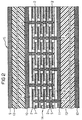
- the foils processed in this way become Intermediate layer 14 made for a printed circuit board 15. This PCB is therefore multi-layered. In the example there is one 4-layer circuit board.
- the layers are metallic Layers 9 to 12 designated.
- Such a circuit board is made up of 2-layer printed circuit boards the metallic layers 9 and 10 and the intermediate Printed circuit board substrate 13 or from the metallic Layers 11 and 12 and the intermediate circuit board substrate 14 are made.
- the layers 10 or 11 to the inner layers mentioned via which the power supply for the assembly elements of such a circuit board he follows.
- the inner layer 10, which is also in a certain way can be structured, e.g. the supply of the voltage potential, while the inner layer 11 of the supply of "Ground potential" serves.
- the film material becomes too processed a capacitive intermediate layer 14 that - connected to the metallic surfaces of the inner layers 10 and 11, respectively, represents a "capacitor" with extensive area.
- the intermediate layer 14 is formed in such a way that a plurality of foils formed according to FIG. 1b are offset are placed on top of each other so that small (5) and large (4) Holes - which are created, for example, by a punching process will always alternate.
- This package can be provided with small holes at the top and bottom Insulating film 7 or 8 may be covered.
- the connection the even-numbered or the odd-numbered metallic Layers can be done, for example, by spot soldering of the foils are made at the small holes.
- the metallic Layers of the individual foils on the small ones soldered together.
- a soldering and contact-enhancing agent e.g. B. the so-called reflow solder paste can be applied.
- the Spot soldering can be done, for example, with the help of a laser beam be performed.
- the larger punch hole prevents that the contact to the respective unaffected metallic Layer occurs.
- the intermediate layer 14 is an independent unit from the to ensure the Metallic contact both upwards and downwards Protrude contact points from the surface.
- the recesses lie to form the intermediate layer of all even and those of all odd Foils are aligned one above the other so that a suitable one can be used Connection technology a contacting of all even numbers metallic layers on the one hand and all odd-numbered ones metallic layers on the other hand is achieved.
- Intermediate layer 14 are the even-numbered metallic Layers with an inner layer 10 and the odd number metallic layers with the other inner layer 11 electrically conductively connected.
- the determination of the even number or odd-numbered metallic layers are starting out from one and the same inner layer, e.g. B. the inner layer 10 made towards other inner layer.
- FIG. 2 shows a circuit board with a single intermediate layer 14 shown.
- Such an intermediate layer 14 can then be placed on inner layers be trained and introduced in the same way.
- 6-layer circuit board would then between the two additional inner layers also the high-capacity intermediate layer be provided.
- FIG. 3 shows a section of a high-capacity intermediate layer shown at the alternate connection the metallic foils among themselves, these foils another Have preprocessing.
- One is the metallic layer and the recess 16, -z relating to the dielectric layer.
- B realized in the form of a corresponding punch hole follows in each case a recess 17, from which only affects the dielectric layer.
- These preprocessed Foils are used to form the intermediate layer overlapping, aligned and aligned.
- a hole-shaped Recess 16 is approximately the same in terms of area Recess 17 opposite, which however only affects the dielectric. Starting from the top, each is an odd number Layer and every even-numbered layer can be connected to each other, since there are only the relevant metallic surface sections face each other.
- the real connection that is symbolically indicated by the "row of pearls" 18 then done by a welding process.
- the removal of the dielectric layer can e.g. B. by using one of these Layer dissolving in the area of the desired recess Be made by means. A removal of this layer could also be done by laser exposure.
Landscapes
- Engineering & Computer Science (AREA)
- Microelectronics & Electronic Packaging (AREA)
- Production Of Multi-Layered Print Wiring Board (AREA)
Applications Claiming Priority (2)
| Application Number | Priority Date | Filing Date | Title |
|---|---|---|---|
| DE19743242 | 1997-09-30 | ||
| DE19743242 | 1997-09-30 |
Publications (2)
| Publication Number | Publication Date |
|---|---|
| EP0906004A2 true EP0906004A2 (fr) | 1999-03-31 |
| EP0906004A3 EP0906004A3 (fr) | 2000-12-13 |
Family
ID=7844178
Family Applications (1)
| Application Number | Title | Priority Date | Filing Date |
|---|---|---|---|
| EP98115620A Withdrawn EP0906004A3 (fr) | 1997-09-30 | 1998-08-19 | Panneau à circuit multicouche |
Country Status (1)
| Country | Link |
|---|---|
| EP (1) | EP0906004A3 (fr) |
Cited By (1)
| Publication number | Priority date | Publication date | Assignee | Title |
|---|---|---|---|---|
| WO2001039562A1 (fr) * | 1999-11-23 | 2001-05-31 | Sun Microsystems, Inc. | Carte de circuit imprime dans laquelle un reseau de distribution d'energie a pertes est utilise pour reduire les resonances au niveau des plans de puissance |
Family Cites Families (1)
| Publication number | Priority date | Publication date | Assignee | Title |
|---|---|---|---|---|
| EP0451541B1 (fr) * | 1990-04-05 | 1995-06-28 | Dyconex AG | Fabrication de plaques de circuit multicouches à densité de conducteurs augmentée |
-
1998
- 1998-08-19 EP EP98115620A patent/EP0906004A3/fr not_active Withdrawn
Cited By (3)
| Publication number | Priority date | Publication date | Assignee | Title |
|---|---|---|---|---|
| WO2001039562A1 (fr) * | 1999-11-23 | 2001-05-31 | Sun Microsystems, Inc. | Carte de circuit imprime dans laquelle un reseau de distribution d'energie a pertes est utilise pour reduire les resonances au niveau des plans de puissance |
| US6441313B1 (en) | 1999-11-23 | 2002-08-27 | Sun Microsystems, Inc. | Printed circuit board employing lossy power distribution network to reduce power plane resonances |
| US6753481B2 (en) | 1999-11-23 | 2004-06-22 | Sun Microsystems, Inc. | Printed circuit board employing lossy power distribution network to reduce power plane resonances |
Also Published As
| Publication number | Publication date |
|---|---|
| EP0906004A3 (fr) | 2000-12-13 |
Similar Documents
| Publication | Publication Date | Title |
|---|---|---|
| DE19911731C2 (de) | Gedruckte Leiterplatte | |
| EP0035093B1 (fr) | Empaquetage pour plusieurs pastilles semiconductrices à commutation rapide | |
| DE4002025C2 (de) | Leiterplatte | |
| DE69800514T2 (de) | Leiterplatte mit primären und sekundären Durchgangslöchern | |
| DE69215192T2 (de) | Leiterplatte mit abgeschirmten bereichen sowie herstellungsverfahren einer solchen leiterplatte | |
| EP1110277B1 (fr) | Ensemble plaquette de circuit imprime a connecteur enfichable multipolaire | |
| DE2911620C2 (de) | Verfahren zum Herstellen von leitenden durchgehenden Bohrungen in Schaltungsplatten | |
| DE69016441T2 (de) | Mehrschichtleiterplatte, welche hochfrequenzinterferenzen von hochfrequenzsignalen unterdrückt. | |
| DE102008032979B4 (de) | Elektromagnetische Bandgap-Struktur, diese umfassende Leiterplatte und Herstellungsverfahren | |
| DE69934814T2 (de) | Nichtzirkuläre mikro-bohrung | |
| DE3020196C2 (de) | Mehrebenen-Leiterplatte und Verfahren zu deren Herstellung | |
| DE3426278C2 (de) | Leiterplatte | |
| DE10019229A1 (de) | Mehrschichtkondensator | |
| DE4020498C2 (de) | Verfahren zum Herstellen von Multiwire-Leiterplatten mit isolierten Metalleitern und/oder optischen Leitern | |
| DE19619710A1 (de) | LC-Filter | |
| DE19627663C2 (de) | Hybride gedruckte Schaltungsplatine | |
| DE10245688A1 (de) | Mehrschichtkeramikelektronikteil, Elektronikteilaggregat und Verfahren zum Herstellen eines Mehrschichtkeramikelektronikteils | |
| EP0756447B1 (fr) | Circuit de commande pour véhicule | |
| DE3323472A1 (de) | Entkopplungsanordnung fuer eine auf einer leiterplatte angeordnete integrierte schaltung | |
| EP0451541B1 (fr) | Fabrication de plaques de circuit multicouches à densité de conducteurs augmentée | |
| DE4326104A1 (de) | Elektrische Baugruppe | |
| DE4312409B4 (de) | Einstellbarer Kondensator | |
| WO1996020500A1 (fr) | Procede de metallisation d'une puce | |
| DE3525012A1 (de) | Busleiste fuer die oberflaechenmontage | |
| DE3937183A1 (de) | Verfahren zu stoerstrahlungsdaempfung an leiterplatten |
Legal Events
| Date | Code | Title | Description |
|---|---|---|---|
| PUAI | Public reference made under article 153(3) epc to a published international application that has entered the european phase |
Free format text: ORIGINAL CODE: 0009012 |
|
| AK | Designated contracting states |
Kind code of ref document: A2 Designated state(s): DE FR GB IT |
|
| AX | Request for extension of the european patent |
Free format text: AL;LT;LV;MK;RO;SI |
|
| PUAL | Search report despatched |
Free format text: ORIGINAL CODE: 0009013 |
|
| AK | Designated contracting states |
Kind code of ref document: A3 Designated state(s): AT BE CH CY DE DK ES FI FR GB GR IE IT LI LU MC NL PT SE |
|
| AX | Request for extension of the european patent |
Free format text: AL;LT;LV;MK;RO;SI |
|
| 17P | Request for examination filed |
Effective date: 20010122 |
|
| AKX | Designation fees paid |
Free format text: DE FR GB IT |
|
| GRAP | Despatch of communication of intention to grant a patent |
Free format text: ORIGINAL CODE: EPIDOSNIGR1 |
|
| STAA | Information on the status of an ep patent application or granted ep patent |
Free format text: STATUS: THE APPLICATION IS DEEMED TO BE WITHDRAWN |
|
| 18D | Application deemed to be withdrawn |
Effective date: 20050802 |