EP0907955B1 - Schieberegister-flashseitenpuffer mit mehreren bits pro zelle - Google Patents
Schieberegister-flashseitenpuffer mit mehreren bits pro zelle Download PDFInfo
- Publication number
- EP0907955B1 EP0907955B1 EP97905795A EP97905795A EP0907955B1 EP 0907955 B1 EP0907955 B1 EP 0907955B1 EP 97905795 A EP97905795 A EP 97905795A EP 97905795 A EP97905795 A EP 97905795A EP 0907955 B1 EP0907955 B1 EP 0907955B1
- Authority
- EP
- European Patent Office
- Prior art keywords
- page buffer
- latch
- output
- logic
- bit line
- Prior art date
- Legal status (The legal status is an assumption and is not a legal conclusion. Google has not performed a legal analysis and makes no representation as to the accuracy of the status listed.)
- Expired - Lifetime
Links
- 239000000872 buffer Substances 0.000 title claims abstract description 47
- 239000000758 substrate Substances 0.000 description 7
- 238000010586 diagram Methods 0.000 description 6
- 238000000034 method Methods 0.000 description 5
- 239000004065 semiconductor Substances 0.000 description 5
- 101000833350 Homo sapiens Phosphoacetylglucosamine mutase Proteins 0.000 description 3
- 102100024440 Phosphoacetylglucosamine mutase Human genes 0.000 description 3
- 101000583553 Homo sapiens Phosphoglucomutase-1 Proteins 0.000 description 2
- 101001072903 Homo sapiens Phosphoglucomutase-2 Proteins 0.000 description 2
- 102100030999 Phosphoglucomutase-1 Human genes 0.000 description 2
- 102100036629 Phosphoglucomutase-2 Human genes 0.000 description 2
- 239000002784 hot electron Substances 0.000 description 2
- 238000012986 modification Methods 0.000 description 2
- 230000004048 modification Effects 0.000 description 2
- 230000004044 response Effects 0.000 description 2
- 101100293180 Arabidopsis thaliana MYB28 gene Proteins 0.000 description 1
- 230000005689 Fowler Nordheim tunneling Effects 0.000 description 1
- 102100029768 Histone-lysine N-methyltransferase SETD1A Human genes 0.000 description 1
- 101000865038 Homo sapiens Histone-lysine N-methyltransferase SETD1A Proteins 0.000 description 1
- 101100020366 Mus musculus Krtap14 gene Proteins 0.000 description 1
- 108010075750 P-Type Calcium Channels Proteins 0.000 description 1
- 230000005684 electric field Effects 0.000 description 1
- 238000005516 engineering process Methods 0.000 description 1
- 230000006870 function Effects 0.000 description 1
- 238000002347 injection Methods 0.000 description 1
- 239000007924 injection Substances 0.000 description 1
- 238000004519 manufacturing process Methods 0.000 description 1
- 239000000463 material Substances 0.000 description 1
Images


Classifications
-
- G—PHYSICS
- G11—INFORMATION STORAGE
- G11C—STATIC STORES
- G11C11/00—Digital stores characterised by the use of particular electric or magnetic storage elements; Storage elements therefor
- G11C11/56—Digital stores characterised by the use of particular electric or magnetic storage elements; Storage elements therefor using storage elements with more than two stable states represented by steps, e.g. of voltage, current, phase, frequency
- G11C11/5621—Digital stores characterised by the use of particular electric or magnetic storage elements; Storage elements therefor using storage elements with more than two stable states represented by steps, e.g. of voltage, current, phase, frequency using charge storage in a floating gate
- G11C11/5642—Sensing or reading circuits; Data output circuits
-
- G—PHYSICS
- G11—INFORMATION STORAGE
- G11C—STATIC STORES
- G11C11/00—Digital stores characterised by the use of particular electric or magnetic storage elements; Storage elements therefor
- G11C11/56—Digital stores characterised by the use of particular electric or magnetic storage elements; Storage elements therefor using storage elements with more than two stable states represented by steps, e.g. of voltage, current, phase, frequency
- G11C11/5621—Digital stores characterised by the use of particular electric or magnetic storage elements; Storage elements therefor using storage elements with more than two stable states represented by steps, e.g. of voltage, current, phase, frequency using charge storage in a floating gate
- G11C11/5628—Programming or writing circuits; Data input circuits
-
- G—PHYSICS
- G11—INFORMATION STORAGE
- G11C—STATIC STORES
- G11C19/00—Digital stores in which the information is moved stepwise, e.g. shift registers
-
- G—PHYSICS
- G11—INFORMATION STORAGE
- G11C—STATIC STORES
- G11C2211/00—Indexing scheme relating to digital stores characterized by the use of particular electric or magnetic storage elements; Storage elements therefor
- G11C2211/56—Indexing scheme relating to G11C11/56 and sub-groups for features not covered by these groups
- G11C2211/564—Miscellaneous aspects
- G11C2211/5642—Multilevel memory with buffers, latches, registers at input or output
-
- G—PHYSICS
- G11—INFORMATION STORAGE
- G11C—STATIC STORES
- G11C8/00—Arrangements for selecting an address in a digital store
- G11C8/04—Arrangements for selecting an address in a digital store using a sequential addressing device, e.g. shift register, counter
Definitions
- This invention relates generally to floating gate memory devices such as an array of flash electrically erasable programmable read-only memory (EEPROM) cells. More particularly, it relates to a shift register page buffer for use in an array of multiple bits-per-cell flash EEPROM memory cells so as to render page mode programming and reading.
- EEPROM electrically erasable programmable read-only memory
- Flash EPROM electrically erasable EPROMs/EEPROMs
- a plurality of one-transistor flash EEPROM core cells may be formed on a semiconductor substrate in which each cell is comprised of a P-type conductivity substrate, an N-type conductivity source region formed integrally with the substrate, and an N-type conductivity drain region also formed integrally within the substrate.
- a floating gate is separated from the substrate by a thin dielectric layer.
- a second dielectric layer separates a control gate from the floating gate.
- a P-type channel region in the substrate separates the source and drain regions.
- the drain region and the control gate are raised to predetermined potentials above the potential applied to the source region.
- the drain region has applied thereto a voltage V D of approximately +5.5 volts with the control gate V G having a voltage of approximately +12 volts applied thereto.
- V D voltage of approximately +5.5 volts
- V G voltage of approximately +12 volts applied thereto.
- a positive potential e.g., +5 volts
- the control gate is at a negative potential (e.g., -8 volts), and the drain region is allowed to float.
- a strong electric field develops between the floating gate and the source region, and a negative charge is extracted from the floating gate to the source region by way of Fowler-Nordheim tunneling.
- the magnitude of the read current is measured.
- the source region is held at a ground potential (0 volts) and the control gate is held at a potential of about +5 volts.
- the drain region is held at a potential between +1 to +2 volts.
- the reference core cells are embedded and associated with every page in the memory core array so that they can be concurrently programmed when the memory core cells are being programmed in parallel, e.g., 128 bytes at a time.
- a reading circuit responsive to a strobe signal is used to compare the memory cell threshold voltage of the selected memory core cell in a page with each of the reference cell threshold voltages so as to determine which one of the plurality of memory states the selected memory core cell is storing.
- a master bandgap voltage reference generator circuit is used to selectively generate one of a plurality of target memory core cell bit line program-verify voltages, each one corresponding to one of the programmable memory states.
- a switching circuit selectively connects a program current source to the array bit lines containing the selected memory core cells which are to be programmed.
- a sensing logic circuit compares continuously the potential on the array bit line with one of the target bit line program-verify voltages.
- the switching circuit disconnects the program current source so as to inhibit further programming when the potential on the bit line falls below the selected one of the plurality of target bit line program-verify voltages.
- the page buffer of the present invention is utilized in the multiple bits-per-cell EEPROM memory cell array programming and reading techniques described in the aforementioned Serial Nos. 08/688,795 and 08/635,995.
- the output of the latch driven by the sense amplifier of the read circuitry contains the stored information based upon the comparison of the array bit line voltage and a target reference cell bit line voltage. This stored information is later clocked into a shift register of the instant page buffer.
- program logic patterns corresponding to the desired programmable memory states are shifted serially into the shift register, which controls whether to allow programming of the selected memory cell or to inhibit programming of the same.
- a page buffer for use in an array of multiple bits-per-cell flash EEPROM memory cells so as to render page mode programming and reading.
- a sensing circuit is provided for selectively and sequentially comparing bit line voltages with each of the plurality of reference voltages.
- a shift register circuit is responsive to the sensing circuit for sequentially storing either a low or high logic level after each comparison of the bit line voltages with one of the plurality of reference voltages.
- the shift register circuit is formed of a plurality of series-connected latch circuits, each having an input and an output.
- a switching circuit is interconnected between the sensing circuit and the latch circuits and is responsive to a corresponding one of the latch outputs for selectively passing the logic signal from the sensing circuit to the input of the latch means.
- the shift register circuit includes an inhibit program circuit which is responsive to certain outputs of the latch means for generating an inhibit logic signal so as to prevent programming.
- the latch means are loaded with data corresponding to memory state regions to be programmed into the selected memory cells.
- Figure 1 a block diagram of a multiple bits-per-cell semiconductor integrated circuit memory device 10 which includes a shift register page buffer so as to render page mode programming and reading operations in an array of multiple bits-per-cell flash electrically erasable read-only memory (EEPROM) cells of the memory device.
- the shift register page buffer 38 and the remaining portions of the memory device 10 are both wholly formed on a single semi-conductor substrate by known CMOS integrated circuit technology.
- the multiple bits-per-cell semiconductor integrated circuit memory device 10 includes a memory core cell array 12, a row address decoder 14, a column address decoder 16, an address input circuit 18, a Y-pass gate circuit 20, a reference cell array 22, a reference Y-select circuit 24, read circuitry 110, and a bit line pre-charge and current source circuitry 36.
- Address signals Aj are applied externally to the address input circuit 18.
- the row address signals from the address input circuit 18 are fed to the row address decoder 14, and the column address signals thereof are fed to the column address decoder 16.
- the row address decoder 14 selects certain ones of the plurality of word lines in the memory core cell array 12 in response to the row address signals.
- the column address decoder 16 selects one of the pages in the memory core array in response to the column address signals as well as corresponding sets of reference columns associated with the selected page.
- the details of the read circuitry 110 and associated components are described and illustrated in the aforementioned application Serial No. 08/688,795 . Further, the details of the bit line pre-charge and current source circuitry 36 and associated components are described and illustrated in the aforementioned Serial No. 08/635,995.
- the page buffer 38 and extended NOR gate circuitry 40 of the present invention are utilized in conjunction with the programming and reading circuits and techniques in these previously mentioned applications.
- the read circuitry contains the stored information based upon the comparison of the array bit line voltages and the target reference cell bit line voltages, which stored information is later clocked into shift registers of the instant page buffer.
- program logic patterns corresponding to the desired target program states are shifted serially into the shift registers of the page buffer, which controls whether to allow programming of the selected memory cells or to inhibit programming of the same.
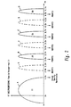
- FIG 2 there is shown a graph of the three reference cell threshold voltages REFVT1, REFVT2, and REFVT3 which serves to divide the programmable threshold range of a two bits-per-cell EEPROM memory cell into four memory state regions (one erased region and three programmable regions).
- the first or erased memory state region is referred to as logic pattern "11.”
- the second or first programmable memory state region is referred to as logic pattern “10.”
- the third or second programmable memory state region is referred to as logic pattern "01.”
- the fourth or third programmable memory state region is referred to as logic pattern "00.”
- the first reference cell threshold voltage REFVT1 separates the logic patterns “11” and “10.”
- the second reference cell threshold voltage REFVT2 separates the logic patterns “10” and "01.”
- the third reference cell threshold voltage REFVT3 separates the logic patterns "01” and "00.”
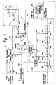
- FIG 3 there is illustrated a simple block diagram of the shift register page buffer 38 of Figure 1 and the portions of the associated circuitry in the read circuitry block 110, bit line pre-charge and current source circuitry block 36, and the extended NOR gate circuit block 40.
- the shift register page buffer 38 is comprised of two series-connected shift register elements 300, a switch circuit portion 310, and an inhibit program circuit portion 312.
- the first shift register 300 is formed of series-connected latches 302 and 304.
- the second shift register 300 is formed of series-connected latches 306 and 308.
- a serial input data line 314 is used to connect the output of a preceding page buffer associated with an adjacent bit line to the input of the first latch 302 in the first shift register 300.
- the output of the first latch 302 on line 316 is connected to the input of the second latch 304 whose output on line 318 is connected to the input of the third latch 306.
- the output of the third latch 306 on line 320 is connected to the input of the fourth latch 308.
- a serial output data line 322 is used to connect the output of the fourth latch 308 to the input of a next succeeding page buffer associated with an adjacent bit line.
- the inhibit program circuit portion 312 has a first input on line 324 connected to the output of the first latch 302 and a second input on line 326 connected to the output of the third latch 306.
- the output of the inhibit program circuit is connected via line 328 to another input of the latch 27 in the read circuitry 110.
- the switch circuit portion 310 has a first terminal on line 330 connected to the output of the latch 27 and a second terminal on line 332 connected also to the output of the third latch 306.
- the switch circuit portion 310 has a third terminal on line 334 which is connected to a second input of the first latch 302.
- the read circuitry 110 contains the differential pair amplifier 26 and the latch 27.
- the differential amplifier 26 has its inverting input connected to a node 336 and to the bit line BL from the memory core cell array 12 and its non-inverting input connected to a line 338 for receiving either a bandgap derived reference voltage BGR or the reference bit line voltage REFBLX.
- the output of the differential pair amplifier 26 is fed to the input of the latch 27 whose output defines the output of the read circuitry 110.
- the output of the latch 27 is fed via line 340 to the input of the bit line pre-charge and current source circuitry 36, via the line 330 to the input of the page buffer 38, and via line 342 to the input of the NOR gate circuitry 40.
- the current source circuitry 36 has a first input on line 344 for receiving the program high voltage VPROG, a second input on line 346 for receiving a read voltage, and a third input on line 348 for receiving a current source enable voltage.
- the output of the current source circuity 36 is on line 350 which is fed to the inverting input of the differential pair amplifier 26 via the node 336.
- the NOR gate circuitry 40 is used for generating a signal VERIFY on line 41 which goes to a high logic level when the whole page has been verified.
- the first latch 302 is formed of a pass transistor N1 and a pair of cross-coupled inverters I1 and I2.
- the second latch 304 is formed of a pass transistor N2 and a pair of cross-coupled inverters I3 and I4.
- the third latch 306 is formed of a pass transistor N3 and a pair of cross-coupled inverters I5 and I6, and the fourth latch 308 is formed of a pass transistor N4 and a pair of cross-coupled inverters I7 and I8.
- the inhibit program circuit portion 312 includes three series-connected P-channel transistors P1, P2 and P3 connected between the power supply potential VCC and the line 328 which is connected to the input of the latch 27.
- the transistor P1 has its source connected to the power supply potential VCC, its gate connected to a program enable signal PE and its drain connected to the source of the transistor P2.
- the transistor P2 has its gate connected to the input of the inverter I7 and its drain connected to the source of the transistor P3.
- the drain of the transistor P3 is connected to the line 328.
- the switch circuit portion 310 is formed of an N-channel transistor N5 having its drain/source conduction path connected between the output of the latch 27 (line 330) and the second input of the first latch 302 (line 334). The gate of the transistor N5 is connected to the input of the inverter I7.
- the differential pair amplifier 26 includes load P-channel transistors P4, P5; input N-channel transistors N6, N7; and a current source transistor N8.
- the gate of the input transistor N6 is connected to receive the voltage on the bit line BL, and the gate of the input transistor N7 is connected to receive the reference voltage BGR/REFBLX.
- the gate of the transistor N8 is connected to a bias voltage V BIAS .
- the latch 27 is comprised of a pair of cross-coupled inverters I9 and I10; P-channel transistor P7; and N-channel transistors N9-N12.
- the bit line pre-charge and current source circuitry 36 includes P-channel transistors P8, P9; N-channel transistors N13-N15; and a 5 ⁇ A current source Is.
- the gate of the transistor N14 defining the input of the current source circuitry 36 on the line 340 is connected to the output of the latch 27.
- the drain of the transistor N14 is connected to the line 350 defining the output of the current source circuitry 36.
- the source of the transistor P8 is connected to the program high voltage VPROG, and the gate of the transistor N15 is connected to the line 348 for receiving the current source enable signal.
- the extended NOR gate circuit block 40 is comprised of a plurality of identical verify circuits 40a, one of which is shown in detail.
- Each of the verify circuits 40a includes series-connected pull-up transistor P10 and pull-down transistor N16.
- the pull-up transistor P10 has its source connected to the power supply potential VCC, its gate connected to a common load signal, and its drain connected to the drain of the pull-down transistor N16.
- the gate of the transistor N16 is connected to the output of the latch 27 via the line 342, and the source thereof is connected to the ground potential.
- the common node 352 of the transistors P10 and N16 is connected to all of the other common nodes in the plurality of verify circuits 40a so as to place them in a parallel arrangement.
- the common node 352 is further connected to the output line 41 so as to produce the signal VERIFY.
- the outputs of all of the latches 302-308 of the shift registers are set to zero.
- the read signal READ on the gate of the transistor N13 will be made high so as to precharge all of the bit lines BL to the same potential (i.e., +1.5 V) prior to the start of the read mode.
- the program high voltage VPROG will be set equal to the power supply potential VCC during the read mode. The read operation is described and illustrated in the aforementioned application Serial No. 08/688,795.
- the second reference threshold level REFVT2 programmed into the corresponding one of the associated reference core cells is selected to be used as the reference voltage REFBLX defining a target reference cell bit line voltage on the line 338. Since the voltage on the bit line corresponding to the third programmable memory state region will be higher than the second reference threshold level REFVT2, the output of the differential pair amplifier 26 will be low and the output of the latch 27 will store a logic "1.”
- the output of the inverter I1 will store a logic "0.” Thereafter, the gate of the transistor N2 will receive the signal CLKB so as to shift the MSB from the output of the first latch 302 (inverter I1) to the output of the second latch 304 (inverter I3).
- a second read step operation is performed by initially precharging again all of the bit lines to the same potential prior to start of the second read mode. Further, the gate of the pass transistor N3 receives the signal CLK so as to further shift the MSB from the output of the second latch 304 to the output of the third latch 306 (inverter I5).
- the first reference threshold level REFVT1 programmed into the corresponding one of the associated reference core cells is selected to be used this time as the reference voltage REFBLX on the line 338.
- the output of the differential pair amplifier 26 will again be low and the output of the latch 27 will store a logic "1.” Again, the output of the latch 27 is transferred into the first latch 302 by the transistor N5. Thus, the output of the inverter I1 will store a logic "0.” Thereafter, the gate of the pass transistors N2 and N4 will receive the signal CLKB so as to shift the MSB from the output of the third latch 306 (inverter I5) to the output of the fourth latch 308 (inverter I7) and to shift result of the second read step stored in the first latch to the second latch.
- a third read step is performed by initially pre-charging once again all of the bit lines to the same potential prior to the start of the third read mode.
- the third reference threshold level REFVT3 programmed into the corresponding one of the associated reference core cells is selected to be used this time as the reference voltage REFBLX on the line 338. Since the bit line voltage corresponding to the third programmed memory state region will be higher than the third reference threshold level REFVT3, the output of the differential pair amplifier 26 will be low and the output of the latch 27 will store a logic "1.”
- the least significant bit is shifted from the first latch 302 to the second latch 304.
- the outputs of the first and second latches 302, 304 will be storing the LSB, and the outputs of the third and fourth latches 306, 308 will be storing the MSB.
- the data or logic pattern "stored in the latches" will be shifted serially out from the shift registers via the serial data output line 322 after the whole page has been read.
- the signal SET1 on the gate of the transistor N18 is made high.
- the logic "0" at the output of the inverter I1 is passed through to the input of the inverter I7 by clocking the signals CLK and CLKB. This causes the output of the latch 27 on the line 340 to go low ("0").
- the corresponding bit line BL on the page is pre-charged by the program inhibit high voltage VPROG (approximately 5-6 V) via the transistors P8 and P9.
- VPROG approximately 5-6 V
- the common array ground line VSS is also charged to the same high voltage.
- a page of data to be programmed is loaded serially into the page buffers 38 associated with the bit lines in the page through the serial input data line 314.
- the first and second latches 302, 304 are loaded with "0,” and the third and fourth latches are also loaded with “0.” Then signal REL will go high so as to cause the output of the latch 27 to go high ("1"). Consequently, the current source will be switched on due to the conduction of the transistor N14.
- the programming will begin when the voltage on the word line WL 1 is charged up to the voltage VPP. However, if the page buffer 38 is loaded with "11" data (the outputs of the inverters I3 and I7) corresponding to the erased memory state region, then the inhibit programming circuit 312 will cause the output of the latch 27 to be switched to the logic "0" corresponding to a verified state. Accordingly, the current source will be turned off and no programming will occur.
- an external logic controller 354 will cause the first target program memory state level PGM1 to be set or applied as the reference voltage BGR to the gate of the input transistor N7.
- the memory cell MC 11 will be charging or programming until the bit line voltage falls below the first reference memory programmed state level PMG1.
- the output of the differential pair amplifier 26 will go high and the output of the latch 27 will be switched to a logic "0,” thereby turning off the current source I s and charging the bit line back to the program high voltage VPROG. This is the program inhibit state.
- the external logic controller 354 will cause the second reference programmed memory state level PGM2 to be applied as a reference voltage BGR to the gate of the transistor N7. Thereafter, the memory cell MC 11 will continue to program until the bit line voltage falls below the second reference program memory state level. At that time, the latch 27 will again be switched to a logic "0" in order to switch off the current source and further programming. The bit line voltage will again be charged back to the program inhibit high voltage VPROG. After all of the bit lines in the page that are to be programmed to the second program memory state region (logic pattern "01"), then the output signal VERIFY on the line 41 will go high. The memory cells that are not required to be programmed beyond the second level are inhibited.
- the external logic controller 354 will load the shift register with the next set of data (i.e., logic "10") which causes the third reference program memory state level PGM3 to be applied as the reference voltage BGR to the gate of the input transistor N7. Consequently, the memory cell MC 11 will continue to program until the bit line voltage falls below the third reference programmed memory state level. At that time, the latch 27 will again be switched to a logic "0" in order to switch off the current source and inhibit further programming. The bit line will again be charged back to the program high voltage VPROG. Lastly, after all of the bit lines in the page that are to be programmed to the third program memory state region (logic pattern "00"), then the output signal VERIFY on the line 41 will go high. The signal ISO on the gate of the transistor N17 serves to isolate the shift register from the latch 27 during programming.
- the next set of data i.e., logic "10"
- the present invention provides a shift register page buffer for use in an array of multiple bits-per-cell flash EEPROM memory cells so as to render page mode programming and reading.
- a sensing logic circuit is provided for selectively and sequentially comparing the array bit line voltages with a plurality of target reference cell bit line voltages.
- a shift register circuit is responsive to the sensing circuit for sequentially storing either a low or high logic level after each comparison of the bit line voltages with each of the plurality of target cell bit line reference voltages.
- the shift register circuit is formed of series-connected latch circuits having inputs and outputs.
Landscapes
- Engineering & Computer Science (AREA)
- Computer Hardware Design (AREA)
- Read Only Memory (AREA)
Claims (13)
- Seitenpuffer zur Verwendung für ein Array pro Zelle mehrere Bits aufweisender Flash-EEPROM-Speicherzellen zwecks Ermöglichung eines Seitenmodus-Programmierens und -Lesens, wobei der Seitenpuffer in Kombination aufweist:eine Abtastlogikeinrichtung (26,27) zum selektiven und sequentiellen Vergleichen von Array-Bitleitungs-Spannungen mit jeder von mehreren Ziel-Referenzzellen-Bitleitungs-Spannungen;eine Schieberegistereinrichtung (300), die in Reaktion auf die Abtastlogikschaltungseinrichtung nach jedem Vergleich der Bitleitungs-Spannungen mit einer der mehreren Ziel-Referenzzellen-Bitleitungs-Spannungen sequentiell entweder einen Low- oder einen High-Logikpegel speichert, wobei die Schieberegistereinrichtung in Reihe geschaltete Haltespeichereinrichtungen (302-308) aufweist, die jeweils mit Eingängen und Ausgängen versehen sind; undeine Verknüpfungs-Schaltungseinrichtung (N5), die zwischen die Abtastlogikeinrichtung und die Haltespeichereinrichtung (302) geschaltet ist und auf eines der Haltespeichereinrichtungs-Ausgangssignale hin selektiv das Logik-Signal (342) aus der Abtastlogikeinrichtung dem Eingang der Haltespeichereinrichtungen zuführt.
- Seitenpuffer nach Anspruch 1, bei dem jede der Haltespeichereinrichtungen (302-308) einen ersten Inverter und einen zweiten Inverter aufweist, wobei der Eingang des ersten Inverters mit dem Ausgang des zweiten Inverters verbunden ist und sein Ausgang mit dem Eingang des zweiten Inverters verbunden ist.
- Seitenpuffer nach Anspruch 2, bei dem die Verknüpfungs-Schaltungseinrichtung einen Schalttransistor (N5) aufweist, dessen Drain mit dem Ausgang der Abtastlogikeinrichtung verbunden ist, dessen Source mit der Haltespeichereinrichtung verbunden ist und dessen Gate mit einem Ausgang einer der Halteeinrichtungen verbunden ist.
- Seitenpuffer nach Anspruch 3, bei dem die Abtastlogikschaltungseinrichtung einen Differentialverstärker (26), der als Komparator funktioniert, und einen Haltespeicher (27) aufweist.
- Seitenpuffer nach Anspruch 4, bei dem die Komparatoreinrichtung einen ersten Eingang, der derart geschaltet ist, daß er die Bitleitungs-Spannungen empfängt, und einen zweiten Eingang aufweist, der derart geschaltet ist, daß er die mehreren Ziel-Referenzzellen-Bitleitungs-Spannungen empfängt.
- Seitenpuffer nach Anspruch 5, bei dem die Komparatoreinrichtung eine Abtastverstärkungseinrichtung aufweist.
- Seitenpuffer nach Anspruch 6, bei dem die Abtastverstärkungseinrichtung einen invertierenden Eingang, der den ersten Eingang der Komparatoreinrichtung bildet, einen nichtinvertierenden Eingang aufweist, der den zweiten Eingang der Komparatoreinrichtung bildet, und einen Ausgang aufweist, wobei der Haltespeicher (27) mit seinem Eingang mit dem Ausgang der Abtastverstärkungseinrichtung verbunden ist, und einen Ausgang zum Ausgeben des Logik-Signals (342) aufweist.
- Seitenpuffer nach Anspruch 7, bei dem der Ausgang des Haltespeichers (27) mit einem Ausgangsanschluß zum Ausgeben des Logik-Signals (342) verbunden ist.
- Seitenpuffer nach Anspruch 1, ferner mit einer Programmierungsverhinderungs-Schaltungseinrichtung (312), die während eines Programmier-Modus auf Ausgangssignale der Haltespeichereinrichtung (302) hin ein Verhinderungs-Logiksignal (328) erzeugt, mittels dessen das Logik-Signal (342) aus der Abtastlogikschaltungseinrichtung (26) einen Low-Logikpegel führt, um dadurch ein Programmieren zu verhindern.
- Seitenpuffer nach Anspruch 9, bei dem die Haltespeichereinrichtung (302) mit Daten geladen wird, die Speicherzustandsbereichen entsprechen, die während des Programmier-Modus in die gewählten Speicherzellen programmiert werden sollen, und ferner eine externe Logiksteuereinrichtung (354) aufweist, um selektiv eine der mehreren Ziel-Referenzzellen-Bitleitungs-Spannungen auszugeben.
- Seitenpuffer nach Anspruch 10, ferner mit einer Logikgattereinrichtung (40), die auf das Logik-Signal (342) hin ein Verifizierungssignal (41) erzeugt, wenn die Abtastlogikschaltungseinrichtung einen Vergleich der ganzen Seite abgeschlossen hat.
- Seitenpuffer nach Anspruch 11, ferner mit einer Stromquellenschaltungseinrichtung (36) zum selektiven Verbinden einer Programmierstromquelle und Zufuhr aus dieser mit bzw. zu der Bitleitung, wenn das Ausgangssignal der Abtastlogikschaltungseinrichtung sich auf dem High-Logikpegel befindet, und zum Trennen der Programmierstromquelle, wenn das Ausgangssignal der Abtastlogikschaltungseinrichtung sich auf dem Low-Logikpegel befindet.
- Seitenpuffer nach einem der vorhergehenden Ansprüche, bei dem die pro Zelle mehrere Bits aufweisenden Speicherzellen Speicherzellen für zwei Bits pro Zelle sind.
Applications Claiming Priority (3)
| Application Number | Priority Date | Filing Date | Title |
|---|---|---|---|
| US669116 | 1996-06-24 | ||
| US08/669,116 US5724284A (en) | 1996-06-24 | 1996-06-24 | Multiple bits-per-cell flash shift register page buffer |
| PCT/US1997/001874 WO1997050090A1 (en) | 1996-06-24 | 1997-01-31 | A multiple bits-per-cell flash shift register page buffer |
Publications (2)
| Publication Number | Publication Date |
|---|---|
| EP0907955A1 EP0907955A1 (de) | 1999-04-14 |
| EP0907955B1 true EP0907955B1 (de) | 2000-05-31 |
Family
ID=24685094
Family Applications (1)
| Application Number | Title | Priority Date | Filing Date |
|---|---|---|---|
| EP97905795A Expired - Lifetime EP0907955B1 (de) | 1996-06-24 | 1997-01-31 | Schieberegister-flashseitenpuffer mit mehreren bits pro zelle |
Country Status (5)
| Country | Link |
|---|---|
| US (1) | US5724284A (de) |
| EP (1) | EP0907955B1 (de) |
| DE (1) | DE69702195T2 (de) |
| TW (1) | TW364997B (de) |
| WO (1) | WO1997050090A1 (de) |
Families Citing this family (25)
| Publication number | Priority date | Publication date | Assignee | Title |
|---|---|---|---|---|
| US5973967A (en) * | 1997-01-03 | 1999-10-26 | Programmable Microelectronics Corporation | Page buffer having negative voltage level shifter |
| US5933370A (en) * | 1998-01-09 | 1999-08-03 | Information Storage Devices, Inc. | Trimbit circuit for flash memory |
| US6065760A (en) * | 1998-07-06 | 2000-05-23 | Weygandt; James H. | Interchangeable skate wheel bearing assembly |
| US6002611A (en) * | 1998-07-22 | 1999-12-14 | Halo Lsi Design & Device Technology, Inc. | Fast, low current program with auto-program for flash memory |
| KR100319559B1 (ko) * | 1999-11-01 | 2002-01-05 | 윤종용 | 문턱 전압 분포들 사이의 마진을 일정하게 유지할 수 있는멀티-스테이트 불휘발성 반도체 메모리 장치 |
| FR2803080A1 (fr) * | 1999-12-22 | 2001-06-29 | St Microelectronics Sa | Memoire flash programmable page par page |
| US7056123B2 (en) * | 2001-07-16 | 2006-06-06 | Immersion Corporation | Interface apparatus with cable-driven force feedback and grounded actuators |
| US7042770B2 (en) | 2001-07-23 | 2006-05-09 | Samsung Electronics Co., Ltd. | Memory devices with page buffer having dual registers and method of using the same |
| US6621739B2 (en) * | 2002-01-18 | 2003-09-16 | Sandisk Corporation | Reducing the effects of noise in non-volatile memories through multiple reads |
| US6836432B1 (en) * | 2002-02-11 | 2004-12-28 | Advanced Micro Devices, Inc. | Partial page programming of multi level flash |
| US6901498B2 (en) * | 2002-12-09 | 2005-05-31 | Sandisk Corporation | Zone boundary adjustment for defects in non-volatile memories |
| US6775184B1 (en) * | 2003-01-21 | 2004-08-10 | Nexflash Technologies, Inc. | Nonvolatile memory integrated circuit having volatile utility and buffer memories, and method of operation thereof |
| US7023735B2 (en) * | 2003-06-17 | 2006-04-04 | Ramot At Tel-Aviv University Ltd. | Methods of increasing the reliability of a flash memory |
| DE602004010239T2 (de) * | 2004-05-20 | 2008-09-25 | Stmicroelectronics S.R.L., Agrate Brianza | Verbesserter Seitenspeicher für eine programmierbare Speichervorrichtung |
| KR100609568B1 (ko) * | 2004-07-15 | 2006-08-08 | 에스티마이크로일렉트로닉스 엔.브이. | 비휘발성 메모리 장치의 페이지 버퍼 및 이를 이용한프로그램 방법과 독출 방법 |
| KR100680478B1 (ko) * | 2005-03-22 | 2007-02-08 | 주식회사 하이닉스반도체 | 면적이 감소된 플래시 메모리 장치와 그 액세스 제어 방법 |
| KR100778082B1 (ko) | 2006-05-18 | 2007-11-21 | 삼성전자주식회사 | 단일의 래치 구조를 갖는 멀티-비트 플래시 메모리 장치,그것의 프로그램 방법, 그리고 그것을 포함하는 메모리카드 |
| US7876613B2 (en) | 2006-05-18 | 2011-01-25 | Samsung Electronics Co., Ltd. | Multi-bit flash memory devices having a single latch structure and related programming methods, systems and memory cards |
| KR100919156B1 (ko) | 2006-08-24 | 2009-09-28 | 삼성전자주식회사 | 멀티-비트 플래시 메모리 장치 및 그것의 프로그램 방법 |
| KR100769770B1 (ko) * | 2006-09-29 | 2007-10-23 | 주식회사 하이닉스반도체 | 메모리 장치의 페이지 버퍼 회로 및 프로그램 방법 |
| US8284749B2 (en) * | 2008-03-10 | 2012-10-09 | Comtech Mobile Datacom Corporation | Time slot synchronized, flexible bandwidth communication system |
| US8245515B2 (en) * | 2008-08-06 | 2012-08-21 | General Electric Company | Transition duct aft end frame cooling and related method |
| WO2011062058A1 (en) * | 2009-11-20 | 2011-05-26 | Semiconductor Energy Laboratory Co., Ltd. | Semiconductor device |
| KR101126514B1 (ko) * | 2009-12-31 | 2012-03-29 | 주식회사 하이닉스반도체 | 반도체 메모리 장치 및 그 독출 방법 |
| US8416624B2 (en) | 2010-05-21 | 2013-04-09 | SanDisk Technologies, Inc. | Erase and programming techniques to reduce the widening of state distributions in non-volatile memories |
Family Cites Families (7)
| Publication number | Priority date | Publication date | Assignee | Title |
|---|---|---|---|---|
| KR910009588B1 (ko) * | 1987-05-06 | 1991-11-21 | 니뽄 덴끼 가부시끼가이샤 | 직렬 어드레싱 회로를 갖는 직렬 억세스 메모리 회로 |
| US5200925A (en) * | 1988-07-29 | 1993-04-06 | Mitsubishi Denki Kabushiki Kaisha | Serial access semiconductor memory device and operating method therefor |
| US5198999A (en) * | 1988-09-12 | 1993-03-30 | Kabushiki Kaisha Toshiba | Serial input/output semiconductor memory including an output data latch circuit |
| US5172338B1 (en) * | 1989-04-13 | 1997-07-08 | Sandisk Corp | Multi-state eeprom read and write circuits and techniques |
| US5218569A (en) * | 1991-02-08 | 1993-06-08 | Banks Gerald J | Electrically alterable non-volatile memory with n-bits per memory cell |
| JP2554816B2 (ja) * | 1992-02-20 | 1996-11-20 | 株式会社東芝 | 半導体記憶装置 |
| JPH08115598A (ja) * | 1994-10-18 | 1996-05-07 | Mitsubishi Denki Semiconductor Software Kk | 不揮発性半導体記憶装置及び半導体装置 |
-
1996
- 1996-06-24 US US08/669,116 patent/US5724284A/en not_active Expired - Lifetime
-
1997
- 1997-01-31 EP EP97905795A patent/EP0907955B1/de not_active Expired - Lifetime
- 1997-01-31 WO PCT/US1997/001874 patent/WO1997050090A1/en not_active Ceased
- 1997-01-31 DE DE69702195T patent/DE69702195T2/de not_active Expired - Lifetime
- 1997-02-05 TW TW086101386A patent/TW364997B/zh active
Also Published As
| Publication number | Publication date |
|---|---|
| WO1997050090A1 (en) | 1997-12-31 |
| DE69702195T2 (de) | 2001-02-22 |
| US5724284A (en) | 1998-03-03 |
| DE69702195D1 (de) | 2000-07-06 |
| EP0907955A1 (de) | 1999-04-14 |
| TW364997B (en) | 1999-07-21 |
Similar Documents
| Publication | Publication Date | Title |
|---|---|---|
| EP0907955B1 (de) | Schieberegister-flashseitenpuffer mit mehreren bits pro zelle | |
| KR100256616B1 (ko) | 불휘발성 반도체 기억장치 | |
| US6031760A (en) | Semiconductor memory device and method of programming the same | |
| US5371705A (en) | Internal voltage generator for a non-volatile semiconductor memory device | |
| US6788601B2 (en) | Semiconductor memory device and current mirror circuit | |
| JP3373632B2 (ja) | 不揮発性半導体記憶装置 | |
| EP0922285B1 (de) | Löschverfahren für mehrere-bits-pro-zelle flash -eeprom mit seitenmodus | |
| US6525960B2 (en) | Nonvolatile semiconductor memory device including correction of erratic memory cell data | |
| US4937787A (en) | Programmable read only memory with means for discharging bit line before program verifying operation | |
| US5748536A (en) | Data read circuit for a nonvolatile semiconductor memory | |
| US4933906A (en) | Non-volatile semiconductor memory device | |
| US20030202392A1 (en) | Nonvolatile memory and method of programming the same memory | |
| US5798967A (en) | Sensing scheme for non-volatile memories | |
| EP0211232B1 (de) | Halbleiterspeicher mit einem Leseverfahren in einem grossen Speisespannungsbereich | |
| US5982662A (en) | Semiconductor memory device with improved read characteristics for data having multi values | |
| US6477092B2 (en) | Level shifter of nonvolatile semiconductor memory | |
| TW201921369A (zh) | 用於讀取快閃記憶體單元中的資料的經改善感測放大器電路 | |
| US6147910A (en) | Parallel read and verify for floating gate memory device | |
| US5400287A (en) | Method for erasing and verifying nonvolatile semiconductor memory device | |
| US5402382A (en) | Nonvolatile semiconductor memory device capable of erasing by a word line unit | |
| KR102194907B1 (ko) | 반도체 기억장치 및 독출 방법 | |
| US20020054506A1 (en) | Nonvolatile semiconductor memory device and data writing method therefor | |
| JPH11110985A (ja) | 不揮発性半導体記憶装置およびその書き込み方法 | |
| US6166957A (en) | Nonvolatile semiconductor memory device with a level shifter circuit | |
| US7512020B2 (en) | Nonvolatile memory device with load-free wired-OR structure and an associated driving method |
Legal Events
| Date | Code | Title | Description |
|---|---|---|---|
| PUAI | Public reference made under article 153(3) epc to a published international application that has entered the european phase |
Free format text: ORIGINAL CODE: 0009012 |
|
| 17P | Request for examination filed |
Effective date: 19981019 |
|
| AK | Designated contracting states |
Kind code of ref document: A1 Designated state(s): DE GB |
|
| RIN1 | Information on inventor provided before grant (corrected) |
Inventor name: SU, JONATHAN, SHICHANG Inventor name: ZHOU, QIMENG (DEREK) Inventor name: GUTALA, RAVI, PRAKASH Inventor name: BILL, COLIN, STEWART |
|
| GRAG | Despatch of communication of intention to grant |
Free format text: ORIGINAL CODE: EPIDOS AGRA |
|
| 17Q | First examination report despatched |
Effective date: 19990917 |
|
| GRAG | Despatch of communication of intention to grant |
Free format text: ORIGINAL CODE: EPIDOS AGRA |
|
| GRAH | Despatch of communication of intention to grant a patent |
Free format text: ORIGINAL CODE: EPIDOS IGRA |
|
| GRAH | Despatch of communication of intention to grant a patent |
Free format text: ORIGINAL CODE: EPIDOS IGRA |
|
| GRAA | (expected) grant |
Free format text: ORIGINAL CODE: 0009210 |
|
| AK | Designated contracting states |
Kind code of ref document: B1 Designated state(s): DE GB |
|
| REF | Corresponds to: |
Ref document number: 69702195 Country of ref document: DE Date of ref document: 20000706 |
|
| EN | Fr: translation not filed | ||
| PLBE | No opposition filed within time limit |
Free format text: ORIGINAL CODE: 0009261 |
|
| STAA | Information on the status of an ep patent application or granted ep patent |
Free format text: STATUS: NO OPPOSITION FILED WITHIN TIME LIMIT |
|
| 26N | No opposition filed | ||
| REG | Reference to a national code |
Ref country code: GB Ref legal event code: IF02 |
|
| REG | Reference to a national code |
Ref country code: GB Ref legal event code: 732E |
|
| REG | Reference to a national code |
Ref country code: GB Ref legal event code: 732E |
|
| PGFP | Annual fee paid to national office [announced via postgrant information from national office to epo] |
Ref country code: GB Payment date: 20071212 Year of fee payment: 12 |
|
| GBPC | Gb: european patent ceased through non-payment of renewal fee |
Effective date: 20090131 |
|
| PG25 | Lapsed in a contracting state [announced via postgrant information from national office to epo] |
Ref country code: GB Free format text: LAPSE BECAUSE OF NON-PAYMENT OF DUE FEES Effective date: 20090131 |
|
| REG | Reference to a national code |
Ref country code: DE Ref legal event code: R082 Ref document number: 69702195 Country of ref document: DE Representative=s name: MURGITROYD & COMPANY, DE Ref country code: DE Ref legal event code: R081 Ref document number: 69702195 Country of ref document: DE Owner name: CYPRESS SEMICONDUCTOR CORP. (N.D.GES.D.STAATES, US Free format text: FORMER OWNER: SPANSION LLC (N.D.GES.D. STAATES DELAWARE), SUNNYVALE, CALIF., US |
|
| PGFP | Annual fee paid to national office [announced via postgrant information from national office to epo] |
Ref country code: DE Payment date: 20160725 Year of fee payment: 20 |
|
| REG | Reference to a national code |
Ref country code: DE Ref legal event code: R071 Ref document number: 69702195 Country of ref document: DE |