EP0908734A2 - Elektrooptisches Sampling-Oszilloskop - Google Patents
Elektrooptisches Sampling-Oszilloskop Download PDFInfo
- Publication number
- EP0908734A2 EP0908734A2 EP98308133A EP98308133A EP0908734A2 EP 0908734 A2 EP0908734 A2 EP 0908734A2 EP 98308133 A EP98308133 A EP 98308133A EP 98308133 A EP98308133 A EP 98308133A EP 0908734 A2 EP0908734 A2 EP 0908734A2
- Authority
- EP
- European Patent Office
- Prior art keywords
- optical
- optical pulse
- circuit
- timing
- electro
- Prior art date
- Legal status (The legal status is an assumption and is not a legal conclusion. Google has not performed a legal analysis and makes no representation as to the accuracy of the status listed.)
- Withdrawn
Links
Images




Classifications
-
- G—PHYSICS
- G01—MEASURING; TESTING
- G01R—MEASURING ELECTRIC VARIABLES; MEASURING MAGNETIC VARIABLES
- G01R13/00—Arrangements for displaying electric variables or waveforms
- G01R13/20—Cathode-ray oscilloscopes
- G01R13/22—Circuits therefor
- G01R13/34—Circuits for representing a single waveform by sampling, e.g. for very high frequencies
- G01R13/347—Circuits for representing a single waveform by sampling, e.g. for very high frequencies using electro-optic elements
Definitions
- the present invention relates to an electro-optic sampling oscilloscope, in which an electric field generated by a signal to be measured is coupled to an electro-optic crystal, an optical pulse is caused to enter this electro-optic crystal, and the waveform of the signal to be measured is observed by means of the polarization state of the optical pulse.
- the present invention relates to an electro-optic sampling oscilloscope that is provided with characteristic features in the generation of the optical pulse.
- EOS electro-optic sampling oscilloscope
- Figure 5 serves to explain the measurement concept of the electro-optic probe in an EOS oscilloscope.
- a metal pin 21 is provided at the lead end of the electro-optic probe, and by placing this in contact with the signal line 31 which is the subject of measurement, an electric field 23 is generated based on the measured signal.
- the electro-optic crystal 22 is provided at the end of the metal pin 21.
- the index of refraction of the electro-optic crystal changes in accordance with the coupled electric field strength, so that when an optical pulse 25 is inputted in this state, the polarization state of the optical pulse changes.
- the optical pulse 25 which experiences a change in polarization is reflected by reflection mirror 24, which is a multi-layered dielectric film mirror, and is guided to the light receiver 26, which serves as the input part of the polarization detecting optical system within the electro-optic probe (Shinagawa, et al: ""A High-Impedance Probe Based on Electo-Optic Sampling,” Proceeding of the 15 th Meeting on Lightwave Sensing Technology, May 1995, pp 123-129).
- the EOS oscilloscope comprises an EOS oscilloscope main body 1 and an electro-optic probe 2.
- the optical pulse 25 explained in the discussion of Figure 5 is generated in the optical pulse output circuit 4 on the basis of the trigger signal from a trigger circuit 3, and is supplied to the electro-optic probe 2. Additionally, once the optical pulse has experienced a change in polarization, the detection of the polarization thereof and the like are conducted by the polarization detecting optical system (not depicted in the figure) within the electro-optic probe 2, and the signal thereof is inputted into the EOS oscilloscope main body 1. Additionally, the amplification and A/D conversion of the signal are conducted by A/D circuit 5, and processing in order to display the signal which is the subject of measurement, and the like, is conducted by processing circuit 6.
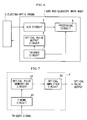
- FIG 7 shows the details of the optical pulse output circuit 4 in Figure 6.
- timing circuit 31 generates a timing signal, which is the optical pulse generating timing, based on the trigger signal from trigger circuit 3.
- optical pulse generating circuit 32 generates a sample optical pulse based on the timing signal of timing circuit 31. Since the amount of light is insufficient with this sample optical pulse, the sample optical pulse is optically amplified by optical amplifier circuit 33, and the output of this optical amplifier circuit 33 is supplied to electro-optic probe 2 as an optical pulse.
- ASE Amplified Spontaneous Emitting
- spontaneously emitted light which is unnecessary and does not contribute to sampling in the spectrum or to sampling along the time axis
- Figure 8 shows an example of the spectral analysis of output from the optical amplifier circuit 33 in the optical pulse output circuit 4 shown in Figure 7.
- a sample optical pulse is outputted from the optical pulse generating circuit 32 which has essentially a single frequency, and light having other frequencies, which constitutes noise, is at a sufficiently low level that it can be ignored; however, light which is unnecessary and does not contribute to the sampling in the spectra is generated by optical amplifier circuit 33, so that light having frequencies other than the frequency outputted by the optical pulse generating circuit 32 is also outputted, and reaches a level at which it can not be ignored.
- Figure 9 shows an example of output from the optical amplifier circuit 33 with respect to time. It can be seen from Figure 9 that, by means of optical amplifier circuit 33, light is also outputted by optical pulse generating circuit 32 at times other than those during which the sample optical pulse is generated, so that unnecessary light which does not contribute to the sampling along the time axis is produced.
- optical amplifier circuit 33 is necessary on the one hand in order to output an optical pulse having a sufficient amount of light, this contains unnecessary light which does not contribute to the sampling in the spectrum, and light is emitted by the optical pulse generating circuit 32 at times other than those during which the sample optical pulse is generated, so that as a result of such noise, the measurement accuracy of the EOS greatly decreases.
- the present invention was created in light of the above circumstances; it has as an object thereof to provide an electro-optic sampling oscilloscope which is capable of achieving a reduction in noise in the output optical pulse, and as a result, is capable of an increase in measurement accuracy.
- the present invention provides an electro-optic sampling oscilloscope in which an electric field generated by a signal to be measured is coupled with an electro-optic crystal, and an optical pulse outputted from an optical pulse output circuit is caused to enter the electro-optic crystal, and the waveform of the signal to be measured is observed using the polarization state of the optical pulse.
- the optical pulse output circuit has as the input light thereof a sample optical pulse amplified by an optical amplifier circuit, and outputs, as an optical pulse, the output from an optical filter which blocks the propagation of the spontaneously emitted light of the optical amplifier circuit.
- the invention provides an electro-optic sampling oscilloscope, in which an electric field generated by a signal to be measured is coupled with an electro-optic crystal, an optical pulse outputted from an optical pulse output circuit is caused to enter into the electro-optic crystal, and the waveform of the signal to be measured is observed using the polarization state of the optical pulse.
- the optical pulse output circuit controls the ON and OFF state of the sample optical pulse which was amplified by the optical amplifier circuit, and conducts the output of the optical pulse, using an optical switch synchronized with the sample optical pulse, by causing the optical switch to conduct light when the sample optical pulse is being generated, and cutting off the optical switch when the sample optical pulse is not being generated.
- the invention provides an electro-optic sampling oscilloscope, in which an electric field generated by a signal to be measured is coupled with an electro-optic crystal, an optical pulse outputted from an optical pulse output circuit is caused to enter into the electro-optic crystal, and the waveform of the signal to be measured is observed using the polarization state of the optical pulse.
- the optical pulse output circuit is provided with: an optical filter which serves to block the propagation of spontaneously emitted light with respect to a sample optical pulse amplified by an optical amplifier circuit ; and an optical switch which is synchronized with the sample optical pulse, and which conducts the ON and OFF state of the sample optical pulse amplified by the optical amplifier circuit by transmitting light when the sample optical pulse is being generated, and cutting off light when the sample optical pulse is not being generated.
- the optical pulse output circuit outputs the amplified sample optical pulse, which is passed through the optical filter and the optical switch, as an optical pulse.
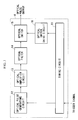
- Figure 1 is a diagram showing the structure of the optical pulse output circuit in an EOS oscilloscope in accordance with an embodiment of the present invention.
- Figure 2 is a diagram showing an example of a spectral analysis of the output of the optical filter.
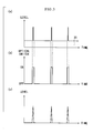
- Figure 3 is a diagram showing an example of the output of the optical filter and optical switch, and showing an example of the ON and OFF operation of the optical switch.
- Figure 4 is a diagram showing the structure of an optical pulse output circuit of an EOS oscilloscope in accordance with another embodiment of the present invention.
- Figure 5 is a diagram which serves to explain the measurement concept of the electro-optic probe in an EOS oscilloscope.
- Figure 6 is a diagram showing an example of the structure of an EOS oscilloscope.
- Figure 7 is a diagram showing an example of the structure of a conventional example of an optical pulse output circuit of an EOS oscilloscope.
- Figure 8 is a diagram showing an example of a spectral analysis of the output of the optical amplifier circuit in Figure 7.
- Figure 9 is a diagram showing an example of the output over time of the optical amplifier circuit in Figure 7.
- FIG. 6 shows an example of the structure of the EOS oscilloscope.
- the EOS oscilloscope comprises an EOS oscilloscope main body 1 and an electro-optic probe 2.
- An optical pulse supplied to the electro-optic probe 2 is generated by the optical pulse output circuit 4 on the basis of a trigger signal from a trigger circuit 3.
- the polarization detection and the like thereof are conducted by a polarization detecting optical system (not depicted in the figure) within electro-optic probe 2, and the signal thereof is inputted into EOS oscilloscope main body 1.
- the amplification and A/D conversion of the signal are conducted by A/D circuit 5, and processing for the display and the like of the signal which is the subject of measurement is conducted by processing circuit 6.
- the characteristic feature of the EOS oscilloscope of the present invention lies in the optical pulse output circuit 4 shown in Figure 6; the structure of this circuit will be explained with reference to the figures.
- FIG. 1 shows the structure of the optical pulse output circuit 4 of an EOS oscilloscope in accordance with an embodiment of the present invention.
- optical pulse output circuit 4 comprises: a timing circuit 11, which generates a timing signal which serves as the optical pulse generating timing based on the trigger signal; an optical pulse generating circuit 12, which conducts the generation of a sample optical pulse from the timing signal of timing signal 11; an optical amplifier circuit 13, which conducts the optical amplification of the sample optical pulse generated by optical pulse generating circuit 12; an optical filter 14, which blocks the propagation of the spontaneously emitted light from the optical amplifier circuit 13; an optical switch 15 which conducts the ON and OFF state of the light; and an optical switch drive circuit 16, which conducts the drive and control of the ON and OFF state of the optical switch 15 based on the timing signal from timing circuit 11.
- Timing circuit 11 generates a timing signal which serves as the optical pulse generating timing, based on a the trigger signal from the trigger circuit 3. This timing signal is supplied to the optical pulse generating circuit 12 and the optical switch drive circuit 16. A timing signal which serves to control the generation of the optical pulse at, for example, 30 [ps] at intervals of 250 [ns], is generated by this timing circuit 11.
- timing signal is so as to facilitate synchronization with the signal processing in the processing circuit 6 shown in Figure 6. It is desirable that the timing signal be generated based on the trigger signal; however, this is not necessarily so limited, and generation may be conducted using other clock signals.
- Optical pulse generating circuit 12 conducts the generation of a sample optical pulse using the timing signal of timing circuit 11.
- a laser diode for example, is employed as the optical pulse generating circuit 12, and optical pulses of a single wavelength, for example, 1.3 or 1.55 [micrometers], are generated.
- the amount of light of the sample optical pulse generated by optical pulse generating circuit 12 is insufficient for use as the optical pulse which is inputted into the electro-optic crystal 22 shown in Figure 5.
- the optical amplification of the sample optical pulse generated by optical pulse generating circuit 12 is conducted by optical amplifier circuit 13.
- FIG 8 An example of a spectral analysis of light outputted from this optical amplifier circuit 13 is shown in Figure 8; frequencies other than the frequency outputted from optical pulse generating circuit 12 are also generated and constitute noise.
- the light outputted from optical amplifier circuit 13 is inputted into optical filter 14.
- An example of a spectral analysis of the light outputted by optical filter 14 is shown in Figure 2. As can be seen from a comparison with Figure 8, by passing the light through this optical filter 14, it is possible to decrease the unnecessary light which does not contribute to the sampling in the spectra, and it is thus possible to increase measurement accuracy using this EOS oscilloscope.
- optical switch 15 and optical switch drive circuit 16 are provided, and by synchronization with the sample optical pulse, causing the optical switch 15 to transmit light when the sample optical pulse is being generated and isolating the optical switch 15 when the sample optical pulse is not being generated, the ON and OFF control is conducted, and the removal of this noise 31 is accomplished.
- optical switch drive circuit 16 generates a drive signal based on the timing from timing circuit 11 which causes optical switch 15 to transmit light when the sample optical pulse is being generated by optical pulse generating circuit 12, and which isolates the optical switch 15 when the sample optical pulse is not being generated by optical pulse generating circuit 12, and supplies this drive signal to optical switch 15.
- optical switch 15 enters an ON or OFF state with respect to the light passing through the optical switch 15 based on the drive signal from the optical switch drive circuit 10.
- an auditory optical switch AO switch
- E/O switch a entry wave path type optical switch
- optical switch 15 operated with a certain delay with respect to the drive signal. For this reason, the ON and OFF operation of the optical switch was not completely synchronized with the timing signal of timing circuit 11, but rather was delayed by a certain period of time. Furthermore, the duration of time of the timing signal for optical pulse generation which was produced by timing circuit 11 was on the order of few tens of ps, so that as a result of the delay in the ON and OFF operation of optical switch 15, some unnecessary light which did not contribute to the sampling on the time axis remained in the optical pulse which was outputted by optical pulse output circuit 4.
- the timing signals are sent to the optical pulse generating circuit 12 with allowance made for the delay in the ON and OFF operation of the optical switch 15.
- Figure 4 shows the structure of the optical pulse output circuit 4 in an EOS oscilloscope in accordance with the second embodiment of the present invention.
- parts which correspond to the parts shown in Figure 1 are given identical reference numbers, and an explanation thereof will be omitted here.
- a delay period correcting circuit 17 is provided which delays the timing signal generated by timing circuit 11 by the delay period of the optical switch 14, and outputs this delayed timing signal to the optical pulse generating circuit 12.
- this delay period correcting circuit 17 a timing signal which is delayed by the delay period of the operation of optical switch 15, in comparison with the timing signal sent to optical switch drive circuit 16, is sent to optical pulse generating circuit 12.
- the sample optical pulse produced by the optical pulse generating circuit 12 is synchronized with the ON and OFF operation of optical switch 15 and it thus becomes possible to conduct output of an optical pulse having no unnecessary light which does not contribute to the sampling on the time axis.
- the delay period correcting circuit 17 was provided within the timing circuit 11; however, this delay period correcting circuit 17 may be provided between the timing circuit 11 and the optical pulse generating circuit 12, and may have as the input signal thereof the timing signal generated by timing circuit 11, and may delay this inputted signal by an amount corresponding to the delay period of the operation of optical switch 15 to produce a timing signal, and may supply this timing signal to the optical pulse generating circuit 12.
- a memory may be provided within the delay period correcting circuit 17 in order to set the delay period so that the corrected delay period may be regulated.
- optical switch 14 shown in Figures 1 and 4 was provided between optical amplifier circuit 13 and optical switch 15; however, even if this is provided after optical switch 15, and the light outputted from optical switch 15 is inputted into optical filter 14, it is possible to achieve the same effects.
- an optical pulse output circuit which outputs an optical pulse for the purposes of observing the waveform of a signal to be measured
- the optical pulse output circuit has as the input light thereof a sample optical pulse amplified by an optical amplifier circuit, and outputs, as an optical pulse, the output from an optical filter which blocks the propagation of the spontaneously emitted light of the optical amplifier circuit.
- the optical pulse output circuit is provided with: a timing circuit which generates a timing signal which serves as the optical pulse generation timing, an optical pulse generating circuit which conducts the generation of a sample optical pulse on the basis of the timing signal of the timing circuit, an optical amplifier circuit which conducts the optical amplification of the sample optical pulse generated by the optical pulse generating circuit, and an optical filter which blocks the propagation of the spontaneously emitted light amplified by the optical amplifier circuit.
- an optical pulse output circuit which outputs an optical pulse for the purposes of observing the waveform of a signal to be measured
- the optical pulse output circuit controls the ON and OFF state of the sample optical pulse which was amplified by the optical amplifier circuit, and conducts the output of the optical pulse, using an optical switch synchronized with the sample optical pulse, by causing the optical switch to conduct light when the sample optical pulse is being generated, and cutting off the optical switch when the sample optical pulse is not being generated.
- the optical pulse output circuit is provided with: a timing circuit which generates a timing signal serving as the optical pulse generating timing, an optical pulse generating circuit, which conducts the generation of the sample optical pulse based on the timing signal from the timing circuit, an optical amplifier circuit, which conducts the optical amplification of the sample optical pulse generated by the optical pulse generating circuit, an optical switch which conducts the ON and OFF state of the light amplified by the optical amplifier circuit, and an optical switch drive circuit, which conducts the drive and control of the ON and OFF state of the optical switch based on the timing signal of the timing circuit.
- an optical pulse output circuit which outputs an optical pulse for the purposes of observing the waveform of a signal to be measured
- the optical pulse output circuit is provided with an optical filter which serves to block the propagation of spontaneously emitted light with respect to a sample optical pulse amplified by an optical amplifier circuit
- the optical pulse output circuit controls the ON and OFF state of the sample optical pulse amplified by the optical amplifier circuit, using an optical switch synchronized with the sample optical pulse, by causing the optical switch to transmit light when the sample optical pulse is being generated, and cutting off the optical switch when the sample optical pulse is not being generated, and the amplified sample optical pulse is passed through the optical filter and the optical switch, and is outputted as an optical pulse.
- the optical pulse output circuit is provided with: a timing circuit which generates a timing signal which serves as the optical pulse generating timing, an optical pulse generating circuit which conducts the generation of the sample optical pulse on the basis of the timing signal from the timing circuit, an optical amplifier circuit, which conducts the optical amplification of the sample optical pulse generated by the optical pulse generating circuit, an optical switch, which controls the ON and OFF state of the light amplified by the optical amplifier circuit, an optical switch drive circuit, which conducts the drive and control of the ON and OFF state of the optical switch based on the timing signal of the timing circuit, and an optical filter, which is provided between the optical amplifier circuit and the optical switch, or after the optical switch, and which blocks the propagation of spontaneously emitted light amplified by the optical amplifier circuit.
- the timing circuit is provided with a delay period correcting circuit which generates a timing signal in which the timing signal is delayed by an amount corresponding to the delay period of the operation of the optical switch, and the timing signal generated by this delay period correcting circuit is supplied to the optical pulse generating circuit.
- the optical pulse output circuit is provided with a delay period correcting circuit, provided between the timing circuit and the optical pulse generating circuit, and the delay period correcting circuit employs as the input signal thereof the timing signal generated by the timing circuit, and delays this input signal by an amount corresponding to the delay period of the operation of the optical switch, and generates a timing signal, and supplies this timing signal to the optical pulse generating circuit.
- the timing circuit employs a trigger signal as the input signal, and generates the timing signal based on this trigger signal.
Landscapes
- Physics & Mathematics (AREA)
- General Physics & Mathematics (AREA)
- Measurement Of Current Or Voltage (AREA)
- Tests Of Electronic Circuits (AREA)
Applications Claiming Priority (3)
| Application Number | Priority Date | Filing Date | Title |
|---|---|---|---|
| JP27315797 | 1997-10-06 | ||
| JP9273157A JPH11108961A (ja) | 1997-10-06 | 1997-10-06 | 電気光学サンプリングオシロスコープ |
| JP273157/97 | 1997-10-06 |
Publications (2)
| Publication Number | Publication Date |
|---|---|
| EP0908734A2 true EP0908734A2 (de) | 1999-04-14 |
| EP0908734A3 EP0908734A3 (de) | 1999-11-03 |
Family
ID=17523910
Family Applications (1)
| Application Number | Title | Priority Date | Filing Date |
|---|---|---|---|
| EP98308133A Withdrawn EP0908734A3 (de) | 1997-10-06 | 1998-10-06 | Elektrooptisches Sampling-Oszilloskop |
Country Status (3)
| Country | Link |
|---|---|
| US (1) | US6252387B1 (de) |
| EP (1) | EP0908734A3 (de) |
| JP (1) | JPH11108961A (de) |
Families Citing this family (1)
| Publication number | Priority date | Publication date | Assignee | Title |
|---|---|---|---|---|
| JP4970640B2 (ja) * | 2000-05-19 | 2012-07-11 | ルネサスエレクトロニクス株式会社 | スクリーニング方法、スクリーニング装置及び記録媒体 |
Family Cites Families (1)
| Publication number | Priority date | Publication date | Assignee | Title |
|---|---|---|---|---|
| EP0197196A1 (de) * | 1985-03-08 | 1986-10-15 | The University Of Rochester | Elektro-elektronenoptisches Oszilloskop zur Zeitauflösung elektrischer Wellenzüge im Picosekundenbereich |
-
1997
- 1997-10-06 JP JP9273157A patent/JPH11108961A/ja active Pending
-
1998
- 1998-10-06 US US09/167,234 patent/US6252387B1/en not_active Expired - Fee Related
- 1998-10-06 EP EP98308133A patent/EP0908734A3/de not_active Withdrawn
Also Published As
| Publication number | Publication date |
|---|---|
| JPH11108961A (ja) | 1999-04-23 |
| EP0908734A3 (de) | 1999-11-03 |
| US6252387B1 (en) | 2001-06-26 |
Similar Documents
| Publication | Publication Date | Title |
|---|---|---|
| EP0294836B1 (de) | Spannungsdetektor | |
| KR100401347B1 (ko) | 광구동형 드라이버, 광출력형 전압센서 및 이들을 이용한ic시험장치 | |
| US5189483A (en) | Apparatus for measurement of chromatic dispersion in a single mode optical fiber | |
| US4982151A (en) | Voltage measuring apparatus | |
| US5319266A (en) | Differential boxcar integrator with auto-zero function | |
| US6252387B1 (en) | Oscilloscope utilizing probe with electro-optic crystal | |
| US6912046B2 (en) | Instrument measuring chromatic dispersion in optical fibers | |
| EP0943925A3 (de) | Elektro-optisches Abtast-Oszilloskop | |
| JPH0512657B2 (de) | ||
| US4219762A (en) | Wideband self-calibrated fiber-optic data link with fiber-optic storage | |
| US6297651B1 (en) | Electro-optic sampling probe having unit for adjusting quantity of light incident on electro-optic sampling optical system module | |
| US6507014B2 (en) | Electro-optic probe | |
| EP0212804A2 (de) | Messsystem für optische Fasern mit vielfacher Wellenlänge | |
| Aoshima et al. | Improvement of the minimum detectability of electro-optic sampling by using a structurally new probe | |
| JP3372491B2 (ja) | 電気光学サンプリングオシロスコープ及び電気光学サンプリングオシロスコープ用プローブ | |
| Priyadarshi et al. | In-situ electro-optic sampling of microwave signals applied to superconducting circuits | |
| WO2002016901A2 (en) | Instrument measuring chromatic dispersion in optical fibers | |
| JP2000162243A (ja) | 電気光学サンプリングプローバ | |
| JP2972973B2 (ja) | 光パルス試験器 | |
| US6377036B1 (en) | Electro-optic sampling oscilloscope | |
| JP2000221213A (ja) | 電気光学プロ―ブ | |
| GB2346692A (en) | Electro-optic probe | |
| JPH0574013B2 (de) | ||
| JPH0862051A (ja) | 繰り返し光波形生成装置 | |
| JP2002022600A (ja) | 光線路試験装置および光線路試験方法 |
Legal Events
| Date | Code | Title | Description |
|---|---|---|---|
| PUAI | Public reference made under article 153(3) epc to a published international application that has entered the european phase |
Free format text: ORIGINAL CODE: 0009012 |
|
| AK | Designated contracting states |
Kind code of ref document: A2 Designated state(s): DE FR GB |
|
| AX | Request for extension of the european patent |
Free format text: AL;LT;LV;MK;RO;SI |
|
| PUAL | Search report despatched |
Free format text: ORIGINAL CODE: 0009013 |
|
| AK | Designated contracting states |
Kind code of ref document: A3 Designated state(s): AT BE CH CY DE DK ES FI FR GB GR IE IT LI LU MC NL PT SE |
|
| AX | Request for extension of the european patent |
Free format text: AL;LT;LV;MK;RO;SI |
|
| RIC1 | Information provided on ipc code assigned before grant |
Free format text: 6G 01R 13/34 A, 6G 01R 1/07 B |
|
| 17P | Request for examination filed |
Effective date: 20000210 |
|
| AKX | Designation fees paid |
Free format text: DE FR GB |
|
| 17Q | First examination report despatched |
Effective date: 20050216 |
|
| RAP1 | Party data changed (applicant data changed or rights of an application transferred) |
Owner name: NIPPON TELEGRAPH ANDTELEPHONE CORPORATION Owner name: YOKOGAWA ELECTRIC CORPORATION |
|
| GRAP | Despatch of communication of intention to grant a patent |
Free format text: ORIGINAL CODE: EPIDOSNIGR1 |
|
| STAA | Information on the status of an ep patent application or granted ep patent |
Free format text: STATUS: THE APPLICATION IS DEEMED TO BE WITHDRAWN |
|
| 18D | Application deemed to be withdrawn |
Effective date: 20060321 |