EP0908865A1 - Dispositif d'affichage - Google Patents
Dispositif d'affichage Download PDFInfo
- Publication number
- EP0908865A1 EP0908865A1 EP98810987A EP98810987A EP0908865A1 EP 0908865 A1 EP0908865 A1 EP 0908865A1 EP 98810987 A EP98810987 A EP 98810987A EP 98810987 A EP98810987 A EP 98810987A EP 0908865 A1 EP0908865 A1 EP 0908865A1
- Authority
- EP
- European Patent Office
- Prior art keywords
- base plate
- display
- display device
- electrode
- display unit
- Prior art date
- Legal status (The legal status is an assumption and is not a legal conclusion. Google has not performed a legal analysis and makes no representation as to the accuracy of the status listed.)
- Granted
Links
- 239000004020 conductor Substances 0.000 claims abstract description 10
- 239000000969 carrier Substances 0.000 claims abstract description 4
- 239000000463 material Substances 0.000 claims description 6
- 230000000694 effects Effects 0.000 claims description 3
- 239000012777 electrically insulating material Substances 0.000 claims 1
- 230000008020 evaporation Effects 0.000 description 1
- 238000001704 evaporation Methods 0.000 description 1
- PCHJSUWPFVWCPO-UHFFFAOYSA-N gold Chemical compound [Au] PCHJSUWPFVWCPO-UHFFFAOYSA-N 0.000 description 1
- 239000010931 gold Substances 0.000 description 1
- 229910052737 gold Inorganic materials 0.000 description 1
- 239000011810 insulating material Substances 0.000 description 1
- 238000004020 luminiscence type Methods 0.000 description 1
- 239000002184 metal Substances 0.000 description 1
- 229910052751 metal Inorganic materials 0.000 description 1
- 230000001681 protective effect Effects 0.000 description 1
- 125000006850 spacer group Chemical group 0.000 description 1
- 239000012780 transparent material Substances 0.000 description 1
Images



Classifications
-
- G—PHYSICS
- G09—EDUCATION; CRYPTOGRAPHY; DISPLAY; ADVERTISING; SEALS
- G09F—DISPLAYING; ADVERTISING; SIGNS; LABELS OR NAME-PLATES; SEALS
- G09F9/00—Indicating arrangements for variable information in which the information is built-up on a support by selection or combination of individual elements
- G09F9/30—Indicating arrangements for variable information in which the information is built-up on a support by selection or combination of individual elements in which the desired character or characters are formed by combining individual elements
- G09F9/37—Indicating arrangements for variable information in which the information is built-up on a support by selection or combination of individual elements in which the desired character or characters are formed by combining individual elements being movable elements
- G09F9/375—Indicating arrangements for variable information in which the information is built-up on a support by selection or combination of individual elements in which the desired character or characters are formed by combining individual elements being movable elements the position of the elements being controlled by the application of a magnetic field
Definitions
- the present invention relates to a display device Display units which point the image to be reproduced represent, the respective display unit a display dot and means for actuating this display dot.
- the dot of the each display unit has a base plate.
- the one another opposite large areas of this base plate a large color contrast.
- One of the large areas of the Base plate is black, while the other large area e.g. is yellow.
- the base plate carries a permanent magnet.
- the Display unit further includes a controllable magnetic Circle with an approximately U-shaped yoke.
- the dot plate is the Poles assigned to this yoke, which together with the permanent magnet an adjustment of the display dot enables.
- This display device further comprises a light source, which precedes the dots of the display units and which ones is in permanent operation when required. If nothing appears then the black side of all display dots is the Opposite viewer.
- Those display units are used to display an image driven, which is based on the representation of the Image should participate. With these, the display dot is reversed so that the viewer faces his yellow page. The yellow surface of the display dot reflects the light from the Light source to the viewer.
- This known display device must be towards the viewer be arranged so that the display units preceding light source does not blind the viewer.
- the Display units usually form horizontal and rows on top of each other.
- the light source is mostly below of the panel from the display units and in a specific one Distance arranged in front of this. In this case, appear the display dots of the bottom rows are lighter than the display dots the top rows, which is the result of reading the such device to convey information unfavorably affects. Because of the light source and because of the need for it To arrange at a distance in front of the display panel, such Indicators have considerable dimensions, which do not let the display shrink in this system.
- the object of the present invention is the mentioned as well to eliminate still further disadvantages of the prior art.
- the present display device has display units 1 on, of which only a single side view in Fig. 1 is shown. Such display units 1 are used point by point representation of the image to be reproduced and them in the present device form rows which are parallel run to each other and which are carried by a plate 2 are. In the present case can also on the support plate 2 Conductor tracks 41, 42, 43 and 44 and components (not shown) be attached, which for the electrical connection and operation of the display units 1 are required.
- the present Setup also includes a see-through front panel 3, which the display units 1 as protection against unwanted mechanical effects is preceded. This The protective plate 3 is on the support plate 2 via spacers 4 attached.
- the respective display unit 1 comprises a display dot 10 as well Means for actuating this display dot 10.
- the mode of operation this display dot 10 makes the electroluminescent effect advantage.
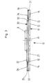
- the display dot 10 has a base plate 11 , which are provided with an electroluminescent device 30 is.
- This electroluminescent device 30 can, for example be an electroluminescent lamp.
- 2 to 5 the display dot 10 is shown in that end position in which he is out of service or inactive.
- the base plate 11 is in the present case from an electrically insulating and transparent or at least translucent material.
- the base plate 11 has in the case shown (Fig. 2 and 3) an essentially octagonal floor plan. From two each other opposite sides 12 and 13 of the base plate 11 are one rag each. Foothills 14 and 15, which on a common axis A lie. This axis A also represents the Rotation or pivot axis of the display dot 10 represents another two mutually parallel sides 16 and 17 are in the substantially perpendicular to said pages 12 and 13 of the Base plate 11. The edge of one of these sides 16 has in the illustrated Fall in a straight line. In the other side 17, however, is a recess 17 with an arcuate Contour executed. The purpose of this recess 17 is from the The following can be seen. Pages 18, 19, 20 and 21 the base plate 11, which said pairs of sides 12th and 13 and 16 and 17 connect with each other, run in illustrated case straight, although it is also another Can have a course.
- This EL device 30 includes a first electrode 31, which also can be referred to as a front electrode and which also is transparent or at least translucent. Such electrodes are generally known and can, for example, by Evaporation of metal can be produced on the base plate 11.
- This front electrode 31 adheres firmly to the base plate 11 and it covers practically the entire surface of the base plate 11. It extends into the area of one of the lobes 15 on the base plate 11, the surface of this electrode 31 also covered. Ends in the area of the other flap 14 this front electrode 31 at a distance from it.
- the EL device 30 further includes a second one Electrode 32, which in the following also serves as a back electrode referred to as. This electrode 32 covers practically the whole Back of the EL layer 33 and it extends up to the area of the other tab 14 on the base plate 11, the Surface also covers them.
- contact pieces 35 and 36 (FIGS. 2 to 6) made of an electrical conductive material provided, one each that section of the respective electrode 31 or 32 electrically is conductively attached, which is in the area of one of the lobes 14 or 15 is located.
- the respective contact piece 35 or 36 has practically the shape of a cuboid, which over one of its Large or side surfaces on the tab 14 or 15 attached is.
- the opposite or parallel basic or Side surface of this cuboid 35 or 36 is with a contact layer 34, for example made of gold.
- the width of the cuboid 35 or 36 is smaller than the width of this load-bearing flap 14 and 15.
- the contact pieces 35 and 36 on tabs 14 and 15 with respect to the pivot axis A arranged asymmetrically.
- the display unit 1 is also designed so that the EL device 30 optionally or controllable to a source of electrical Energy (not shown) can be connected.
- the base plate 11 of the display dot 10 pivotally mounted.
- the display unit 1 comprises two rod-shaped carriers 22, which on opposite sides 12 and 13 of the Base plate 11 are arranged and of which in Fig. 1 only the front carrier 22 can be seen. These carriers 22 are attached at one end in the support plate 2, of which they are practical protrude at right angles.
- the in the area of the support plate 2 lying ends of the carrier 22 are on those conductor tracks 41 and 42 connected to the support plate 2, which to the above Lead supply source for the EL device 30.
- a bearing sleeve 23 or 24 attached at the free end of the respective carrier 22 .
- Both the carrier 22 and the bearing sleeves 23 and 24 are made of an electrically conductive material. Consequently, the bearing sleeves 23 and 24 via the carrier 22 and the mentioned conductor tracks 41 and 42 on the support plate 2 the power source connected.
- the one facing away from rag 14 or 15 Large or side surface of the cuboid contact piece 35 and 36 can be convex, the curvature of these Area of curvature of the inner wall of the bearing sleeve 23 or 24 can correspond.
- the display unit 1 further comprises a controllable magnetic Circle 25.
- This magnetic circuit 25 essentially contains one U-shaped yoke 26 with legs 27 and 28 and with a web 29 connecting these.
- the yoke 26 is with a Provide coil 9, which in the case shown on the web 29th is appropriate.
- This coil 9 is on conductor tracks 43 and 44 the support plate 2 connected (not shown), via which the commands necessary for the function of the display unit 1 can receive.
- the yoke 26 is arranged such that the legs 27 and 28 the same are practically perpendicular to the support plate 2 and that they are in a vertical plane.
- the sleeve carrier 22 are also in a vertical plane. These two vertical ones Layers are practically perpendicular to each other.
- the yoke 26 is also arranged so that at least the end parts of it Legs 27 and 28 protrude from the same side of the support plate 2 as the carrier 22. The distance between the bearing sleeves 14th and 15 and the end surfaces 37 and 38 of the yoke legs 27 and 28 from the support plate 2 practically the same size.
- One of the extensions is in the respective bearing sleeve 23 or 24 or rag 14 or 15 of the base plate 11 pivotally mounted.
- the width of the flap 14 or 15 is so much smaller than the inner diameter of the bearing sleeve 23 or 24 that the rag is even stored with play in the sleeve.
- the base plate mounted in the sleeves 23 and 24 11 also includes the end surfaces 37 and 38 Assigned sections of the yoke legs 27 and 28. Since the vertical planes of the supports 22 and the yoke legs 27 and 28 are perpendicular to each other, the end surfaces are 37 and 38 the yoke legs 27 and 28 perpendicular to the above standing short sides 16 and 17 of the base plate 11 assigned.
- the display dot 10 is with a rod-shaped permanent magnet 8 provided, which on the outside of the back electrode 32nd the EL device 30 is attached.
- the rod 8 is arranged that its longitudinal axis is perpendicular to the pivot axis A. and that the poles N and S of the magnet 8 thus the yoke legs 27 and 28 are facing.
- a well-known cooperation of the magnetic circuit 25 with the permanent magnet 8 causes an adjustment of the base plate 11 and thus also of the entire display dot 10 from one of the end positions of the Display dots 10 in its other end position and back.
- the distance between the yoke legs 27 and 28 is as follows set.
- A comprising the first vertical short side 16
- Edge of the base plate 11 lies on the end or End face 37 of one of the yoke legs 27.
- This is one of the End positions which the base plate 11 can assume.
- This End position is shown in Fig. 2 and the display dot 10 inactive in this end position.
- the above or outside large area of the base plate 11 is with the EL device 30 provided. In this case, however, the back electrode is located 32 above or on the outside of the EL device 30.
- the other yoke leg 28 lies in this first end position in the recess 17 in the base plate 11, which partially surrounds this yoke leg 28. This reduces the magnetic resistance of the gap between this yoke leg 28 and the base plate 11.
- the base plate 11 When the display unit 1 is actuated, the base plate 11 their other end position. Here comes the short vertical Page 16 of the base body 11 on the end face 38 of the other Yoke leg 28 for the edition. The angle of the swivel movement the base plate 11 is almost 180 degrees, so that opposite large area of the base plate 11 in the illustrated Case comes up. This second large area of the base plate 11 is free and because it is made of a transparent material is the front electrode 31 of the EL device 30 through the Base plate 11 now visible.
- FIG. 5 shows a side view of one of the tabs 15 on Base body 11 of the display dot 10 when it is in a its end positions.
- the base plate 11 and thus in this case also the flap 15 is at the bottom and Display dot 10 is thus over the tab 15 on the bearing sleeve 24 on. Since the base body 11 and the tab 15 from an electrical insulating material, there can be no current between the electrically conductive bearing sleeve 24 and the front electrode 31 of the display dot 10 flow.
- the display dot is in this case inactive, what the same position shown in Figs. 1 and 2 corresponds.
- Fig. 6 shows a side view of the other end position of the Display dots 10.
- the base plate 11 is almost in this case Swiveled 180 degrees so that the contact piece 36 is now located below and the contact layer attached to its top 34 lies directly on the conductive bearing sleeve 24 on.
- current can flow through the contact layer 34 and the contact piece 36 between the bearing sleeve 24 and the front electrode 31 flow.
- the same situation exists in this case with the opposite bearing sleeve 23, where Current between this and the back electrode 32 via the contact layer 34 and the contact piece 36 can flow.
- the current can in this case through the layer 33 of the electroluminescent material flow and light is emitted by this EL device 30 radiated through the base plate 11.
Landscapes
- Physics & Mathematics (AREA)
- General Physics & Mathematics (AREA)
- Engineering & Computer Science (AREA)
- Theoretical Computer Science (AREA)
- Devices For Indicating Variable Information By Combining Individual Elements (AREA)
- Electroluminescent Light Sources (AREA)
- Illuminated Signs And Luminous Advertising (AREA)
Applications Claiming Priority (3)
| Application Number | Priority Date | Filing Date | Title |
|---|---|---|---|
| CH02342/97A CH692682A5 (de) | 1997-10-06 | 1997-10-06 | Anzeigeeinrichtung. |
| CH2342/97 | 1997-10-06 | ||
| CH234297 | 1997-10-06 |
Publications (2)
| Publication Number | Publication Date |
|---|---|
| EP0908865A1 true EP0908865A1 (fr) | 1999-04-14 |
| EP0908865B1 EP0908865B1 (fr) | 2002-12-11 |
Family
ID=4231572
Family Applications (1)
| Application Number | Title | Priority Date | Filing Date |
|---|---|---|---|
| EP98810987A Expired - Lifetime EP0908865B1 (fr) | 1997-10-06 | 1998-10-01 | Dispositif d'affichage |
Country Status (6)
| Country | Link |
|---|---|
| US (1) | US6229517B1 (fr) |
| EP (1) | EP0908865B1 (fr) |
| AT (1) | ATE229680T1 (fr) |
| CA (1) | CA2249491A1 (fr) |
| CH (1) | CH692682A5 (fr) |
| DE (1) | DE59806613D1 (fr) |
Families Citing this family (4)
| Publication number | Priority date | Publication date | Assignee | Title |
|---|---|---|---|---|
| WO2003037039A1 (fr) * | 2001-10-24 | 2003-05-01 | Lumitec Ag | Affichage electroluminescent tridimensionnel |
| EP2069892B1 (fr) * | 2006-09-27 | 2013-03-13 | Bandit Inc. | Affichage magnétique pour montres |
| US8279935B2 (en) * | 2007-09-27 | 2012-10-02 | Intel Corporation | Method and apparatus for image quality control in video data |
| US20110158057A1 (en) * | 2009-04-02 | 2011-06-30 | Brewer Donald R | Magnetic display for watches |
Citations (4)
| Publication number | Priority date | Publication date | Assignee | Title |
|---|---|---|---|---|
| FR2543336A2 (fr) * | 1981-05-05 | 1984-09-28 | Nec | Dispositif d'affichage alphanumerique |
| US4531318A (en) * | 1983-09-16 | 1985-07-30 | Nei Canada Limited | Display or indicating element with bent core |
| WO1987006047A1 (fr) * | 1986-03-25 | 1987-10-08 | Dol Honore | Dispositif electronique de visualisation et d'affichage integral |
| EP0291122A1 (fr) * | 1987-05-13 | 1988-11-17 | Koninklijke Philips Electronics N.V. | Dispositif d'affichage électroscopique |
Family Cites Families (4)
| Publication number | Priority date | Publication date | Assignee | Title |
|---|---|---|---|---|
| US4074253A (en) * | 1975-11-19 | 1978-02-14 | Kenneth E. Macklin | Novel bistable light modulators and display element and arrays therefrom |
| US4794391A (en) * | 1983-10-31 | 1988-12-27 | Securite Et Signalisation | Display matrix incorporating light-conducting fibers and light-occulting shutters |
| US5898418A (en) * | 1995-03-06 | 1999-04-27 | Kao; Pin-Chi | Magnetically operated display |
| JP3899566B2 (ja) * | 1996-11-25 | 2007-03-28 | セイコーエプソン株式会社 | 有機el表示装置の製造方法 |
-
1997
- 1997-10-06 CH CH02342/97A patent/CH692682A5/de not_active IP Right Cessation
-
1998
- 1998-10-01 AT AT98810987T patent/ATE229680T1/de not_active IP Right Cessation
- 1998-10-01 EP EP98810987A patent/EP0908865B1/fr not_active Expired - Lifetime
- 1998-10-01 DE DE59806613T patent/DE59806613D1/de not_active Expired - Fee Related
- 1998-10-05 US US09/166,085 patent/US6229517B1/en not_active Expired - Fee Related
- 1998-10-05 CA CA002249491A patent/CA2249491A1/fr not_active Abandoned
Patent Citations (4)
| Publication number | Priority date | Publication date | Assignee | Title |
|---|---|---|---|---|
| FR2543336A2 (fr) * | 1981-05-05 | 1984-09-28 | Nec | Dispositif d'affichage alphanumerique |
| US4531318A (en) * | 1983-09-16 | 1985-07-30 | Nei Canada Limited | Display or indicating element with bent core |
| WO1987006047A1 (fr) * | 1986-03-25 | 1987-10-08 | Dol Honore | Dispositif electronique de visualisation et d'affichage integral |
| EP0291122A1 (fr) * | 1987-05-13 | 1988-11-17 | Koninklijke Philips Electronics N.V. | Dispositif d'affichage électroscopique |
Also Published As
| Publication number | Publication date |
|---|---|
| US6229517B1 (en) | 2001-05-08 |
| CH692682A5 (de) | 2002-09-13 |
| CA2249491A1 (fr) | 1999-04-06 |
| DE59806613D1 (de) | 2003-01-23 |
| ATE229680T1 (de) | 2002-12-15 |
| EP0908865B1 (fr) | 2002-12-11 |
Similar Documents
| Publication | Publication Date | Title |
|---|---|---|
| DE68917694T2 (de) | Schaltungsplattenzusammenbau und Kontaktstift, der darin verwendet wird. | |
| DE2715660C3 (de) | Verfahren zum Verbinden der Einführungsdrähte von Blitzlampen einer Vielfach-Blitzlampenanordnung | |
| DE102006059509B4 (de) | Organisches Leuchtbauelement | |
| EP0937305B2 (fr) | Systeme de commutateur selon la technique mid | |
| DE1949966A1 (de) | UEber Nocken betaetigbarer Schalter mit beweglichen und festen Kontakten,insbesondere fuer gedruckte Leiterplatten | |
| DE102015117486A1 (de) | Organische Leuchtdiode und Anordnung mit einer organischen Leuchtdiode | |
| EP3819999A1 (fr) | Connecteur enfichable à encastrer | |
| DE2825284C3 (de) | Blitzlampenanordnung | |
| DE69800386T2 (de) | Tafel zum Montieren von Anzeigeelementen | |
| DE2721166C3 (de) | Blitzlampenanordnung | |
| DE3608617A1 (de) | Anzeigegeraet | |
| EP0908865B1 (fr) | Dispositif d'affichage | |
| EP1323807A2 (fr) | Dispositif d'éclairage électroluminescent | |
| DE19619814C2 (de) | Anzeigeeinrichtung | |
| DE29900384U1 (de) | Schmückende Beleuchtungsvorrichtung mit einem flexibel formbaren Lichtemissionsschlauch, wodurch vom Benutzer konzipierte Zeichen blinkend anzeigbar sind | |
| DE3146247A1 (de) | Bauelement | |
| DE2841922C3 (de) | Vielfach-Blitzlampenanordnung | |
| DE2703996A1 (de) | Vielfach-blitzlampenanordnung mit einem leitfaehigen reflektor | |
| DE8712960U1 (de) | Lichtdurchlässiges Kunststoff-Folienteil zum Schutz von Anzeigeelementen | |
| DE2835901C3 (de) | Blitzlampenanordnung | |
| DE3412430C2 (fr) | ||
| DE9200772U1 (de) | Näherungsschalter mit Schaltzustandsanzeige | |
| DE3601941C2 (fr) | ||
| DE19802269A1 (de) | Elektrolumineszenzelement und Verfahren zu dessen Herstellung | |
| DE2542114C3 (de) | Vielfach-Blitzlampenanordnung |
Legal Events
| Date | Code | Title | Description |
|---|---|---|---|
| PUAI | Public reference made under article 153(3) epc to a published international application that has entered the european phase |
Free format text: ORIGINAL CODE: 0009012 |
|
| AK | Designated contracting states |
Kind code of ref document: A1 Designated state(s): AT CH DE FR GB IT LI |
|
| AX | Request for extension of the european patent |
Free format text: AL;LT;LV;MK;RO;SI |
|
| AKX | Designation fees paid | ||
| 17P | Request for examination filed |
Effective date: 19991221 |
|
| RBV | Designated contracting states (corrected) |
Designated state(s): AT CH DE FR GB IT LI |
|
| 17Q | First examination report despatched |
Effective date: 20001110 |
|
| GRAG | Despatch of communication of intention to grant |
Free format text: ORIGINAL CODE: EPIDOS AGRA |
|
| GRAG | Despatch of communication of intention to grant |
Free format text: ORIGINAL CODE: EPIDOS AGRA |
|
| GRAH | Despatch of communication of intention to grant a patent |
Free format text: ORIGINAL CODE: EPIDOS IGRA |
|
| GRAH | Despatch of communication of intention to grant a patent |
Free format text: ORIGINAL CODE: EPIDOS IGRA |
|
| GRAA | (expected) grant |
Free format text: ORIGINAL CODE: 0009210 |
|
| AK | Designated contracting states |
Kind code of ref document: B1 Designated state(s): AT CH DE FR GB IT LI |
|
| PG25 | Lapsed in a contracting state [announced via postgrant information from national office to epo] |
Ref country code: IT Free format text: LAPSE BECAUSE OF FAILURE TO SUBMIT A TRANSLATION OF THE DESCRIPTION OR TO PAY THE FEE WITHIN THE PRESCRIBED TIME-LIMIT;WARNING: LAPSES OF ITALIAN PATENTS WITH EFFECTIVE DATE BEFORE 2007 MAY HAVE OCCURRED AT ANY TIME BEFORE 2007. THE CORRECT EFFECTIVE DATE MAY BE DIFFERENT FROM THE ONE RECORDED. Effective date: 20021211 Ref country code: GB Free format text: LAPSE BECAUSE OF FAILURE TO SUBMIT A TRANSLATION OF THE DESCRIPTION OR TO PAY THE FEE WITHIN THE PRESCRIBED TIME-LIMIT Effective date: 20021211 Ref country code: FR Free format text: LAPSE BECAUSE OF NON-PAYMENT OF DUE FEES Effective date: 20021211 |
|
| REF | Corresponds to: |
Ref document number: 229680 Country of ref document: AT Date of ref document: 20021215 Kind code of ref document: T |
|
| REG | Reference to a national code |
Ref country code: GB Ref legal event code: FG4D Free format text: NOT ENGLISH |
|
| REG | Reference to a national code |
Ref country code: CH Ref legal event code: EP |
|
| REF | Corresponds to: |
Ref document number: 59806613 Country of ref document: DE Date of ref document: 20030123 |
|
| REG | Reference to a national code |
Ref country code: CH Ref legal event code: NV Representative=s name: PATENTANWALTSBUERO DIPL.-ING. S. V. KULHAVY + CO. |
|
| GBV | Gb: ep patent (uk) treated as always having been void in accordance with gb section 77(7)/1977 [no translation filed] |
Effective date: 20021211 |
|
| PLBE | No opposition filed within time limit |
Free format text: ORIGINAL CODE: 0009261 |
|
| STAA | Information on the status of an ep patent application or granted ep patent |
Free format text: STATUS: NO OPPOSITION FILED WITHIN TIME LIMIT |
|
| EN | Fr: translation not filed | ||
| 26N | No opposition filed |
Effective date: 20030912 |
|
| PGFP | Annual fee paid to national office [announced via postgrant information from national office to epo] |
Ref country code: AT Payment date: 20051031 Year of fee payment: 8 |
|
| PGFP | Annual fee paid to national office [announced via postgrant information from national office to epo] |
Ref country code: DE Payment date: 20051221 Year of fee payment: 8 |
|
| PGFP | Annual fee paid to national office [announced via postgrant information from national office to epo] |
Ref country code: CH Payment date: 20060120 Year of fee payment: 8 |
|
| PG25 | Lapsed in a contracting state [announced via postgrant information from national office to epo] |
Ref country code: AT Free format text: LAPSE BECAUSE OF NON-PAYMENT OF DUE FEES Effective date: 20061001 |
|
| PG25 | Lapsed in a contracting state [announced via postgrant information from national office to epo] |
Ref country code: LI Free format text: LAPSE BECAUSE OF NON-PAYMENT OF DUE FEES Effective date: 20061031 Ref country code: CH Free format text: LAPSE BECAUSE OF NON-PAYMENT OF DUE FEES Effective date: 20061031 |
|
| PG25 | Lapsed in a contracting state [announced via postgrant information from national office to epo] |
Ref country code: DE Free format text: LAPSE BECAUSE OF NON-PAYMENT OF DUE FEES Effective date: 20070501 |
|
| REG | Reference to a national code |
Ref country code: CH Ref legal event code: PL |