EP0908958B1 - Diffusion in-situ de dopant durant la croissance en réseau dendritique d'un ruban cristal de silicium - Google Patents
Diffusion in-situ de dopant durant la croissance en réseau dendritique d'un ruban cristal de silicium Download PDFInfo
- Publication number
- EP0908958B1 EP0908958B1 EP97117465A EP97117465A EP0908958B1 EP 0908958 B1 EP0908958 B1 EP 0908958B1 EP 97117465 A EP97117465 A EP 97117465A EP 97117465 A EP97117465 A EP 97117465A EP 0908958 B1 EP0908958 B1 EP 0908958B1
- Authority
- EP
- European Patent Office
- Prior art keywords
- dopant material
- web
- furnace
- heating
- solid
- Prior art date
- Legal status (The legal status is an assumption and is not a legal conclusion. Google has not performed a legal analysis and makes no representation as to the accuracy of the status listed.)
- Expired - Lifetime
Links
- 239000002019 doping agent Substances 0.000 title claims description 52
- 238000009792 diffusion process Methods 0.000 title claims description 46
- 239000013078 crystal Substances 0.000 title claims description 19
- XUIMIQQOPSSXEZ-UHFFFAOYSA-N Silicon Chemical compound [Si] XUIMIQQOPSSXEZ-UHFFFAOYSA-N 0.000 title claims description 12
- 229910052710 silicon Inorganic materials 0.000 title claims description 12
- 239000010703 silicon Substances 0.000 title claims description 12
- 238000011065 in-situ storage Methods 0.000 title description 5
- 239000012535 impurity Substances 0.000 title description 4
- 239000000463 material Substances 0.000 claims description 45
- 239000007787 solid Substances 0.000 claims description 40
- 238000010438 heat treatment Methods 0.000 claims description 21
- 238000000034 method Methods 0.000 claims description 18
- 239000000155 melt Substances 0.000 claims description 7
- 239000000289 melt material Substances 0.000 claims description 6
- 238000004519 manufacturing process Methods 0.000 claims description 5
- 210000001787 dendrite Anatomy 0.000 claims 2
- 238000000926 separation method Methods 0.000 description 3
- OKTJSMMVPCPJKN-UHFFFAOYSA-N Carbon Chemical compound [C] OKTJSMMVPCPJKN-UHFFFAOYSA-N 0.000 description 2
- 230000015572 biosynthetic process Effects 0.000 description 2
- 230000000694 effects Effects 0.000 description 2
- 229910002804 graphite Inorganic materials 0.000 description 2
- 239000010439 graphite Substances 0.000 description 2
- 238000009434 installation Methods 0.000 description 2
- 150000002500 ions Chemical class 0.000 description 2
- 239000004065 semiconductor Substances 0.000 description 2
- 239000000758 substrate Substances 0.000 description 2
- ZOXJGFHDIHLPTG-UHFFFAOYSA-N Boron Chemical compound [B] ZOXJGFHDIHLPTG-UHFFFAOYSA-N 0.000 description 1
- OAICVXFJPJFONN-UHFFFAOYSA-N Phosphorus Chemical compound [P] OAICVXFJPJFONN-UHFFFAOYSA-N 0.000 description 1
- 229910052796 boron Inorganic materials 0.000 description 1
- 238000005516 engineering process Methods 0.000 description 1
- 239000007788 liquid Substances 0.000 description 1
- 229910052698 phosphorus Inorganic materials 0.000 description 1
- 239000011574 phosphorus Substances 0.000 description 1
- 238000011112 process operation Methods 0.000 description 1
Images


Classifications
-
- H—ELECTRICITY
- H10—SEMICONDUCTOR DEVICES; ELECTRIC SOLID-STATE DEVICES NOT OTHERWISE PROVIDED FOR
- H10F—INORGANIC SEMICONDUCTOR DEVICES SENSITIVE TO INFRARED RADIATION, LIGHT, ELECTROMAGNETIC RADIATION OF SHORTER WAVELENGTH OR CORPUSCULAR RADIATION
- H10F77/00—Constructional details of devices covered by this subclass
- H10F77/10—Semiconductor bodies
- H10F77/12—Active materials
- H10F77/122—Active materials comprising only Group IV materials
- H10F77/1223—Active materials comprising only Group IV materials characterised by the dopants
-
- C—CHEMISTRY; METALLURGY
- C30—CRYSTAL GROWTH
- C30B—SINGLE-CRYSTAL GROWTH; UNIDIRECTIONAL SOLIDIFICATION OF EUTECTIC MATERIAL OR UNIDIRECTIONAL DEMIXING OF EUTECTOID MATERIAL; REFINING BY ZONE-MELTING OF MATERIAL; PRODUCTION OF A HOMOGENEOUS POLYCRYSTALLINE MATERIAL WITH DEFINED STRUCTURE; SINGLE CRYSTALS OR HOMOGENEOUS POLYCRYSTALLINE MATERIAL WITH DEFINED STRUCTURE; AFTER-TREATMENT OF SINGLE CRYSTALS OR A HOMOGENEOUS POLYCRYSTALLINE MATERIAL WITH DEFINED STRUCTURE; APPARATUS THEREFOR
- C30B15/00—Single-crystal growth by pulling from a melt, e.g. Czochralski method
- C30B15/02—Single-crystal growth by pulling from a melt, e.g. Czochralski method adding crystallising materials or reactants forming it in situ to the melt
- C30B15/04—Single-crystal growth by pulling from a melt, e.g. Czochralski method adding crystallising materials or reactants forming it in situ to the melt adding doping materials, e.g. for n-p-junction
-
- C—CHEMISTRY; METALLURGY
- C30—CRYSTAL GROWTH
- C30B—SINGLE-CRYSTAL GROWTH; UNIDIRECTIONAL SOLIDIFICATION OF EUTECTIC MATERIAL OR UNIDIRECTIONAL DEMIXING OF EUTECTOID MATERIAL; REFINING BY ZONE-MELTING OF MATERIAL; PRODUCTION OF A HOMOGENEOUS POLYCRYSTALLINE MATERIAL WITH DEFINED STRUCTURE; SINGLE CRYSTALS OR HOMOGENEOUS POLYCRYSTALLINE MATERIAL WITH DEFINED STRUCTURE; AFTER-TREATMENT OF SINGLE CRYSTALS OR A HOMOGENEOUS POLYCRYSTALLINE MATERIAL WITH DEFINED STRUCTURE; APPARATUS THEREFOR
- C30B15/00—Single-crystal growth by pulling from a melt, e.g. Czochralski method
- C30B15/34—Edge-defined film-fed crystal-growth using dies or slits
-
- H—ELECTRICITY
- H10—SEMICONDUCTOR DEVICES; ELECTRIC SOLID-STATE DEVICES NOT OTHERWISE PROVIDED FOR
- H10F—INORGANIC SEMICONDUCTOR DEVICES SENSITIVE TO INFRARED RADIATION, LIGHT, ELECTROMAGNETIC RADIATION OF SHORTER WAVELENGTH OR CORPUSCULAR RADIATION
- H10F71/00—Manufacture or treatment of devices covered by this subclass
- H10F71/121—The active layers comprising only Group IV materials
-
- Y—GENERAL TAGGING OF NEW TECHNOLOGICAL DEVELOPMENTS; GENERAL TAGGING OF CROSS-SECTIONAL TECHNOLOGIES SPANNING OVER SEVERAL SECTIONS OF THE IPC; TECHNICAL SUBJECTS COVERED BY FORMER USPC CROSS-REFERENCE ART COLLECTIONS [XRACs] AND DIGESTS
- Y02—TECHNOLOGIES OR APPLICATIONS FOR MITIGATION OR ADAPTATION AGAINST CLIMATE CHANGE
- Y02E—REDUCTION OF GREENHOUSE GAS [GHG] EMISSIONS, RELATED TO ENERGY GENERATION, TRANSMISSION OR DISTRIBUTION
- Y02E10/00—Energy generation through renewable energy sources
- Y02E10/50—Photovoltaic [PV] energy
- Y02E10/547—Monocrystalline silicon PV cells
-
- Y—GENERAL TAGGING OF NEW TECHNOLOGICAL DEVELOPMENTS; GENERAL TAGGING OF CROSS-SECTIONAL TECHNOLOGIES SPANNING OVER SEVERAL SECTIONS OF THE IPC; TECHNICAL SUBJECTS COVERED BY FORMER USPC CROSS-REFERENCE ART COLLECTIONS [XRACs] AND DIGESTS
- Y02—TECHNOLOGIES OR APPLICATIONS FOR MITIGATION OR ADAPTATION AGAINST CLIMATE CHANGE
- Y02P—CLIMATE CHANGE MITIGATION TECHNOLOGIES IN THE PRODUCTION OR PROCESSING OF GOODS
- Y02P70/00—Climate change mitigation technologies in the production process for final industrial or consumer products
- Y02P70/50—Manufacturing or production processes characterised by the final manufactured product
Definitions
- This invention relates to the field of solar cells for converting solar energy into electrical energy. More particularly, this invention relates to dendritic web photovoltaic cell technology.
- Solar cells comprising semiconductor devices employing the photovoltaic effect for converting solar energy into electrical energy have long been known.
- a known particular type of solar cell is made using the dendritic crystal web growing technique in which a source material, such as silicon, is melted in a furnace and slowly withdrawn using a seed crystal attached to a suiteable mechanical drawing apparatus along a path from the source melt through a furnace exit port to a receiving station. Under suiteable temperature controlled conditions and a proper withdrawal rate, the melt material forms a crystalline web having a dendritic cross-section which cools to a finished crystalline web. This process is more fully described in "Deridritic Web Silicon For Solar Cell Application", R.G. Seidenstecker, Journal of Crystal Growth , 39 (1977) PP. 17-22.
- semiconductor junctions must be formed within the crystalline web using a suitable dopant technique.
- One popular technique employed is the dopant diffusion process in which a dopant material is diffused into the crystalline web via the two inajor web surfaces to provide first and second diffusion layers of opposite conductivity type. Diffusion has been done in the past using a gas diffusion process in which the dopant material is in the form of a gas stream which is permitted to flow past the web surfaces so that ions of the dopant materials can be diffused into the crystalline web material.
- This process must necessarily be carried out well downstream of the crystalline web formation site, and typically requires a separate diffusion station, which adds complexity to the dendritic solar cell production process.
- gaseous diffusion requires separate gas sources (for the dopant materials of opposite conductivity type) and carefully designed and fabricated gas flow paths to prevent the dopant gas streams from escaping to ambient or contaminating other equipment.
- the invention comprises a method and apparatus for in-situ diffusion of dopant impurities into one or both of the major web surfaces of a growing crystalline web which avoids the disadvantages attendant upon the gas diffusion process, which is relatively uncomplicated to implement in existing melt furnaces and which employs solid dopant diffusion source materials to provide the requisite concentrations of dopant materials.
- the invention comprises a method of fabricating a dendritic web silicon photovoltaic crystal ribbon according to claim 1.
- the web is exposed by placing a solid dopant material, in planar form in a holder adjacent a thermal source to heat the solid dopant material to the diffusion temperature.
- the thermal source preferably includes a solid thermal element to heat contained in the furnace or heating the thermal element with a heating coil.
- the step of exposing the web to the solid dopant material may be performed outside the furnace, the solid dopant material is then placed in thermal contact with the thermal source adjacent the exit port, and the thermal source preferably includes a rapid thermal heater fixture, such as a resistance heater of conventional design.
- the invention comprises an apparatus for fabricating a dendritic web silicon photovoltaic crystal ribbon according to claim 9.
- the solid dopant material is preferably received in a holder mounted along the path and located either within the furnace or outside the furnace adjacent the exit port.
- the means for heating the solid dopant material includes a thermal element located along the path and at least partially surrounding the dopant material, with the solid dopant material arranged in thermal contact with the thermal element.
- auxiliary heating coil may be arranged about the thermal element for controlling the temperature.
- an auxiliary rapid temperature external heater is provided, preferably an electrically powered resistance heater element.
- Figs. 1 and 2 illustrate a first embodiment of the invention in which a vertical thermal element and solid diffusion source and holder are positioned within a web growing furnace.
- a conventional furnace generally designated with reference numeral 10 has an outer wall structure 11 with an exit port 12.
- a web drawing support fixture 14 Secured to wall structure 11 adjacent exit port 12 is a web drawing support fixture 14 of enabling a growing web initially formed inside the furnace 10 to be withdrawn by means of a conventional web drawing mechanism (not shown) and transferred to a receiving station. Since the web drawing mechanism and receiving station. Since the web drawing mechanism and receiving station are well known, conventional devices, further description is deemed unnecessary in order to avoid prolixity.
- a susceptor 21 for retaining a melt crucible (element 24 shown in Fig. 2) in which the melt material (typically silicon) is maintained in a liquid state.
- An RF heater coil 23 is arranged about susceptor 21 for the purpose of heating the silicon in the crucible in a conventional manner.
- a lid portion 22 of susceptor 21 Arranged above a lid portion 22 of susceptor 21 are a plurality of shields 25. Positioned centrally of shields 25 is an in-situ diffusion fixture and solid diffusion source generally designated with reference numeral 30.
- element 30 is seen to include a vertical thermal element 31 secured in any suiteable fashion to the top surface of shields 25.
- Vertical thermal element 31 is preferably fabricated from graphite and serves as a thermal heat source for a solid diffusion source 33 positioned in a diffusion source holder 34.
- Solid diffusion source 33 is preferably a rectangular strip of diffusion source material, such as phosphorus or boron, and may be mounted in diffusion source holder 34 in any suiteable fashion, such as by forming slots 35 along the inner facing surfaces of the end portions of holder 34.
- Holder 34 is preferably formed from graphite in order to provide a temperature stable additional heat sink for diffusion source 33.
- a pair of rods 36 are secured to holder 34 in any suiteable fashion, such as by forming tapped holes extending from the upper surface inwardly of the body of holder 34.
- Rods 36 extend upwardly of furnace 10 (see Fig. 1) and exit through exit port 12 to a rod manipulating fixture (not shown) in order to enable holder 34 and source 33 to be positioned within and removed from vertical thermal element 31.
- diffusion source 33 is arranged in facing relation with a major surface 41 of growing dendritic web 40 which is drawn upwardly by the web withdrawing mechanism described above. As the growing web passes through the zone of the solid diffusion source 33, dopant ions thermally driven from diffusion source 33 diffuse into the surface and interior of web 40.
- diffusion impurity concentrations of desired amounts and depths can be provided within web 40.
- the withdrawal rate, separation distance between source 33 and web surface 41 and temperature of source 33 are all typically determined empirically. Typical temperature ranges are from about 900°C to about 1000°C. Typical web withdrawal rates are in the range of about 1.5 cm/min. Typical separation distances between source 33 and web surface 41 are in the range of about 100 mils.
- a second diffusion source may be positioned within holder 34 in facing relation to the other major surface 42 of growing web 40 in order to provide simultaneous diffusion of dopant impurities into both surfaces of growing web 40.
- the temperature of vertical thermal element 31, holder 34 and diffusion source 33 is controlled by controlling the furnace temperature, and elements 31, 34 and 33 are heated by thermal conduction through shields 35 and also the ambient temperature within the furnace.
- the embodiments of Figs. 3 and 4 illustrate a first alternate embodiment in which the temperature of elements 31, 33 and 34 is also controlled by auxiliary heating coils.
- a plurality of RF auxiliary heater coils 50 are arranged about vertical thermal element 31 and are used to provide auxiliary heating for the vertical thermal element 31, holder 34 and solid diffusion source 33.
- the Figs. 3 and 4 embodiment may also include a second solid diffusion source positioned facing major surface 42 of growing web 40.
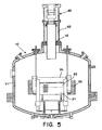
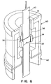
- Figs. 5 and 6 illustrate still another alternate embodiment of the invention.
- a rapid temperature external heater fixture 60 is mounted on a heater support column 62 outside furnace 10 adjacent exit port 12 to provide auxiliary heating for the growing web.
- the holder 34 and solid diffusion source 33 are both positioned within the external heater fixture 60, which provides easier access to these elements in order to facilitate installation and removal of the diffusion sources 33.
- the embodiment of Figs. 5 and 6 eliminates vertical thermal element 31.
- Attached as Appendix A are 14 sheets of drawing illustrating actual fixture details for vertical thermal element 31, source holder 34, rods 36 and ancillary components.
- the invention permits in-situ diffusion of dopant materials into one or both major surfaces of the growing dendritic web emerging from the melt crucible.
- This arrangement eliminates the necessity for providing gaseous dopant diffusion sources and the attendant disadvantages of such diffusion source arrangements.
- the solid planar diffusion source may be easily installed and removed from the source holder, and the relative vertical position of the solid diffusion source 33 can be readily adjusted by means of rods 36 to provide source temperature adjustment.
- the invention eliminates the need for a separate diffusion station for the dendritic web formation process, which renders the production facility more compact and simplifies the installation, initial set-up and process operation when producing dendritic web photovoltaic cells.
Landscapes
- Chemical & Material Sciences (AREA)
- Engineering & Computer Science (AREA)
- Crystallography & Structural Chemistry (AREA)
- Materials Engineering (AREA)
- Metallurgy (AREA)
- Organic Chemistry (AREA)
- Crystals, And After-Treatments Of Crystals (AREA)
- Photovoltaic Devices (AREA)
Claims (18)
- Procédé pour fabriquer un ruban de cristal de silicium photovoltaïque à bande dendritique, comprenant les étapes consistant à:(1) faire croítre un ruban de cristal de silicium à bande dendritique incluant deux surfaces principales et une dendrite délivrée par une source de masse fondue dans un four par tirage du matériau fondu le long d'un trajet partant de la source de fusion et permettant un refroidissement du matériau fondu;(2) exposer directement les deux surfaces principales de la bande en cours de croissance à un matériau dopant solide possédant une forme plane et chauffé à une température de diffusion lorsque la bande en cours de croissance est tirée le long du trajet, et selon lequel le matériau dopant solide plat s'étend partiellement sur la longueur du ruban, et selon lequel le matériau dopant solide comprend un premier élément de matériau dopant disposé de manière à être en vis-à-vis de l'une desdites première et seconde surfaces principales de ladite bande de cristal dendritique et un second élément de matériau dopant disposé de manière à être situé en vis-à-vis de l'autre desdites première et seconde surfaces principales de ladite bande de cristal dendritique de sorte que chacun des premier et second éléments du matériau dopant agit en tant que source de diffusion pour la surface principale, tournée en vis-à-vis de façon correspondante de ladite bande de cristal dendritique en cours de croissance, les premier et second éléments de matériau dopant fournissant des dopants ayant des types de conductivité opposés.
- Procédé selon la revendication 1, selon lequel ladite étape d'exposition (2) inclut l'étape constituant à placer un matériau dopant solide dans un dispositif de retenue adjacent à une source thermique pour chauffer le matériau dopant solide jusqu'à la température de diffusion.
- Procédé selon la revendication 2, dans lequel ladite étape de mise en place inclut les étapes consistant à prévoir un élément thermique solide et à chauffer l'élément thermique.
- Procédé selon la revendication 3, selon lequel ladite étape de chauffage est effectuée en soumettant l'élément thermique à une chaleur contenue dans le four.
- Procédé selon la revendication 3, selon lequel ladite étape de chauffage est exécutée en chauffant l'élément thermique avec une bobine de chauffage.
- Procédé selon la revendication 1, selon lequel ladite étape d'exposition (2) est exécutée dans le four.
- Procédé selon la revendication 1, selon lequel le four comporte un orifice de sortie de la bande; et selon lequel ladite étape d'exposition (2) est exécutée à l'extérieur du four.
- Procédé selon la revendication 7, selon lequel ladite étape d'exposition (2) inclut des étapes consistant. à disposer une source thermique au voisinage de l'orifice de sortie et à placer le matériau dopant solide en contact thermique avec la source thermique au voisinage de l'orifice de sortie.
- Dispositif pour la fabrication d'un ruban de cristal de silicium photovoltaïque à bande dendritique, ledit dispositif comprenant:un four comportant des moyens pour produire une source de masse fondue du matériau de croissance de cristal de silicium, et un orifice de sortie;des moyens pour tirer ledit matériau fondu le long d'un trajet partant de la source de fusion à travers l'orifice de sortie de sorte qu'il se produit une croissance du ruban de cristal de silicium à bande dendritique incluant deux surfaces principales et une dendrite lorsque le matériau fondu est tiré le long du trajet;un matériau dopant solide disposé le long dudit trajet, ledit matériau dopant solide possédant une forme et étant maintenu en vis-à-vis des deux surfaces principales de la bande de cristal de Si dendritique, et dans lequel le matériau dopant solide comprend un premier élément de matériau dopant disposé de manière à être en vis-à-vis de l'une desdites première et seconde surfaces principales de ladite bande de cristal dendritique et un second élément de matériau dopant disposé de manière à être situé en vis-à-vis de l'autre desdites première et seconde surfaces principales de ladite bande de cristal dendritique de sorte que chacun des premier et second éléments du matériau dopant agit en tant que source de diffusion pour la surface principale, tournée en vis-à-vis de façon correspondante de ladite bande de cristal dendritique en cours de croissance, les premier et second éléments de matériau dopant fournissant des dopants ayant des types de conductivité opposés; etdes moyens pour chauffer ledit matériau dopant solide à une température de diffusion de telle sorte que la bande de cristal dendritique en cours de croissance est exposée audit matériau dopant solide pour créer une couche de diffusion dans ladite au moins une desdites deux surfaces principales.
- Dispositif selon la revendication 9, comprenant en outre un dispositif de retenue monté le long du trajet pour recevoir ledit matériau dopant solide.
- Dispositif selon la revendication 10, dans lequel ledit dispositif de retenue est situé dans ledit four.
- Dispositif selon la revendication 10, dans lequel ledit dispositif de retenue est situé à l'extérieur dudit four au voisinage dudit orifice de sortie.
- Dispositif selon la revendication 9, dans lequel lesdits moyens de chauffage dudit matériau dopant solide incluent un élément thermique situé le long dudit trajet et entourant au moins partiellement ledit matériau dopant, ledit matériau dopant solide étant disposé en contact thermique avec ledit élément thermique.
- Dispositif selon la revendication 13, dans lequel lesdits moyens pour chauffer ledit élément thermique comporte en outre une bobine de chauffage pour chauffer ledit élément thermique.
- Dispositif selon la revendication 13, dans lequel lesdits moyens de chauffage sont situés dans ledit four.
- Dispositif selon la revendication 13, dans lequel lesdits moyens de chauffage sont situés à l'extérieur dudit four au voisinage dudit orifice de sortie.
- Procédé selon la revendication 1, selon lequel ledit matériau dopant solide est une bande rectangulaire.
- Dispositif selon la revendication 9, dans lequel ledit matériau dopant solide est une bande rectangulaire.
Priority Applications (6)
| Application Number | Priority Date | Filing Date | Title |
|---|---|---|---|
| CA002216998A CA2216998C (fr) | 1997-10-01 | 1997-10-01 | Distribution in situ d'impuretes dopantes pendant la croissance de bande dendritique d'un ruban a cristaux |
| AU39874/97A AU740188B2 (en) | 1997-10-01 | 1997-10-01 | In-situ diffusion of dopant impurities during dendritic web growth of crystal ribbon |
| BR9704971A BR9704971A (pt) | 1997-10-01 | 1997-10-03 | Processo e aparelho para fabricar um fita de cristal fotovoltaic de estrutura dendrítica |
| DE69729091T DE69729091T2 (de) | 1997-10-01 | 1997-10-09 | In-situ-Diffusion von Dotierstoffen bei dendritisch vernetztem Wachstum eines kristallinen Siliziumbandes |
| ES97117465T ES2217359T3 (es) | 1997-10-01 | 1997-10-09 | Difusion in situ de impurezas dopantes durante el crecimiento de reticula dendritica de una cinta cristalina de silice. |
| EP97117465A EP0908958B1 (fr) | 1997-10-01 | 1997-10-09 | Diffusion in-situ de dopant durant la croissance en réseau dendritique d'un ruban cristal de silicium |
Applications Claiming Priority (4)
| Application Number | Priority Date | Filing Date | Title |
|---|---|---|---|
| CA002216998A CA2216998C (fr) | 1997-10-01 | 1997-10-01 | Distribution in situ d'impuretes dopantes pendant la croissance de bande dendritique d'un ruban a cristaux |
| AU39874/97A AU740188B2 (en) | 1997-10-01 | 1997-10-01 | In-situ diffusion of dopant impurities during dendritic web growth of crystal ribbon |
| BR9704971A BR9704971A (pt) | 1997-10-01 | 1997-10-03 | Processo e aparelho para fabricar um fita de cristal fotovoltaic de estrutura dendrítica |
| EP97117465A EP0908958B1 (fr) | 1997-10-01 | 1997-10-09 | Diffusion in-situ de dopant durant la croissance en réseau dendritique d'un ruban cristal de silicium |
Publications (2)
| Publication Number | Publication Date |
|---|---|
| EP0908958A1 EP0908958A1 (fr) | 1999-04-14 |
| EP0908958B1 true EP0908958B1 (fr) | 2004-05-12 |
Family
ID=27423137
Family Applications (1)
| Application Number | Title | Priority Date | Filing Date |
|---|---|---|---|
| EP97117465A Expired - Lifetime EP0908958B1 (fr) | 1997-10-01 | 1997-10-09 | Diffusion in-situ de dopant durant la croissance en réseau dendritique d'un ruban cristal de silicium |
Country Status (6)
| Country | Link |
|---|---|
| EP (1) | EP0908958B1 (fr) |
| AU (1) | AU740188B2 (fr) |
| BR (1) | BR9704971A (fr) |
| CA (1) | CA2216998C (fr) |
| DE (1) | DE69729091T2 (fr) |
| ES (1) | ES2217359T3 (fr) |
Families Citing this family (2)
| Publication number | Priority date | Publication date | Assignee | Title |
|---|---|---|---|---|
| DE10024710A1 (de) * | 2000-05-18 | 2001-12-20 | Steag Rtp Systems Gmbh | Einstellung von Defektprofilen in Kristallen oder kristallähnlichen Strukturen |
| CN114441579B (zh) * | 2022-01-07 | 2024-05-28 | 攀钢集团研究院有限公司 | 一种连铸坯枝晶间夹杂位置的检测方法 |
Family Cites Families (2)
| Publication number | Priority date | Publication date | Assignee | Title |
|---|---|---|---|---|
| AU602113B2 (en) * | 1987-09-08 | 1990-09-27 | Ebara Solar, Inc. | Purification process for dendritic web silicon crystal growth system and dendritic web silicon crystals made thereby |
| US5106763A (en) * | 1988-11-15 | 1992-04-21 | Mobil Solar Energy Corporation | Method of fabricating solar cells |
-
1997
- 1997-10-01 CA CA002216998A patent/CA2216998C/fr not_active Expired - Fee Related
- 1997-10-01 AU AU39874/97A patent/AU740188B2/en not_active Ceased
- 1997-10-03 BR BR9704971A patent/BR9704971A/pt not_active Application Discontinuation
- 1997-10-09 DE DE69729091T patent/DE69729091T2/de not_active Expired - Fee Related
- 1997-10-09 EP EP97117465A patent/EP0908958B1/fr not_active Expired - Lifetime
- 1997-10-09 ES ES97117465T patent/ES2217359T3/es not_active Expired - Lifetime
Also Published As
| Publication number | Publication date |
|---|---|
| CA2216998C (fr) | 2005-05-03 |
| CA2216998A1 (fr) | 1999-04-01 |
| AU3987497A (en) | 1999-04-22 |
| DE69729091T2 (de) | 2004-09-09 |
| BR9704971A (pt) | 1999-06-01 |
| EP0908958A1 (fr) | 1999-04-14 |
| ES2217359T3 (es) | 2004-11-01 |
| AU740188B2 (en) | 2001-11-01 |
| DE69729091D1 (de) | 2004-06-17 |
Similar Documents
| Publication | Publication Date | Title |
|---|---|---|
| JP2804505B2 (ja) | 板/スラブの形の大きな単結晶の成長のための装置及び方法 | |
| US6299682B1 (en) | Method for producing silicon ingot having directional solidification structure and apparatus for producing the same | |
| CA1215297A (fr) | Methode et appareil pour regler l'atmosphere au voisinage d'une zone de croissance cristalline | |
| EP0068021B1 (fr) | Procede et appareil de formation et de developpement d'un monocristal d'un compose semi-conducteur | |
| US20010004874A1 (en) | Method of producing a crystal sheet, apparatus for use in producing the same, and solar cell | |
| CA1079612A (fr) | Methode et appareil destines a reduire les tensions residuelles des cristaux | |
| WO2003005417A3 (fr) | Procede et appareil servant a la croissance de cristaux semi-conducteurs au moyen d'un support rigide, dopage au carbone, d'une regulation de la resistivite et du gradient de temperature | |
| US4118197A (en) | Cartridge and furnace for crystal growth | |
| US4832922A (en) | Single crystal growing method and apparatus | |
| JP2010504905A (ja) | 結晶シリコン基板を製造するための方法及び装置 | |
| EP3617351B1 (fr) | Dispositif et procédé de croissance horizontale de tranche de silicium | |
| CA1080588A (fr) | Methode de faconnage et d'epitaxie d'un cristal simple a partir de materiaux semiconducteurs | |
| WO1993017158A1 (fr) | Procede et appareil permettant la croissance de cristaux façonnes | |
| JP3002479B2 (ja) | 太陽電池の製造方法 | |
| US6355910B1 (en) | Heating element for heating crucibles and arrangement of heating elements | |
| EP0908958B1 (fr) | Diffusion in-situ de dopant durant la croissance en réseau dendritique d'un ruban cristal de silicium | |
| US3977934A (en) | Silicon manufacture | |
| US6143633A (en) | In-situ diffusion of dopant impurities during dendritic web growth of crystal ribbon | |
| US4267010A (en) | Guidance mechanism | |
| US4861416A (en) | Ribbon growing method and apparatus | |
| US4334948A (en) | Method of and apparatus for growing crystal ribbon | |
| US6180872B1 (en) | Process and apparatus for growing crystalline silicon plates by pulling the plate through a growth member | |
| KR101199562B1 (ko) | 다결정 실리콘 잉곳 제조장치 | |
| MXPA97007686A (en) | In-situ diffusion of boro or phosphorus, during the growth of dendritic membrane of sili tape | |
| JPH11121777A (ja) | 結晶リボンの樹枝状ウェブ成長中のドーピング不純物の拡散 |
Legal Events
| Date | Code | Title | Description |
|---|---|---|---|
| PUAI | Public reference made under article 153(3) epc to a published international application that has entered the european phase |
Free format text: ORIGINAL CODE: 0009012 |
|
| AK | Designated contracting states |
Kind code of ref document: A1 Designated state(s): DE ES FR GB IT NL |
|
| AX | Request for extension of the european patent |
Free format text: AL;LT;LV;RO;SI |
|
| 17P | Request for examination filed |
Effective date: 19990727 |
|
| AKX | Designation fees paid |
Free format text: DE ES FR GB IT NL |
|
| 17Q | First examination report despatched |
Effective date: 20000329 |
|
| GRAP | Despatch of communication of intention to grant a patent |
Free format text: ORIGINAL CODE: EPIDOSNIGR1 |
|
| RTI1 | Title (correction) |
Free format text: IN-SITU DIFFUSION OF DOPANT IMPURITIES DURING DENDRITIC WEB GROWTH OF SILICON CRYSTAL RIBBON |
|
| GRAS | Grant fee paid |
Free format text: ORIGINAL CODE: EPIDOSNIGR3 |
|
| RAP1 | Party data changed (applicant data changed or rights of an application transferred) |
Owner name: EBARA CORPORATION |
|
| GRAA | (expected) grant |
Free format text: ORIGINAL CODE: 0009210 |
|
| AK | Designated contracting states |
Kind code of ref document: B1 Designated state(s): DE ES FR GB IT NL |
|
| REG | Reference to a national code |
Ref country code: GB Ref legal event code: FG4D |
|
| REF | Corresponds to: |
Ref document number: 69729091 Country of ref document: DE Date of ref document: 20040617 Kind code of ref document: P |
|
| PG25 | Lapsed in a contracting state [announced via postgrant information from national office to epo] |
Ref country code: GB Free format text: LAPSE BECAUSE OF NON-PAYMENT OF DUE FEES Effective date: 20041009 |
|
| REG | Reference to a national code |
Ref country code: ES Ref legal event code: FG2A Ref document number: 2217359 Country of ref document: ES Kind code of ref document: T3 |
|
| ET | Fr: translation filed | ||
| PLBE | No opposition filed within time limit |
Free format text: ORIGINAL CODE: 0009261 |
|
| STAA | Information on the status of an ep patent application or granted ep patent |
Free format text: STATUS: NO OPPOSITION FILED WITHIN TIME LIMIT |
|
| PG25 | Lapsed in a contracting state [announced via postgrant information from national office to epo] |
Ref country code: NL Free format text: LAPSE BECAUSE OF NON-PAYMENT OF DUE FEES Effective date: 20050501 |
|
| 26N | No opposition filed |
Effective date: 20050215 |
|
| GBPC | Gb: european patent ceased through non-payment of renewal fee |
Effective date: 20041009 |
|
| NLV4 | Nl: lapsed or anulled due to non-payment of the annual fee |
Effective date: 20050501 |
|
| PG25 | Lapsed in a contracting state [announced via postgrant information from national office to epo] |
Ref country code: FR Free format text: LAPSE BECAUSE OF NON-PAYMENT OF DUE FEES Effective date: 20060630 |
|
| REG | Reference to a national code |
Ref country code: FR Ref legal event code: ST Effective date: 20060630 |
|
| PGFP | Annual fee paid to national office [announced via postgrant information from national office to epo] |
Ref country code: ES Payment date: 20071026 Year of fee payment: 11 Ref country code: DE Payment date: 20071130 Year of fee payment: 11 |
|
| PGFP | Annual fee paid to national office [announced via postgrant information from national office to epo] |
Ref country code: IT Payment date: 20071029 Year of fee payment: 11 |
|
| PG25 | Lapsed in a contracting state [announced via postgrant information from national office to epo] |
Ref country code: FR Free format text: LAPSE BECAUSE OF NON-PAYMENT OF DUE FEES Effective date: 20041031 |
|
| PG25 | Lapsed in a contracting state [announced via postgrant information from national office to epo] |
Ref country code: IT Free format text: LAPSE BECAUSE OF NON-PAYMENT OF DUE FEES Effective date: 20081009 Ref country code: DE Free format text: LAPSE BECAUSE OF NON-PAYMENT OF DUE FEES Effective date: 20090501 |
|
| REG | Reference to a national code |
Ref country code: ES Ref legal event code: FD2A Effective date: 20081010 |
|
| PG25 | Lapsed in a contracting state [announced via postgrant information from national office to epo] |
Ref country code: ES Free format text: LAPSE BECAUSE OF NON-PAYMENT OF DUE FEES Effective date: 20081010 |