EP0910868B1 - Procede et dispositif de traitement sans contact d'un substrat semi-conducteur sous forme de plaquette - Google Patents
Procede et dispositif de traitement sans contact d'un substrat semi-conducteur sous forme de plaquette Download PDFInfo
- Publication number
- EP0910868B1 EP0910868B1 EP97929595A EP97929595A EP0910868B1 EP 0910868 B1 EP0910868 B1 EP 0910868B1 EP 97929595 A EP97929595 A EP 97929595A EP 97929595 A EP97929595 A EP 97929595A EP 0910868 B1 EP0910868 B1 EP 0910868B1
- Authority
- EP
- European Patent Office
- Prior art keywords
- side sections
- substrate
- wafer
- gas
- semiconductor substrate
- Prior art date
- Legal status (The legal status is an assumption and is not a legal conclusion. Google has not performed a legal analysis and makes no representation as to the accuracy of the status listed.)
- Expired - Lifetime
Links
Images

Classifications
-
- C—CHEMISTRY; METALLURGY
- C23—COATING METALLIC MATERIAL; COATING MATERIAL WITH METALLIC MATERIAL; CHEMICAL SURFACE TREATMENT; DIFFUSION TREATMENT OF METALLIC MATERIAL; COATING BY VACUUM EVAPORATION, BY SPUTTERING, BY ION IMPLANTATION OR BY CHEMICAL VAPOUR DEPOSITION, IN GENERAL; INHIBITING CORROSION OF METALLIC MATERIAL OR INCRUSTATION IN GENERAL
- C23C—COATING METALLIC MATERIAL; COATING MATERIAL WITH METALLIC MATERIAL; SURFACE TREATMENT OF METALLIC MATERIAL BY DIFFUSION INTO THE SURFACE, BY CHEMICAL CONVERSION OR SUBSTITUTION; COATING BY VACUUM EVAPORATION, BY SPUTTERING, BY ION IMPLANTATION OR BY CHEMICAL VAPOUR DEPOSITION, IN GENERAL
- C23C16/00—Chemical coating by decomposition of gaseous compounds, without leaving reaction products of surface material in the coating, i.e. chemical vapour deposition [CVD] processes
- C23C16/44—Chemical coating by decomposition of gaseous compounds, without leaving reaction products of surface material in the coating, i.e. chemical vapour deposition [CVD] processes characterised by the method of coating
- C23C16/46—Chemical coating by decomposition of gaseous compounds, without leaving reaction products of surface material in the coating, i.e. chemical vapour deposition [CVD] processes characterised by the method of coating characterised by the method used for heating the substrate
-
- H—ELECTRICITY
- H10—SEMICONDUCTOR DEVICES; ELECTRIC SOLID-STATE DEVICES NOT OTHERWISE PROVIDED FOR
- H10P—GENERIC PROCESSES OR APPARATUS FOR THE MANUFACTURE OR TREATMENT OF DEVICES COVERED BY CLASS H10
- H10P95/00—Generic processes or apparatus for manufacture or treatments not covered by the other groups of this subclass
-
- H—ELECTRICITY
- H10—SEMICONDUCTOR DEVICES; ELECTRIC SOLID-STATE DEVICES NOT OTHERWISE PROVIDED FOR
- H10P—GENERIC PROCESSES OR APPARATUS FOR THE MANUFACTURE OR TREATMENT OF DEVICES COVERED BY CLASS H10
- H10P72/00—Handling or holding of wafers, substrates or devices during manufacture or treatment thereof
- H10P72/04—Apparatus for manufacture or treatment
- H10P72/0431—Apparatus for thermal treatment
- H10P72/0434—Apparatus for thermal treatment mainly by convection
-
- H—ELECTRICITY
- H10—SEMICONDUCTOR DEVICES; ELECTRIC SOLID-STATE DEVICES NOT OTHERWISE PROVIDED FOR
- H10P—GENERIC PROCESSES OR APPARATUS FOR THE MANUFACTURE OR TREATMENT OF DEVICES COVERED BY CLASS H10
- H10P72/00—Handling or holding of wafers, substrates or devices during manufacture or treatment thereof
- H10P72/30—Handling or holding of wafers, substrates or devices during manufacture or treatment thereof for conveying, e.g. between different workstations
- H10P72/36—Handling or holding of wafers, substrates or devices during manufacture or treatment thereof for conveying, e.g. between different workstations using air tracks
Definitions
- the present invention relates to a method for contactless treatment of a semiconductor wafer substrate, comprising placing said substrate in an apparatus which at least partially encloses said substrate and applying two gas streams, in opposing directions, from first and second side sections located opposite one another, to the two opposing sides of the semiconductor substrate.
- Netherlands Laid Open Application 8402410 in which, furthermore, reference is made to Netherlands Laid Open Applications 8103979, 8200753 and 8203318.
- Heating is frequently necessary when treating semiconductor substrates. Heating can involve annealing or raising the temperature to make deposition or other processes possible.
- wafers are to this end placed in furnaces and then heated.
- this method is adequate, it has at least two disadvantages. Firstly, a method of this type is never contactless, that is to say certain points of the wafer must always be supported. Secondly, it takes a relatively long time to heat a wafer. This is due not so much to the thermal capacity of the wafer itself as to the thermal capacity of the furnace in which the wafers are placed.
- US patent 4 622 918 discloses an apparatus wherein a wafer is fed through between a number of columns located some distance apart. Sets of columns located opposite one another, between which the wafer moves, are likewise some distance apart. In the gap between the sets of columns, heating is effected by means of a lamp some distance away. This apparatus also has the drawback of relatively slow energy-consuming heating by means of lamps.
- the aim of the present invention is to provide a method with which contactless heating of semiconductor substrates to relatively high temperature within a relatively short time is possible.
- Introduction of the wafer into the enclosing apparatus described above is effected by moving the side sections apart.
- the wafer is placed between the side sections when the latter have been moved apart.
- Supporting means can optionally be present to fix the wafer in such a position.
- the side sections then move towards one another and the function of the supporting means is taken over by the gas stream moving out of the side sections concerned. As a result, the wafer moves away from the supporting means.
- a temperature difference is applied over the wafer.
- One of the side sections is heated to a relatively high temperature, whilst the other of the side sections is heated to a relatively low temperature. It has been found that, as a result of the thermal behaviour of the enclosing apparatus, the wafer will assume a temperature which is dependent on the position of the wafer with respect to the two heated side sections. If the two side sections are equidistant from the wafer and the same gas is present on both sides, the temperature will fairly accurately be the average of the values of the temperatures of each of the side sections.
- the temperature will change correspondingly.
- these values can be set very accurately. After all, it has been found that these values are mainly dependent on the position of the wafer in the enclosing apparatus. As already indicated above, the position of the wafer in the tunnel-like apparatus is accurately related to the quantity and type of gas supplied from the related side sections.
- At least one of the side sections is provided with heating means for heating said section(s) to above 250 °C.
- heating means for heating said section(s) to above 250 °C.
- the related side section is provided with a number of spaced gas feed channels in order to provide uniform metering of the gas and more particularly process gas.
- a construction of this type can, for example, be achieved by providing porous plates.
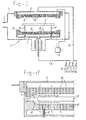
- FIG. 1 the apparatus according to the invention is indicated in its entirety by 1.
- This apparatus is provided with an inlet 4, which can be connected, in a manner not shown in more detail, to a 'load lock' or a cluster system for further treatment of semiconductor substrates.
- the actual apparatus according to the invention consisting of the first and second side sections 6 and 7, respectively, is accommodated in a pressure vessel 2 for carrying out a process in a specific environment or under elevated or reduced pressure.
- the first side section 6 is joined rigidly to the pressure vessel 2.
- a heating coil 8, which is connected to a control 5, is mounted inside said first side section.
- a gas supply line 12 is also present, which gas supply line is connected to the gas feeds 10 which consist of a number of uniformly distributed passages.
- Second side section 7 is constructed correspondingly. Supporting pins 11 for supporting the semiconductor substrate extend through the second side section 7.
- the various features are so dimensioned that when the two side sections are in the closed position, the semiconductor substrate 3 is no longer supported by the supporting pins 11 but by the gas streams which move towards the semiconductor substrate 3 from both side sections.
- Gas passages 10 in the second side section 7 are connected to a gas supply line 14, which is connected to a source 15.
- the wafer 3 is placed on the supporting pins 11, as is also shown in Fig. 2.
- the second side section 7 is then moved up and the situation as shown in Fig. 2 is obtained.
- the wafer 3 is accurately positioned in the centre between the two side sections 6 and 7 by the gas streams issuing from the passages 10 in said two side sections. Deviation in the position is possible by means of adjusting the gas flow.
- the side sections are heated by operation of the heating elements 8 and 9 and it has been found that this heat is transferred to the wafer with negligible loss.
- Fig. 3 In this case both side sections have been heated to a temperature of approximately 1200 °C. It has been found that wafer 3 has the same temperature within four seconds. Because wafer 3 is not supported and is heated uniformly, no thermal stresses will be produced, as a result of which there is no question of distortion.
- the relevant gases are supplied as process gases through the passages 10.
- the deposition temperature of material from the silane gas issuing from source 15 is 625 °C (900 K)
- 700 K virtually no deposition of material from the gas will take place, so that the passages 10 concerned will not clog.
- the wafer is found accurately to assume a temperature which is midway between that of the first side section 6 and that of the second side section 7, this being the desired temperature of 900 K.
- Fig. 2 As a result of the flow of the gases shown (Fig. 2), it is largely precluded that gas issuing from the second side section 7 will enter the -first hot side section 6 and deposit there. In any event it has not been found that passages 10 in the first side section 6 clog.
- the upper side section is provided with a large number of gas passages, whilst this is not the case for side section 7. In this way an accurately controlled gas purge flowing radially outwards can be provided and deposition on section 6 prevented.
- the side section 7 is at a lower temperature, it is not necessary to use the pins described above.
- the wafer can be placed directly on side section 7. In such a case it is not even desirable to use pins, because in a set-up of this type the 'device side' faces downwards.
- the side sections can be moved away from one another again and the wafer removed. Cooling takes place equally as rapidly as heating without any damage over the entire extent of the wafer.
- the distance between a wafer and the surface of the relevant side sections from which gases issue is 1 mm or less, for example a few tenths of millimetres.
- Such a rotation can, for example, be achieved by positioning one or more of the channels 10 at an angle with respect to the vertical, as a result of which a spiral gas flow is generated.
Landscapes
- Chemical & Material Sciences (AREA)
- General Chemical & Material Sciences (AREA)
- Chemical Kinetics & Catalysis (AREA)
- Engineering & Computer Science (AREA)
- Materials Engineering (AREA)
- Mechanical Engineering (AREA)
- Metallurgy (AREA)
- Organic Chemistry (AREA)
- Container, Conveyance, Adherence, Positioning, Of Wafer (AREA)
Abstract
Claims (12)
- Procédé de traitement sans contact d'un substrat semi-conducteur en plaquette (3) comprenant le placement dudit substrat dans un appareil qui entoure au moins partiellement ledit substrat et l'application de deux jets de gaz dans des directions opposées, depuis des première et seconde sections latérales (6, 7) situées à l'opposé l'une de l'autre, sur les deux côtés opposés du substrat semi-conducteur pour positionner ledit substrat, dans lequel l'espacement entre chacune desdites première et seconde sections latérales et le substrat semi-conducteur est établi au maximum à 1 mm, caractérisé en ce que au moins l'une desdites sections latérales est chauffée à une température supérieure à 200°C, et lesdites sections latérales peuvent se déplacer l'une par rapport à l'autre, le substrat semi-conducteur est introduit à une faible température entre les deux sections latérales positionnées à une distance relativement grande l'une de l'autre, après quoi les sections latérales sont déplacées en direction l'une de l'autre pour que les jets de gaz supportent le substrat et les jets de gaz sont appliqués de telle sorte que le gaz est distribué uniformément sur la surface du substrat semi-conducteur à traiter de façon à chauffer le substrat.
- Procédé selon la revendication 1, dans lequel dans la position de départ, le substrat est supporté par des moyens mécaniques auxiliaires (11).
- Procédé selon l'une des revendications précédentes, dans lequel le substrat est soumis à un mouvement de rotation.
- Procédé selon l'une des revendications précédentes, dans lequel au moins l'un desdits jets de gaz comprend un gaz de traitement.
- Procédé selon la revendication 4, dans lequel la première section latérale de l'appareil d'enceinte est amenée à une première température et la seconde section latérale, qui est opposée à ladite première section latérale, est amenée à une seconde température plus basse, et dans lequel le gaz de traitement est appliqué depuis la seconde section latérale.
- Procédé selon la revendication 5, dans lequel la différence de température entre la plaquette et l'une desdites sections latérales est établie à au moins 150°C.
- Procédé selon la revendication 6, dans lequel la différence de température entre la plaquette et l'une desdites sections latérales est établie à au moins 200°C.
- Procédé selon l'une des revendications 5 à 7, dans lequel le substrat est déplacé depuis le point au centre entre les sections latérales en contrôlant l'écoulement des gaz.
- Procédé selon l'une des revendications 5 à 8, dans lequel des gaz ayant différents transferts de chaleur sont utilisés depuis la première section latérale et depuis la seconde section latérale.
- Appareil (1) pour le traitement sans contact d'un substrat semi-conducteur en plaquette (3) comprenant une partie d'enceinte munie d'au moins des première et seconde sections latérales (6, 7) pour loger un substrat semi-conducteur (3) entre elles, et ayant des passages (10) pour appliquer du gaz pour positionner ladite plaquette entre lesdites sections latérales, caractérisé en ce que au moins l'une desdites sections latérales est munie de moyens de chauffage (8, 9) pour chauffer ladite ou lesdites section(s) jusqu'à plus de 250°C, et en ce que lesdits passages d'alimentation en gaz sont prévus de telle sorte qu'une distribution uniforme d'un gaz sur la surface du substrat semi-conducteur à traiter puisse être obtenue, et en ce que lesdites sections latérales peuvent se déplacer l'une par rapport à l'autre tout en étant chauffées, entre une position séparée pour faciliter le chargement d'un substrat semi-conducteur entre lesdites sections latérales, et une position fermée dans laquelle un substrat semi-conducteur est supporté par les jets de gaz et espacé de 1 mm ou moins desdites sections latérales.
- Appareil selon la revendication 10, dans lequel des moyens de support (11) sont présents, lesquels peuvent être utilisés pour supporter le substrat lorsque lesdites sections latérales sont positionnées à une distance relativement grande l'une de l'autre.
- Appareil selon la revendication 11, dans lequel lesdits passages d'alimentation en gaz (10) sont prévus sous la forme d'une plaque poreuse.
Applications Claiming Priority (3)
| Application Number | Priority Date | Filing Date | Title |
|---|---|---|---|
| NL1003538 | 1996-07-08 | ||
| NL1003538A NL1003538C2 (nl) | 1996-07-08 | 1996-07-08 | Werkwijze en inrichting voor het contactloos behandelen van een schijfvormig halfgeleidersubstraat. |
| PCT/NL1997/000398 WO1998001890A1 (fr) | 1996-07-08 | 1997-07-08 | Procede et dispositif de traitement sans contact d'un substrat semi-conducteur sous forme de plaquette |
Publications (2)
| Publication Number | Publication Date |
|---|---|
| EP0910868A1 EP0910868A1 (fr) | 1999-04-28 |
| EP0910868B1 true EP0910868B1 (fr) | 2004-10-13 |
Family
ID=19763169
Family Applications (1)
| Application Number | Title | Priority Date | Filing Date |
|---|---|---|---|
| EP97929595A Expired - Lifetime EP0910868B1 (fr) | 1996-07-08 | 1997-07-08 | Procede et dispositif de traitement sans contact d'un substrat semi-conducteur sous forme de plaquette |
Country Status (8)
| Country | Link |
|---|---|
| EP (1) | EP0910868B1 (fr) |
| JP (1) | JPH11514154A (fr) |
| KR (1) | KR100335282B1 (fr) |
| AU (1) | AU3361797A (fr) |
| DE (1) | DE69731199T2 (fr) |
| NL (1) | NL1003538C2 (fr) |
| TW (1) | TW493214B (fr) |
| WO (1) | WO1998001890A1 (fr) |
Families Citing this family (53)
| Publication number | Priority date | Publication date | Assignee | Title |
|---|---|---|---|---|
| US6183565B1 (en) | 1997-07-08 | 2001-02-06 | Asm International N.V | Method and apparatus for supporting a semiconductor wafer during processing |
| NL1011017C2 (nl) * | 1999-01-13 | 2000-07-31 | Asm Int | Inrichting voor het positioneren van een wafer. |
| NL1011487C2 (nl) | 1999-03-08 | 2000-09-18 | Koninkl Philips Electronics Nv | Werkwijze en inrichting voor het roteren van een wafer. |
| NL1012004C2 (nl) * | 1999-05-07 | 2000-11-13 | Asm Int | Werkwijze voor het verplaatsen van wafers alsmede ring. |
| US6803546B1 (en) | 1999-07-08 | 2004-10-12 | Applied Materials, Inc. | Thermally processing a substrate |
| NL1013938C2 (nl) | 1999-12-23 | 2001-06-26 | Asm Int | Inrichting voor het behandelen van een wafer. |
| NL1013984C2 (nl) * | 1999-12-29 | 2001-07-02 | Asm Int | Werkwijze en inrichting voor het behandelen van substraten. |
| NL1013989C2 (nl) * | 1999-12-29 | 2001-07-02 | Asm Int | Werkwijze en inrichting voor het behandelen van een wafer. |
| US7494927B2 (en) | 2000-05-15 | 2009-02-24 | Asm International N.V. | Method of growing electrical conductors |
| US6679951B2 (en) | 2000-05-15 | 2004-01-20 | Asm Intenational N.V. | Metal anneal with oxidation prevention |
| WO2001088972A1 (fr) | 2000-05-15 | 2001-11-22 | Asm Microchemistry Oy | Procede d'elaboration de circuits integres |
| DE10024710A1 (de) * | 2000-05-18 | 2001-12-20 | Steag Rtp Systems Gmbh | Einstellung von Defektprofilen in Kristallen oder kristallähnlichen Strukturen |
| EP1290720A1 (fr) | 2000-06-16 | 2003-03-12 | Applied Materials, Inc. | Nettoyeur carrousel reconfigurable integre pour nettoyage au mouille ou a sec d'un substrat |
| KR100838874B1 (ko) * | 2000-07-06 | 2008-06-16 | 어플라이드 머티어리얼스, 인코포레이티드 | 기판을 열 처리하는 시스템 및 방법 |
| US6592942B1 (en) | 2000-07-07 | 2003-07-15 | Asm International N.V. | Method for vapour deposition of a film onto a substrate |
| JP2002343708A (ja) * | 2001-05-21 | 2002-11-29 | Toshiba Corp | 基板処理装置および熱処理方法 |
| JP2004536272A (ja) * | 2001-06-08 | 2004-12-02 | アイクストロン、アーゲー | 扁平物体の短時間熱処理方法と装置 |
| US6899111B2 (en) * | 2001-06-15 | 2005-05-31 | Applied Materials, Inc. | Configurable single substrate wet-dry integrated cluster cleaner |
| US6887803B2 (en) * | 2001-11-08 | 2005-05-03 | Wafermasters, Inc. | Gas-assisted rapid thermal processing |
| US20030168174A1 (en) | 2002-03-08 | 2003-09-11 | Foree Michael Todd | Gas cushion susceptor system |
| US7104578B2 (en) | 2002-03-15 | 2006-09-12 | Asm International N.V. | Two level end effector |
| US6952889B2 (en) * | 2002-11-05 | 2005-10-11 | Wafermasters, Inc. | Forced convection assisted rapid thermal furnace |
| US7153772B2 (en) * | 2003-06-12 | 2006-12-26 | Asm International N.V. | Methods of forming silicide films in semiconductor devices |
| US7181132B2 (en) | 2003-08-20 | 2007-02-20 | Asm International N.V. | Method and system for loading substrate supports into a substrate holder |
| US6818517B1 (en) | 2003-08-29 | 2004-11-16 | Asm International N.V. | Methods of depositing two or more layers on a substrate in situ |
| US7022627B2 (en) | 2003-10-31 | 2006-04-04 | Asm International N.V. | Method for the heat treatment of substrates |
| US7410355B2 (en) | 2003-10-31 | 2008-08-12 | Asm International N.V. | Method for the heat treatment of substrates |
| US6883250B1 (en) | 2003-11-04 | 2005-04-26 | Asm America, Inc. | Non-contact cool-down station for wafers |
| US6940047B2 (en) | 2003-11-14 | 2005-09-06 | Asm International N.V. | Heat treatment apparatus with temperature control system |
| US7329114B2 (en) | 2004-01-20 | 2008-02-12 | Komag, Inc. | Isothermal imprint embossing system |
| US7686606B2 (en) | 2004-01-20 | 2010-03-30 | Wd Media, Inc. | Imprint embossing alignment system |
| US7217670B2 (en) | 2004-11-22 | 2007-05-15 | Asm International N.V. | Dummy substrate for thermal reactor |
| US8025922B2 (en) | 2005-03-15 | 2011-09-27 | Asm International N.V. | Enhanced deposition of noble metals |
| US7666773B2 (en) | 2005-03-15 | 2010-02-23 | Asm International N.V. | Selective deposition of noble metal thin films |
| US8278176B2 (en) | 2006-06-07 | 2012-10-02 | Asm America, Inc. | Selective epitaxial formation of semiconductor films |
| US11136667B2 (en) * | 2007-01-08 | 2021-10-05 | Eastman Kodak Company | Deposition system and method using a delivery head separated from a substrate by gas pressure |
| DE102007053108A1 (de) | 2007-05-02 | 2008-11-06 | IHP GmbH - Innovations for High Performance Microelectronics/Institut für innovative Mikroelektronik | Verfahren zum thermischen Behandeln von Wafern |
| US9379011B2 (en) | 2008-12-19 | 2016-06-28 | Asm International N.V. | Methods for depositing nickel films and for making nickel silicide and nickel germanide |
| US7927942B2 (en) | 2008-12-19 | 2011-04-19 | Asm International N.V. | Selective silicide process |
| JP2011091386A (ja) * | 2009-09-24 | 2011-05-06 | Semiconductor Energy Lab Co Ltd | 熱処理装置、熱処理方法及び半導体装置の作製方法 |
| US9330685B1 (en) | 2009-11-06 | 2016-05-03 | WD Media, LLC | Press system for nano-imprinting of recording media with a two step pressing method |
| US8402638B1 (en) | 2009-11-06 | 2013-03-26 | Wd Media, Inc. | Press system with embossing foil free to expand for nano-imprinting of recording media |
| US8496466B1 (en) | 2009-11-06 | 2013-07-30 | WD Media, LLC | Press system with interleaved embossing foil holders for nano-imprinting of recording media |
| US8871617B2 (en) | 2011-04-22 | 2014-10-28 | Asm Ip Holding B.V. | Deposition and reduction of mixed metal oxide thin films |
| US9607842B1 (en) | 2015-10-02 | 2017-03-28 | Asm Ip Holding B.V. | Methods of forming metal silicides |
| US11854842B2 (en) * | 2016-03-18 | 2023-12-26 | Acm Research (Shanghai), Inc. | Substrate heat treatment apparatus |
| US10851457B2 (en) * | 2017-08-31 | 2020-12-01 | Lam Research Corporation | PECVD deposition system for deposition on selective side of the substrate |
| JP7178177B2 (ja) * | 2018-03-22 | 2022-11-25 | 東京エレクトロン株式会社 | 基板処理装置 |
| WO2021034508A1 (fr) | 2019-08-16 | 2021-02-25 | Lam Research Corporation | Dépôt spatialement accordable pour compensation intérieure de cambrure différentielle de tranche |
| KR102953798B1 (ko) | 2020-06-24 | 2026-04-15 | 에이에스엠 아이피 홀딩 비.브이. | 몰리브덴을 포함하는 막의 기상 증착 |
| CN114520175B (zh) * | 2020-11-18 | 2025-06-27 | 致茂电子(苏州)有限公司 | 具备浮动定位功能的芯片移载装置及芯片浮动定位方法 |
| CN112701078A (zh) * | 2020-12-28 | 2021-04-23 | 广东先导先进材料股份有限公司 | 晶片取放装置 |
| WO2026023006A1 (fr) * | 2024-07-25 | 2026-01-29 | 株式会社Kokusai Electric | Dispositif de traitement de substrat, procédé de traitement de substrat, procédé de fabrication de dispositif à semi-conducteur et programme |
Citations (4)
| Publication number | Priority date | Publication date | Assignee | Title |
|---|---|---|---|---|
| NL8103979A (nl) * | 1981-08-26 | 1983-03-16 | Bok Edward | Methode en inrichting voor het aanbrengen van een film vloeibaar medium op een substraat. |
| NL8200753A (nl) * | 1982-02-24 | 1983-09-16 | Integrated Automation | Methode en inrichting voor het aanbrengen van een coating op een substraat of tape. |
| NL8203318A (nl) * | 1982-08-24 | 1984-03-16 | Integrated Automation | Inrichting voor processing van substraten. |
| NL8402410A (nl) * | 1984-08-01 | 1986-03-03 | Bok Edward | Verbeterde proces installatie met double-floating transport en processing van wafers en tape. |
Family Cites Families (3)
| Publication number | Priority date | Publication date | Assignee | Title |
|---|---|---|---|---|
| US4622918A (en) * | 1983-01-31 | 1986-11-18 | Integrated Automation Limited | Module for high vacuum processing |
| JPS59215718A (ja) * | 1983-05-23 | 1984-12-05 | Kokusai Electric Co Ltd | 半導体基板の赤外線熱処理装置 |
| KR0155545B1 (ko) * | 1988-06-27 | 1998-12-01 | 고다까 토시오 | 기판의 열처리 장치 |
-
1996
- 1996-07-08 NL NL1003538A patent/NL1003538C2/nl not_active IP Right Cessation
-
1997
- 1997-07-08 JP JP10505093A patent/JPH11514154A/ja active Pending
- 1997-07-08 AU AU33617/97A patent/AU3361797A/en not_active Abandoned
- 1997-07-08 WO PCT/NL1997/000398 patent/WO1998001890A1/fr not_active Ceased
- 1997-07-08 EP EP97929595A patent/EP0910868B1/fr not_active Expired - Lifetime
- 1997-07-08 KR KR1019980710838A patent/KR100335282B1/ko not_active Expired - Lifetime
- 1997-07-08 DE DE69731199T patent/DE69731199T2/de not_active Expired - Lifetime
-
1998
- 1998-01-09 TW TW087100333A patent/TW493214B/zh not_active IP Right Cessation
Patent Citations (4)
| Publication number | Priority date | Publication date | Assignee | Title |
|---|---|---|---|---|
| NL8103979A (nl) * | 1981-08-26 | 1983-03-16 | Bok Edward | Methode en inrichting voor het aanbrengen van een film vloeibaar medium op een substraat. |
| NL8200753A (nl) * | 1982-02-24 | 1983-09-16 | Integrated Automation | Methode en inrichting voor het aanbrengen van een coating op een substraat of tape. |
| NL8203318A (nl) * | 1982-08-24 | 1984-03-16 | Integrated Automation | Inrichting voor processing van substraten. |
| NL8402410A (nl) * | 1984-08-01 | 1986-03-03 | Bok Edward | Verbeterde proces installatie met double-floating transport en processing van wafers en tape. |
Non-Patent Citations (1)
| Title |
|---|
| The Oxford Encyclopedic English Dictionary, Clarendon Press, Oxford, 1991, page 1577 * |
Also Published As
| Publication number | Publication date |
|---|---|
| AU3361797A (en) | 1998-02-02 |
| DE69731199D1 (de) | 2004-11-18 |
| KR100335282B1 (ko) | 2002-07-18 |
| DE69731199T2 (de) | 2005-03-10 |
| NL1003538C2 (nl) | 1998-01-12 |
| EP0910868A1 (fr) | 1999-04-28 |
| JPH11514154A (ja) | 1999-11-30 |
| WO1998001890A1 (fr) | 1998-01-15 |
| KR20000022406A (ko) | 2000-04-25 |
| TW493214B (en) | 2002-07-01 |
Similar Documents
| Publication | Publication Date | Title |
|---|---|---|
| EP0910868B1 (fr) | Procede et dispositif de traitement sans contact d'un substrat semi-conducteur sous forme de plaquette | |
| US6183565B1 (en) | Method and apparatus for supporting a semiconductor wafer during processing | |
| CN100409402C (zh) | 快速热处理的快速环境转换系统和方法 | |
| JP2662722B2 (ja) | バッチ式熱処理装置 | |
| JP4174837B2 (ja) | 縦型熱処理炉 | |
| EP1258909B1 (fr) | Procédé et appareillage pour le traitement thermique des substrats | |
| US20070243317A1 (en) | Thermal Processing System and Configurable Vertical Chamber | |
| WO1994017353B1 (fr) | Appareil de traitement thermique rapide pour le traitement de tranches de semiconducteurs | |
| KR100457348B1 (ko) | 단일 웨이퍼 어닐링 오븐 | |
| JP2007515054A (ja) | 回転可能な注入器を含む交差流れ注入システムを備えた熱処理システム | |
| JP2009542000A5 (fr) | ||
| US6877250B2 (en) | Apparatus, method and system for the treatment of a wafer | |
| JP2002222806A (ja) | 基板処理装置 | |
| JPH04179223A (ja) | 熱処理装置 | |
| KR20130142963A (ko) | 열처리 장치 | |
| JP3115164B2 (ja) | 熱処理装置 | |
| KR20050083837A (ko) | 강제 대류가 지원된 급속 열로 | |
| KR100239405B1 (ko) | 반도체 제조장치 | |
| JPH0420253B2 (fr) | ||
| JP3510329B2 (ja) | 熱処理装置 | |
| JPS60152675A (ja) | 縦型拡散炉型気相成長装置 | |
| JPS60165379A (ja) | 連続型気相成長方法および装置 | |
| KR200365533Y1 (ko) | 저압 화상기상증착 장치의 반응로 | |
| JP2005340236A (ja) | 基板処理装置 | |
| KR19980021439A (ko) | 반도체 제조장비의 확산로장치 및 열공정 진행방법 |
Legal Events
| Date | Code | Title | Description |
|---|---|---|---|
| PUAI | Public reference made under article 153(3) epc to a published international application that has entered the european phase |
Free format text: ORIGINAL CODE: 0009012 |
|
| 17P | Request for examination filed |
Effective date: 19990108 |
|
| AK | Designated contracting states |
Kind code of ref document: A1 Designated state(s): DE FR GB |
|
| 17Q | First examination report despatched |
Effective date: 20030627 |
|
| GRAP | Despatch of communication of intention to grant a patent |
Free format text: ORIGINAL CODE: EPIDOSNIGR1 |
|
| GRAS | Grant fee paid |
Free format text: ORIGINAL CODE: EPIDOSNIGR3 |
|
| GRAA | (expected) grant |
Free format text: ORIGINAL CODE: 0009210 |
|
| RAP1 | Party data changed (applicant data changed or rights of an application transferred) |
Owner name: ASM INTERNATIONAL N.V. |
|
| AK | Designated contracting states |
Kind code of ref document: B1 Designated state(s): DE FR GB |
|
| REG | Reference to a national code |
Ref country code: GB Ref legal event code: FG4D |
|
| REF | Corresponds to: |
Ref document number: 69731199 Country of ref document: DE Date of ref document: 20041118 Kind code of ref document: P |
|
| PLBE | No opposition filed within time limit |
Free format text: ORIGINAL CODE: 0009261 |
|
| STAA | Information on the status of an ep patent application or granted ep patent |
Free format text: STATUS: NO OPPOSITION FILED WITHIN TIME LIMIT |
|
| ET | Fr: translation filed | ||
| 26N | No opposition filed |
Effective date: 20050714 |
|
| PGFP | Annual fee paid to national office [announced via postgrant information from national office to epo] |
Ref country code: GB Payment date: 20090826 Year of fee payment: 13 |
|
| GBPC | Gb: european patent ceased through non-payment of renewal fee |
Effective date: 20100708 |
|
| PG25 | Lapsed in a contracting state [announced via postgrant information from national office to epo] |
Ref country code: GB Free format text: LAPSE BECAUSE OF NON-PAYMENT OF DUE FEES Effective date: 20100708 |
|
| REG | Reference to a national code |
Ref country code: FR Ref legal event code: PLFP Year of fee payment: 19 |
|
| REG | Reference to a national code |
Ref country code: FR Ref legal event code: PLFP Year of fee payment: 20 |
|
| PGFP | Annual fee paid to national office [announced via postgrant information from national office to epo] |
Ref country code: FR Payment date: 20160613 Year of fee payment: 20 |
|
| PGFP | Annual fee paid to national office [announced via postgrant information from national office to epo] |
Ref country code: DE Payment date: 20160705 Year of fee payment: 20 |
|
| REG | Reference to a national code |
Ref country code: DE Ref legal event code: R071 Ref document number: 69731199 Country of ref document: DE |