EP0911653A1 - Système d'immersion - Google Patents
Système d'immersion Download PDFInfo
- Publication number
- EP0911653A1 EP0911653A1 EP98115824A EP98115824A EP0911653A1 EP 0911653 A1 EP0911653 A1 EP 0911653A1 EP 98115824 A EP98115824 A EP 98115824A EP 98115824 A EP98115824 A EP 98115824A EP 0911653 A1 EP0911653 A1 EP 0911653A1
- Authority
- EP
- European Patent Office
- Prior art keywords
- lens
- refractive index
- immersion system
- layer
- wavelength
- Prior art date
- Legal status (The legal status is an assumption and is not a legal conclusion. Google has not performed a legal analysis and makes no representation as to the accuracy of the status listed.)
- Granted
Links
- 238000007654 immersion Methods 0.000 title claims abstract description 45
- 239000004065 semiconductor Substances 0.000 claims abstract description 50
- 239000000463 material Substances 0.000 claims abstract description 31
- 230000005855 radiation Effects 0.000 claims abstract description 17
- 230000005670 electromagnetic radiation Effects 0.000 claims abstract description 13
- 239000010410 layer Substances 0.000 claims description 28
- 239000011241 protective layer Substances 0.000 claims description 8
- 229910001218 Gallium arsenide Inorganic materials 0.000 claims description 5
- 230000001939 inductive effect Effects 0.000 claims description 4
- 235000012431 wafers Nutrition 0.000 description 14
- 239000011521 glass Substances 0.000 description 6
- 229920003023 plastic Polymers 0.000 description 4
- RVTZCBVAJQQJTK-UHFFFAOYSA-N oxygen(2-);zirconium(4+) Chemical compound [O-2].[O-2].[Zr+4] RVTZCBVAJQQJTK-UHFFFAOYSA-N 0.000 description 3
- 229910001928 zirconium oxide Inorganic materials 0.000 description 3
- 229910018072 Al 2 O 3 Inorganic materials 0.000 description 2
- 239000000853 adhesive Substances 0.000 description 2
- 230000001070 adhesive effect Effects 0.000 description 2
- 238000011161 development Methods 0.000 description 2
- 230000018109 developmental process Effects 0.000 description 2
- 239000010432 diamond Substances 0.000 description 2
- 229910003460 diamond Inorganic materials 0.000 description 2
- 238000004519 manufacturing process Methods 0.000 description 2
- 229910000679 solder Inorganic materials 0.000 description 2
- 238000004544 sputter deposition Methods 0.000 description 2
- VVQNEPGJFQJSBK-UHFFFAOYSA-N Methyl methacrylate Chemical compound COC(=O)C(C)=C VVQNEPGJFQJSBK-UHFFFAOYSA-N 0.000 description 1
- 229920005372 Plexiglas® Polymers 0.000 description 1
- 229910004541 SiN Inorganic materials 0.000 description 1
- VYPSYNLAJGMNEJ-UHFFFAOYSA-N Silicium dioxide Chemical compound O=[Si]=O VYPSYNLAJGMNEJ-UHFFFAOYSA-N 0.000 description 1
- 230000004075 alteration Effects 0.000 description 1
- 230000009286 beneficial effect Effects 0.000 description 1
- 239000011248 coating agent Substances 0.000 description 1
- 238000000576 coating method Methods 0.000 description 1
- 230000001419 dependent effect Effects 0.000 description 1
- 230000003292 diminished effect Effects 0.000 description 1
- 238000000407 epitaxy Methods 0.000 description 1
- 229910052751 metal Inorganic materials 0.000 description 1
- 239000002184 metal Substances 0.000 description 1
- 229910003465 moissanite Inorganic materials 0.000 description 1
- 230000003287 optical effect Effects 0.000 description 1
- 229910010271 silicon carbide Inorganic materials 0.000 description 1
- 239000000758 substrate Substances 0.000 description 1
- 238000007740 vapor deposition Methods 0.000 description 1
Images

Classifications
-
- G—PHYSICS
- G11—INFORMATION STORAGE
- G11B—INFORMATION STORAGE BASED ON RELATIVE MOVEMENT BETWEEN RECORD CARRIER AND TRANSDUCER
- G11B7/00—Recording or reproducing by optical means, e.g. recording using a thermal beam of optical radiation by modifying optical properties or the physical structure, reproducing using an optical beam at lower power by sensing optical properties; Record carriers therefor
- G11B7/12—Heads, e.g. forming of the optical beam spot or modulation of the optical beam
- G11B7/135—Means for guiding the beam from the source to the record carrier or from the record carrier to the detector
- G11B7/1372—Lenses
- G11B7/1374—Objective lenses
-
- G—PHYSICS
- G11—INFORMATION STORAGE
- G11B—INFORMATION STORAGE BASED ON RELATIVE MOVEMENT BETWEEN RECORD CARRIER AND TRANSDUCER
- G11B7/00—Recording or reproducing by optical means, e.g. recording using a thermal beam of optical radiation by modifying optical properties or the physical structure, reproducing using an optical beam at lower power by sensing optical properties; Record carriers therefor
- G11B7/12—Heads, e.g. forming of the optical beam spot or modulation of the optical beam
- G11B7/135—Means for guiding the beam from the source to the record carrier or from the record carrier to the detector
- G11B7/1365—Separate or integrated refractive elements, e.g. wave plates
-
- G—PHYSICS
- G02—OPTICS
- G02B—OPTICAL ELEMENTS, SYSTEMS OR APPARATUS
- G02B1/00—Optical elements characterised by the material of which they are made; Optical coatings for optical elements
- G02B1/02—Optical elements characterised by the material of which they are made; Optical coatings for optical elements made of crystals, e.g. rock-salt, semi-conductors
-
- G—PHYSICS
- G02—OPTICS
- G02B—OPTICAL ELEMENTS, SYSTEMS OR APPARATUS
- G02B7/00—Mountings, adjusting means, or light-tight connections, for optical elements
- G02B7/02—Mountings, adjusting means, or light-tight connections, for optical elements for lenses
- G02B7/027—Mountings, adjusting means, or light-tight connections, for optical elements for lenses the lens being in the form of a sphere or ball
-
- G—PHYSICS
- G11—INFORMATION STORAGE
- G11B—INFORMATION STORAGE BASED ON RELATIVE MOVEMENT BETWEEN RECORD CARRIER AND TRANSDUCER
- G11B11/00—Recording on or reproducing from the same record carrier wherein for these two operations the methods are covered by different main groups of groups G11B3/00 - G11B7/00 or by different subgroups of group G11B9/00; Record carriers therefor
- G11B11/10—Recording on or reproducing from the same record carrier wherein for these two operations the methods are covered by different main groups of groups G11B3/00 - G11B7/00 or by different subgroups of group G11B9/00; Record carriers therefor using recording by magnetic means or other means for magnetisation or demagnetisation of a record carrier, e.g. light induced spin magnetisation; Demagnetisation by thermal or stress means in the presence or not of an orienting magnetic field
- G11B11/105—Recording on or reproducing from the same record carrier wherein for these two operations the methods are covered by different main groups of groups G11B3/00 - G11B7/00 or by different subgroups of group G11B9/00; Record carriers therefor using recording by magnetic means or other means for magnetisation or demagnetisation of a record carrier, e.g. light induced spin magnetisation; Demagnetisation by thermal or stress means in the presence or not of an orienting magnetic field using a beam of light or a magnetic field for recording by change of magnetisation and a beam of light for reproducing, i.e. magneto-optical, e.g. light-induced thermomagnetic recording, spin magnetisation recording, Kerr or Faraday effect reproducing
- G11B11/10532—Heads
- G11B11/10541—Heads for reproducing
- G11B11/10543—Heads for reproducing using optical beam of radiation
-
- G—PHYSICS
- G11—INFORMATION STORAGE
- G11B—INFORMATION STORAGE BASED ON RELATIVE MOVEMENT BETWEEN RECORD CARRIER AND TRANSDUCER
- G11B7/00—Recording or reproducing by optical means, e.g. recording using a thermal beam of optical radiation by modifying optical properties or the physical structure, reproducing using an optical beam at lower power by sensing optical properties; Record carriers therefor
- G11B7/12—Heads, e.g. forming of the optical beam spot or modulation of the optical beam
- G11B7/122—Flying-type heads, e.g. analogous to Winchester type in magnetic recording
-
- G—PHYSICS
- G11—INFORMATION STORAGE
- G11B—INFORMATION STORAGE BASED ON RELATIVE MOVEMENT BETWEEN RECORD CARRIER AND TRANSDUCER
- G11B7/00—Recording or reproducing by optical means, e.g. recording using a thermal beam of optical radiation by modifying optical properties or the physical structure, reproducing using an optical beam at lower power by sensing optical properties; Record carriers therefor
- G11B7/12—Heads, e.g. forming of the optical beam spot or modulation of the optical beam
- G11B7/135—Means for guiding the beam from the source to the record carrier or from the record carrier to the detector
- G11B7/1372—Lenses
-
- G—PHYSICS
- G11—INFORMATION STORAGE
- G11B—INFORMATION STORAGE BASED ON RELATIVE MOVEMENT BETWEEN RECORD CARRIER AND TRANSDUCER
- G11B11/00—Recording on or reproducing from the same record carrier wherein for these two operations the methods are covered by different main groups of groups G11B3/00 - G11B7/00 or by different subgroups of group G11B9/00; Record carriers therefor
- G11B11/10—Recording on or reproducing from the same record carrier wherein for these two operations the methods are covered by different main groups of groups G11B3/00 - G11B7/00 or by different subgroups of group G11B9/00; Record carriers therefor using recording by magnetic means or other means for magnetisation or demagnetisation of a record carrier, e.g. light induced spin magnetisation; Demagnetisation by thermal or stress means in the presence or not of an orienting magnetic field
- G11B11/105—Recording on or reproducing from the same record carrier wherein for these two operations the methods are covered by different main groups of groups G11B3/00 - G11B7/00 or by different subgroups of group G11B9/00; Record carriers therefor using recording by magnetic means or other means for magnetisation or demagnetisation of a record carrier, e.g. light induced spin magnetisation; Demagnetisation by thermal or stress means in the presence or not of an orienting magnetic field using a beam of light or a magnetic field for recording by change of magnetisation and a beam of light for reproducing, i.e. magneto-optical, e.g. light-induced thermomagnetic recording, spin magnetisation recording, Kerr or Faraday effect reproducing
- G11B11/1055—Disposition or mounting of transducers relative to record carriers
- G11B11/1058—Flying heads
-
- G—PHYSICS
- G11—INFORMATION STORAGE
- G11B—INFORMATION STORAGE BASED ON RELATIVE MOVEMENT BETWEEN RECORD CARRIER AND TRANSDUCER
- G11B33/00—Constructional parts, details or accessories not provided for in the other groups of this subclass
- G11B33/12—Disposition of constructional parts in the apparatus, e.g. of power supply, of modules
-
- G—PHYSICS
- G11—INFORMATION STORAGE
- G11B—INFORMATION STORAGE BASED ON RELATIVE MOVEMENT BETWEEN RECORD CARRIER AND TRANSDUCER
- G11B5/00—Recording by magnetisation or demagnetisation of a record carrier; Reproducing by magnetic means; Record carriers therefor
- G11B5/127—Structure or manufacture of heads, e.g. inductive
-
- G—PHYSICS
- G11—INFORMATION STORAGE
- G11B—INFORMATION STORAGE BASED ON RELATIVE MOVEMENT BETWEEN RECORD CARRIER AND TRANSDUCER
- G11B5/00—Recording by magnetisation or demagnetisation of a record carrier; Reproducing by magnetic means; Record carriers therefor
- G11B5/127—Structure or manufacture of heads, e.g. inductive
- G11B5/17—Construction or disposition of windings
Definitions
- the invention relates to an immersion system, in particular for a magneto-optical storage device, in which a lens is provided which essentially has the shape of a spherical segment with a flat surface and a curved surface and which consists of an electromagnetic radiation of the wavelength used in the storage device ⁇ permeable material with an increased first refractive index n 1 compared to air.
- magneto-optical storage devices such as hard disks
- the immersion lens is there for example made of glass or zirconium oxide and consequently has one refractive index n compared to air.
- n refractive index
- the flat surface of the hemispherical immersion lens points to the surface of the storage device during operation Storage medium such a small distance (e.g. approx.
- this distance is less than ⁇ / n6.
- the luminous spot on the storage medium is consequently reduced compared to a system without immersion lens, wherein the light spot about ( ⁇ ) 2 is large to approximately ( ⁇ / n) 2, thereby obtaining an increased storage density on the storage medium.
- the storage density can be influenced.
- the refractive index n lies in the range between 1,5 and 2.
- the present invention is based on the object To provide immersion system that one further allows increased storage density on the storage medium.
- the immersion lens is a spherical segment Lens, preferably a hemisphere from a Semiconductor material provided for in the storage device electromagnetic radiation used is permeable and has the highest possible refractive index.
- electromagnetic radiation used is permeable and has the highest possible refractive index.
- the wavelength ⁇ ⁇ 400 nm for example SiC (n ⁇ 2.7) and for ⁇ ⁇ 550 nm z.
- Si silicon
- Ge or GaAs can be used.
- the spherical segment-shaped lens is followed by a layer which is permeable to it and has a higher refractive index in the direction of propagation of the electromagnetic radiation, such that the flat surface of the lens and a first main surface of the layer face each other, and that the layer is made of a semiconductor material with a second refractive index n 2 , which is greater than the first refractive index of the material of the lens.
- the aberrations that occur can be eliminated either in the objective lens or on the immersion lens by means of correction layers (for example plastic).
- This second solution has the advantage that no hemispherical lenses made of semiconductor material are required, the manufacture of which is technically complex.
- a technically simple to manufacture and therefore inexpensive lens made of glass, plastic or zirconium oxide is preferably used, which preferably has a flat surface on a double-sided polished semiconductor chip (semiconductor chip) or on a carrier plate made of glass or plastic provided on one side with a layer of higher refractive index semiconductor material a third refractive index n 3 rests and is fixed thereon.
- the lens has physical contact with the semiconductor wafer or the carrier wafer, so that the refractive index jump from the lens to the corresponding wafer is as small as possible. The smaller this jump in refractive index, the larger the numerical aperture and consequently the acceptance angle of the system.
- Physical contact generally means that the distance is smaller than a sixth of the wavelength the radiation in the corresponding medium.
- the layer of glass or plastic advantageously has a thickness of ⁇ / 2 or an integer multiple of it on. This will affect radiation diminished by resonances.
- the layer is for example by means of epitaxy, vapor deposition, sputtering or the like upset.
- a protective layer which has a greater hardness than the semiconductor material of the higher refractive index layer and which, for. B. consists of SiC, diamond, Si 3 N 4 , Al 2 O 3 etc. This coating is so thin that it is optically inactive, ie that it does not influence the radiation emerging from the semiconductor layer.
- the height h L of the lens and the thickness d HL of the semiconductor die or and the thickness of the support die d T including the thickness d HL of the higher refractive index semiconductor layer should together optical "thickness, ie the radius of curvature r of the curved surface of the lens.
- r h L + (i.e. T / n 3rd ) + (d HL / n 2nd )
- the immersion system is an inductive one on the semiconductor chip or on the carrier chip Device for generating a magnetic field for the magneto-optical storage, in particular a coil, is provided.
- This is preferably by means of at least one on the Semiconductor wafer or applied to the carrier wafer Photodiode, the z. B. with is illuminated by a laser, powered without power.
- the higher refractive index layer 4 is a semiconductor wafer 10, on the first main surface 6 of which a spherical segment-shaped lens 3 rests with its flat surface 5.
- the lens 3 consists, for example, of glass or plexiglass with a refractive index n 1 of approximately 1.5, and the semiconductor plate 10, depending on the wavelength ⁇ of the electromagnetic radiation 2 incident through the curved side 15 of the lens 3, consists of one for this wavelength ⁇ permeable semiconductor material with a refractive index n 2 that is greater than the refractive index n 1 (compare the semiconductor materials for various wavelength ranges mentioned above as examples).
- the lens 3 is attached to the semiconductor wafer 10 by means of adhesive or solder as a connecting means, the adhesive or solder layer thickness between the lens 3 and the semiconductor wafer 10 preferably being less than 0.1 ⁇ m.
- the lens 3 and the semiconductor wafer 10 are in physical contact, so that the connecting means between the lens 3 and the semiconductor wafer 10 is optically inactive.
- the lens 3 lies directly on the semiconductor wafer 10.
- a semiconductor layer 10 is provided with a protective layer 8 on a second main surface 7 opposite the first main surface 6.
- This consists, for example, of SiC, diamond, SiN, Al 2 O 3 or the like. and protects the semiconductor die 10 from mechanical damage. So that the protective layer 8 is optically inactive for the radiation emerging from the semiconductor die 10, it has a thickness ⁇ / 6.
- the thickness d HL of the semiconductor chip 10 divided by the refractive index n 2 of the material of the semiconductor chip 10 and the height h L of the lens 3 together give the radius of curvature r of the curved surface 15 of the lens 3 so that the Node "of the radiation essentially lies on a storage medium 9 arranged downstream of the semiconductor wafer 10 in the direction of propagation of the radiation 2. So the following applies: r h L + (i.e. HL / n 2nd ) .
- the exemplary embodiment of FIG. 2 differs from the one described above essentially in that the lens 3 is arranged on a first main surface 12 of a carrier plate 11 of thickness d T and with a third refractive index n 3 , on its second main surface opposite the first main surface 12 13 a semiconductor layer 4 with a second refractive index n 2 is applied.
- the semiconductor layer 4 has a thickness d HL of ⁇ / 2 or an integer multiple of ⁇ / 2.
- r h L + (i.e.
- the semiconductor layer 4 is, for example, epitaxial or by means of sputtering onto the carrier plate 11, which, for. B. consists of the same material as the lens 3, applied. For mechanical protection, it can be provided with a protective layer 8.
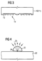
- FIG. 3 essentially corresponds one of the two aforementioned embodiments.
- an annular Recess 16 provided in the coil 14 for generation a magnetic field arranged for magnetic storage is.
- the coil 14 consists, for example, of a evaporated metal layer, which is structured photolithographically is.
- the current for generating the magnetic field in the coil 16 can, for. B. by means of one or more GaAs photodiodes, the on the semiconductor die 10 or on the Carrier plates 11 are applied and for example in operation of the storage device are illuminated with a laser, be provided wirelessly.
- the whole hemispherical lens 20 made of a semiconductor material, the for the electromagnetic used in the storage device Radiation is permeable.
- the wavelength ⁇ that comes from Semiconductor material preferably from the group SiC, GaP, Si, Ge, GaAs.
- the flat surface 21 of the hemispherical lens 20 is preferred with one permeable to radiation 23 of wavelength ⁇ Protective layer is provided, the greater hardness than the semiconductor material and which is optically inactive is (compare this in connection with the figures 1 and 2 exemplary embodiments explained).
- the flat surface 21 of the immersion lens 20 faces during operation of the storage device to the surface of the storage medium 22 such a small distance (e.g. approx. 50 nm) that the medium between immersion lens 20 and storage medium 22, in general Air for the emerging from the immersion lens 20 Radiation with the wavelength ⁇ / n is physically ineffective. For this purpose, this distance is smaller than ⁇ / n6. Between the immersion lens 20 and the storage medium 22 prevail hence physical contact.
- annular Recess 16 is provided in which a coil 14 for Generation of a magnetic field for magnetic storage is arranged.
Landscapes
- Physics & Mathematics (AREA)
- Optics & Photonics (AREA)
- General Physics & Mathematics (AREA)
- Chemical & Material Sciences (AREA)
- Crystallography & Structural Chemistry (AREA)
- Optical Head (AREA)
- Lenses (AREA)
Applications Claiming Priority (2)
| Application Number | Priority Date | Filing Date | Title |
|---|---|---|---|
| DE19738985 | 1997-09-05 | ||
| DE19738985 | 1997-09-05 |
Publications (2)
| Publication Number | Publication Date |
|---|---|
| EP0911653A1 true EP0911653A1 (fr) | 1999-04-28 |
| EP0911653B1 EP0911653B1 (fr) | 2006-07-19 |
Family
ID=7841384
Family Applications (1)
| Application Number | Title | Priority Date | Filing Date |
|---|---|---|---|
| EP98115824A Expired - Lifetime EP0911653B1 (fr) | 1997-09-05 | 1998-08-21 | Système d'immersion |
Country Status (6)
| Country | Link |
|---|---|
| US (1) | US6091694A (fr) |
| EP (1) | EP0911653B1 (fr) |
| JP (1) | JP4109355B2 (fr) |
| KR (1) | KR100433320B1 (fr) |
| DE (1) | DE59813644D1 (fr) |
| TW (1) | TW408324B (fr) |
Cited By (2)
| Publication number | Priority date | Publication date | Assignee | Title |
|---|---|---|---|---|
| WO2001027919A1 (fr) * | 1999-10-15 | 2001-04-19 | Hitachi Maxell, Ltd. | Support d'enregistrement magnéto-optique et enregistreur magnéto-optique |
| EP1054394A3 (fr) * | 1999-05-17 | 2003-02-05 | Samsung Electronics Co. Ltd. | Support d'enregistrement optique pour la réduction de la taille d'une tache optique |
Families Citing this family (26)
| Publication number | Priority date | Publication date | Assignee | Title |
|---|---|---|---|---|
| US6307818B1 (en) * | 1998-06-09 | 2001-10-23 | Seagate Technology Llc | Magneto-optical head with integral mounting of lens holder and coil |
| JP2000113484A (ja) * | 1998-10-07 | 2000-04-21 | Sony Corp | 光学ヘッド用スライダ |
| US6494753B1 (en) | 1999-08-02 | 2002-12-17 | Swenco Products, Inc. | No-crimp electrical connector side-by-side type and method |
| JP2002141556A (ja) | 2000-09-12 | 2002-05-17 | Lumileds Lighting Us Llc | 改良された光抽出効果を有する発光ダイオード |
| US7064355B2 (en) * | 2000-09-12 | 2006-06-20 | Lumileds Lighting U.S., Llc | Light emitting diodes with improved light extraction efficiency |
| US7053419B1 (en) | 2000-09-12 | 2006-05-30 | Lumileds Lighting U.S., Llc | Light emitting diodes with improved light extraction efficiency |
| JP4569800B2 (ja) | 2000-11-22 | 2010-10-27 | ソニー株式会社 | 光学ピックアップ装置及びディスクドライブ装置 |
| WO2002063613A2 (fr) * | 2001-02-07 | 2002-08-15 | University Of Rochester | Systeme et procede d'imagerie optique haute resolution, stockage de donnees, lithographie et controle |
| US6987613B2 (en) | 2001-03-30 | 2006-01-17 | Lumileds Lighting U.S., Llc | Forming an optical element on the surface of a light emitting device for improved light extraction |
| AU2003218274A1 (en) * | 2002-06-28 | 2004-01-19 | Seagate Technology Llc | Heat assisted magnetic recording head with a planar waveguide |
| US7412143B2 (en) * | 2002-06-28 | 2008-08-12 | Seagate Technology Llc | Heat assisted magnetic recording with heat profile shaping |
| AU2003218265A1 (en) * | 2002-06-28 | 2004-01-19 | Seagate Technology Llc | Apparatus and method for producing a small spot of optical energy |
| US7009213B2 (en) * | 2003-07-31 | 2006-03-07 | Lumileds Lighting U.S., Llc | Light emitting devices with improved light extraction efficiency |
| KR101196081B1 (ko) | 2003-11-14 | 2012-11-01 | 에릭 바에르 | 다층 중합체 굴절률 분포형 렌즈 |
| US7272079B2 (en) * | 2004-06-23 | 2007-09-18 | Seagate Technology Llc | Transducer for heat assisted magnetic recording |
| JP2006114196A (ja) * | 2004-09-14 | 2006-04-27 | Sony Corp | ソリッドイマージョンレンズとこれを用いた集光レンズ、光学ピックアップ装置、光記録再生装置及びソリッドイマージョンレンズの形成方法 |
| US20060078031A1 (en) * | 2004-10-08 | 2006-04-13 | Govorkov Sergei V | InGaN LED pumped II-VI semiconductor laser |
| US7304425B2 (en) * | 2004-10-29 | 2007-12-04 | 3M Innovative Properties Company | High brightness LED package with compound optical element(s) |
| US7462502B2 (en) | 2004-11-12 | 2008-12-09 | Philips Lumileds Lighting Company, Llc | Color control by alteration of wavelength converting element |
| US7419839B2 (en) * | 2004-11-12 | 2008-09-02 | Philips Lumileds Lighting Company, Llc | Bonding an optical element to a light emitting device |
| US20060182393A1 (en) * | 2005-02-11 | 2006-08-17 | Seagate Technology Llc | System for confined optical power delivery and enhanced optical transmission efficiency |
| KR100638107B1 (ko) * | 2005-06-09 | 2006-10-24 | 연세대학교 산학협력단 | 이머젼 박막층을 구비하는 광변조 미세개구 어레이 장치 및이를 이용한 고속 미세패턴 기록시스템 |
| US7894308B2 (en) * | 2006-06-27 | 2011-02-22 | Seagate Technology Llc | Near-field optical transducers having a tilted metallic pin |
| US8059354B2 (en) * | 2009-01-29 | 2011-11-15 | Seagate Technology Llc | Transducer for data storage device |
| US8767199B2 (en) | 2010-10-15 | 2014-07-01 | Infrared Laboratories, Inc. | Inspection system utilizing solid immersion lenses |
| EP2867918A1 (fr) * | 2012-06-26 | 2015-05-06 | Kla-Tencor Corporation | Métrologie en champ proche |
Citations (2)
| Publication number | Priority date | Publication date | Assignee | Title |
|---|---|---|---|---|
| GB1491064A (en) * | 1975-05-08 | 1977-11-09 | Mullard Ltd | Composite lenses |
| GB2181567A (en) * | 1985-07-04 | 1987-04-23 | Plessey Co Plc | Infra-red fresnel lenses and methods of fabrication |
Family Cites Families (8)
| Publication number | Priority date | Publication date | Assignee | Title |
|---|---|---|---|---|
| US5121256A (en) * | 1991-03-14 | 1992-06-09 | The Board Of Trustees Of The Leland Stanford Junior University | Lithography system employing a solid immersion lens |
| US5125750A (en) * | 1991-03-14 | 1992-06-30 | The Board Of Trustees Of The Leland Stanford Junior University | Optical recording system employing a solid immersion lens |
| US5497359A (en) * | 1994-08-30 | 1996-03-05 | National Business Machines Corporation | Optical disk data storage system with radiation-transparent air-bearing slider |
| DE19511593C2 (de) * | 1995-03-29 | 1997-02-13 | Siemens Ag | Mikrooptische Vorrichtung |
| JPH08315404A (ja) * | 1995-05-18 | 1996-11-29 | Sony Corp | 光学ピックアップ装置 |
| US5729393A (en) * | 1996-04-03 | 1998-03-17 | Digital Papyrus Corporation | Optical flying head with solid immersion lens having raised central surface facing medium |
| ID16848A (id) * | 1996-05-01 | 1997-11-13 | Terastor Corp | Kepala layang dengan lensa padat yang terbenam |
| US5883872A (en) * | 1997-05-29 | 1999-03-16 | The Board Of Trustees Of The Leland Stanford Junior University | Near field magneto-optical recording system employing slit illumination |
-
1998
- 1998-08-21 EP EP98115824A patent/EP0911653B1/fr not_active Expired - Lifetime
- 1998-08-21 DE DE59813644T patent/DE59813644D1/de not_active Expired - Lifetime
- 1998-08-27 TW TW087114169A patent/TW408324B/zh not_active IP Right Cessation
- 1998-09-03 JP JP24925498A patent/JP4109355B2/ja not_active Expired - Lifetime
- 1998-09-04 KR KR10-1998-0036412A patent/KR100433320B1/ko not_active Expired - Lifetime
- 1998-09-08 US US09/149,814 patent/US6091694A/en not_active Expired - Lifetime
Patent Citations (2)
| Publication number | Priority date | Publication date | Assignee | Title |
|---|---|---|---|---|
| GB1491064A (en) * | 1975-05-08 | 1977-11-09 | Mullard Ltd | Composite lenses |
| GB2181567A (en) * | 1985-07-04 | 1987-04-23 | Plessey Co Plc | Infra-red fresnel lenses and methods of fabrication |
Cited By (2)
| Publication number | Priority date | Publication date | Assignee | Title |
|---|---|---|---|---|
| EP1054394A3 (fr) * | 1999-05-17 | 2003-02-05 | Samsung Electronics Co. Ltd. | Support d'enregistrement optique pour la réduction de la taille d'une tache optique |
| WO2001027919A1 (fr) * | 1999-10-15 | 2001-04-19 | Hitachi Maxell, Ltd. | Support d'enregistrement magnéto-optique et enregistreur magnéto-optique |
Also Published As
| Publication number | Publication date |
|---|---|
| US6091694A (en) | 2000-07-18 |
| TW408324B (en) | 2000-10-11 |
| KR19990029524A (ko) | 1999-04-26 |
| DE59813644D1 (de) | 2006-08-31 |
| KR100433320B1 (ko) | 2004-07-16 |
| JPH11144300A (ja) | 1999-05-28 |
| JP4109355B2 (ja) | 2008-07-02 |
| EP0911653B1 (fr) | 2006-07-19 |
Similar Documents
| Publication | Publication Date | Title |
|---|---|---|
| EP0911653B1 (fr) | Système d'immersion | |
| EP0660467B1 (fr) | Elément optoélectronique et sa méthode de fabrication | |
| DE69600964T2 (de) | Optische Nahfeldvorrichtung mit Laserquelle | |
| DE3536497C2 (fr) | ||
| DE69815860T2 (de) | Integrierter strahlformer und seine verwendung | |
| DE60214186T2 (de) | Verfahren zur Herstellung von optischen Faserkollimatoren im Array | |
| DE69318487T2 (de) | Halbleiterlaservorrichtung, optische Vorrichtung und Herstellungsverfahren | |
| DE68917785T2 (de) | Laserlichtquelle für den sichtbaren Bereich. | |
| EP0873534A2 (fr) | Bloc de composants d'emission optoelectroniques | |
| WO1997004491A1 (fr) | Transducteur optoelectronique et son procede de fabrication | |
| EP0498169A1 (fr) | Composant opto-électronique pour couplage et découplage de rayonnement | |
| DE250824T1 (de) | Integrierter optischer multi-demultiplexer. | |
| DE19621124A1 (de) | Optoelektronischer Wandler und dessen Herstellungsverfahren | |
| DE60017594T2 (de) | Wellenleiter-laser-vorrichtung | |
| DE69227486T2 (de) | Magnetooptischer Lesekopf | |
| EP0076373A2 (fr) | Analyseur de fréquences en technologie des guides d'ondes planaires et méthode pour la construction d'une lentille planaire géodésique sur ou dans un substrat | |
| DE112019002367T5 (de) | Metaflächen-Struktur und Verfahren zum Herstellen einer Metaflächen-Struktur | |
| DE68925809T2 (de) | Optische Wellenlängenkonverter-Einrichtung | |
| EP0815479B1 (fr) | Emetteur-recepteur optique | |
| DE68924193T2 (de) | Erzeugung paralleler, frequenzverdoppelter Strahlen mittels einer optischen Faser. | |
| EP0421118A1 (fr) | Elément de couplage optique avec micro-lentille convexe | |
| DE3421705A1 (de) | Abtastobjektiv mit einem hologramm | |
| EP0367837A2 (fr) | Lentille planconvexe sphérique pour le couplage optique d'un laser semi-conducteur à un guide d'onde | |
| DE69112185T2 (de) | Lichtquelleneinrichtung. | |
| DE112022001742T5 (de) | Monolithisch integrierte optische Baugruppe |
Legal Events
| Date | Code | Title | Description |
|---|---|---|---|
| PUAI | Public reference made under article 153(3) epc to a published international application that has entered the european phase |
Free format text: ORIGINAL CODE: 0009012 |
|
| AK | Designated contracting states |
Kind code of ref document: A1 Designated state(s): DE FR GB |
|
| AX | Request for extension of the european patent |
Free format text: AL;LT;LV;MK;RO;SI |
|
| 17P | Request for examination filed |
Effective date: 19990607 |
|
| AKX | Designation fees paid |
Free format text: DE FR GB |
|
| RAP1 | Party data changed (applicant data changed or rights of an application transferred) |
Owner name: INFINEON TECHNOLOGIES AG |
|
| 17Q | First examination report despatched |
Effective date: 20030318 |
|
| RAP1 | Party data changed (applicant data changed or rights of an application transferred) |
Owner name: OSRAM OPTO SEMICONDUCTORS GMBH |
|
| GRAP | Despatch of communication of intention to grant a patent |
Free format text: ORIGINAL CODE: EPIDOSNIGR1 |
|
| GRAS | Grant fee paid |
Free format text: ORIGINAL CODE: EPIDOSNIGR3 |
|
| GRAA | (expected) grant |
Free format text: ORIGINAL CODE: 0009210 |
|
| AK | Designated contracting states |
Kind code of ref document: B1 Designated state(s): DE FR GB |
|
| PG25 | Lapsed in a contracting state [announced via postgrant information from national office to epo] |
Ref country code: GB Free format text: LAPSE BECAUSE OF FAILURE TO SUBMIT A TRANSLATION OF THE DESCRIPTION OR TO PAY THE FEE WITHIN THE PRESCRIBED TIME-LIMIT Effective date: 20060719 |
|
| REG | Reference to a national code |
Ref country code: GB Ref legal event code: FG4D Free format text: NOT ENGLISH |
|
| REF | Corresponds to: |
Ref document number: 59813644 Country of ref document: DE Date of ref document: 20060831 Kind code of ref document: P |
|
| GBV | Gb: ep patent (uk) treated as always having been void in accordance with gb section 77(7)/1977 [no translation filed] |
Effective date: 20060719 |
|
| EN | Fr: translation not filed | ||
| PLBE | No opposition filed within time limit |
Free format text: ORIGINAL CODE: 0009261 |
|
| STAA | Information on the status of an ep patent application or granted ep patent |
Free format text: STATUS: NO OPPOSITION FILED WITHIN TIME LIMIT |
|
| 26N | No opposition filed |
Effective date: 20070420 |
|
| PG25 | Lapsed in a contracting state [announced via postgrant information from national office to epo] |
Ref country code: FR Free format text: LAPSE BECAUSE OF FAILURE TO SUBMIT A TRANSLATION OF THE DESCRIPTION OR TO PAY THE FEE WITHIN THE PRESCRIBED TIME-LIMIT Effective date: 20070511 |
|
| PG25 | Lapsed in a contracting state [announced via postgrant information from national office to epo] |
Ref country code: FR Free format text: LAPSE BECAUSE OF FAILURE TO SUBMIT A TRANSLATION OF THE DESCRIPTION OR TO PAY THE FEE WITHIN THE PRESCRIBED TIME-LIMIT Effective date: 20060719 |
|
| PGFP | Annual fee paid to national office [announced via postgrant information from national office to epo] |
Ref country code: DE Payment date: 20170822 Year of fee payment: 20 |
|
| REG | Reference to a national code |
Ref country code: DE Ref legal event code: R071 Ref document number: 59813644 Country of ref document: DE |