EP0911872A2 - Verfahren zur Herstellung von Dünnschichttransistoren - Google Patents
Verfahren zur Herstellung von Dünnschichttransistoren Download PDFInfo
- Publication number
- EP0911872A2 EP0911872A2 EP98119277A EP98119277A EP0911872A2 EP 0911872 A2 EP0911872 A2 EP 0911872A2 EP 98119277 A EP98119277 A EP 98119277A EP 98119277 A EP98119277 A EP 98119277A EP 0911872 A2 EP0911872 A2 EP 0911872A2
- Authority
- EP
- European Patent Office
- Prior art keywords
- layer
- amorphous silicon
- electrically conductive
- structuring
- conductive layer
- Prior art date
- Legal status (The legal status is an assumption and is not a legal conclusion. Google has not performed a legal analysis and makes no representation as to the accuracy of the status listed.)
- Withdrawn
Links
Images
Classifications
-
- H—ELECTRICITY
- H10—SEMICONDUCTOR DEVICES; ELECTRIC SOLID-STATE DEVICES NOT OTHERWISE PROVIDED FOR
- H10D—INORGANIC ELECTRIC SEMICONDUCTOR DEVICES
- H10D30/00—Field-effect transistors [FET]
- H10D30/01—Manufacture or treatment
- H10D30/021—Manufacture or treatment of FETs having insulated gates [IGFET]
- H10D30/031—Manufacture or treatment of FETs having insulated gates [IGFET] of thin-film transistors [TFT]
- H10D30/0312—Manufacture or treatment of FETs having insulated gates [IGFET] of thin-film transistors [TFT] characterised by the gate electrodes
- H10D30/0316—Manufacture or treatment of FETs having insulated gates [IGFET] of thin-film transistors [TFT] characterised by the gate electrodes of lateral bottom-gate TFTs comprising only a single gate
-
- H—ELECTRICITY
- H10—SEMICONDUCTOR DEVICES; ELECTRIC SOLID-STATE DEVICES NOT OTHERWISE PROVIDED FOR
- H10P—GENERIC PROCESSES OR APPARATUS FOR THE MANUFACTURE OR TREATMENT OF DEVICES COVERED BY CLASS H10
- H10P30/00—Ion implantation into wafers, substrates or parts of devices
- H10P30/20—Ion implantation into wafers, substrates or parts of devices into semiconductor materials, e.g. for doping
- H10P30/202—Ion implantation into wafers, substrates or parts of devices into semiconductor materials, e.g. for doping characterised by the semiconductor materials
- H10P30/204—Ion implantation into wafers, substrates or parts of devices into semiconductor materials, e.g. for doping characterised by the semiconductor materials into Group IV semiconductors
-
- H—ELECTRICITY
- H10—SEMICONDUCTOR DEVICES; ELECTRIC SOLID-STATE DEVICES NOT OTHERWISE PROVIDED FOR
- H10D—INORGANIC ELECTRIC SEMICONDUCTOR DEVICES
- H10D30/00—Field-effect transistors [FET]
- H10D30/01—Manufacture or treatment
- H10D30/021—Manufacture or treatment of FETs having insulated gates [IGFET]
- H10D30/031—Manufacture or treatment of FETs having insulated gates [IGFET] of thin-film transistors [TFT]
- H10D30/0321—Manufacture or treatment of FETs having insulated gates [IGFET] of thin-film transistors [TFT] comprising silicon, e.g. amorphous silicon or polysilicon
-
- H—ELECTRICITY
- H10—SEMICONDUCTOR DEVICES; ELECTRIC SOLID-STATE DEVICES NOT OTHERWISE PROVIDED FOR
- H10D—INORGANIC ELECTRIC SEMICONDUCTOR DEVICES
- H10D30/00—Field-effect transistors [FET]
- H10D30/60—Insulated-gate field-effect transistors [IGFET]
- H10D30/67—Thin-film transistors [TFT]
- H10D30/6704—Thin-film transistors [TFT] having supplementary regions or layers in the thin films or in the insulated bulk substrates for controlling properties of the device
- H10D30/6713—Thin-film transistors [TFT] having supplementary regions or layers in the thin films or in the insulated bulk substrates for controlling properties of the device characterised by the properties of the source or drain regions, e.g. compositions or sectional shapes
-
- H—ELECTRICITY
- H10—SEMICONDUCTOR DEVICES; ELECTRIC SOLID-STATE DEVICES NOT OTHERWISE PROVIDED FOR
- H10D—INORGANIC ELECTRIC SEMICONDUCTOR DEVICES
- H10D30/00—Field-effect transistors [FET]
- H10D30/60—Insulated-gate field-effect transistors [IGFET]
- H10D30/67—Thin-film transistors [TFT]
- H10D30/6729—Thin-film transistors [TFT] characterised by the electrodes
- H10D30/673—Thin-film transistors [TFT] characterised by the electrodes characterised by the shapes, relative sizes or dispositions of the gate electrodes
- H10D30/6732—Bottom-gate only TFTs
-
- H—ELECTRICITY
- H10—SEMICONDUCTOR DEVICES; ELECTRIC SOLID-STATE DEVICES NOT OTHERWISE PROVIDED FOR
- H10P—GENERIC PROCESSES OR APPARATUS FOR THE MANUFACTURE OR TREATMENT OF DEVICES COVERED BY CLASS H10
- H10P30/00—Ion implantation into wafers, substrates or parts of devices
- H10P30/20—Ion implantation into wafers, substrates or parts of devices into semiconductor materials, e.g. for doping
- H10P30/21—Ion implantation into wafers, substrates or parts of devices into semiconductor materials, e.g. for doping of electrically active species
- H10P30/212—Through-implantation
Definitions
- the invention relates to a method for producing thin-film transistors with amorphous silicon as a semiconductor material.
- etching stopper process Another process in which doped amorphous silicon for the drain and source contacts are deposited, the so-called "etching stopper process".
- a metal layer is first deposited as a gate contact and structured.
- a PECVD system successively a gate insulator, amorphous silicon as well deposited an etch stop layer and then the etch stop layer structured in a mask process.
- the surface oxide that has formed over the structure removed before doped amorphous silicon is deposited.
- Another is then deposited and structured Metal layer for the drain and source connections.
- the metal layer together with the etch stop layer serves as a mask in the subsequent structuring of the doped and undoped Silicon layers.
- the etch stop layer acts as an implant protection for the semiconductor channel.
- Another metal layer for the drain and source connections is then deposited and structured.
- the metal layer then serves together with the structured etch stop layer as a mask for structuring the doped amorphous silicon layer.
- the electrical contact to the metallic drain and source connections arranged above is relatively poor.
- This problem can only be avoided by etching away part of the surface of the doped silicon layer.
- this etching step also has poor reproducibility. This method is therefore not a standard process for the production of thin-film transistors.
- the present invention is based on the object Process for the production of thin film transistors with to create amorphous silicon as a semiconductor, which has the disadvantages avoids the known methods.
- the method according to the invention is therefore characterized in that that the ion implantation by the second electrically conductive Layer occurs through. This makes it possible Maximum of the ion concentration at the interface of the semiconductor layer to place the electrically conductive layer. The ohmic contact between the second electrically conductive Layer and the doped semiconductor layer is thereby very good.
- the semiconductor layer can be chosen to be very thin, which is an improvement in the properties of the transistors, especially with regard to low light sensitivity and lower reverse currents.
- the oxidation of the semiconductor surface does not interfere with this method, so that the surface oxide does not need to be removed. Thereby the reproducibility of the process is also very high, which makes there is a constant high yield of error-free transistors can be achieved.
- the transistors very good electrical properties in terms of mobility, Threshold voltage and reverse current.
- the electrical resistance can occur after ion beam implantation also applied another electrically conductive layer become.
- phosphorus atoms can be in the amorphous Silicon layer are implanted.
- silicon nitride can preferably be applied as the etching stop layer become. Then the deposition of the gate insulator, of the amorphous silicon and the etch stop layer without Interrupt the vacuum in a PECVD system.
- the electrically conductive layers can be expediently Use metals.
- the invention also includes a thin film transistor which is produced by a method according to the invention and an amorphous silicon layer doped by ion implantation having.
- the maximum of the doping distribution in the silicon layer preferably on the surface of the layer lie.
- Thin-film transistors are the control of the pixels of a liquid crystal display.
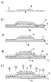
- Step a) shows the deposition of a conductive layer 10 on a glass substrate 11 and the structuring of this layer 10 as the gate G of the transistor.
- step b) a gate insulator 12, amorphous silicon 13 and an etch stop layer 14 are successively deposited on the layer 10 in a PECVD process, the gate insulator and the etch stop layer preferably being made of silicon nitride.
- the structuring of the etching stop layer 14 is shown in step c).
- the ion beam implantation may preferably with an energy of 20 - 30 keV and a dose of about 1E15 cm 3 - 1E16 cm 3 done.
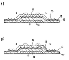
- the second electrically conductive layer 15 is structured as a drain and source D, S in step f).
- the doped amorphous silicon layer 13 is structured with the etch stop layer 14 and the electrically conductive layer 15 as a mask, and the transistor is thus completed.
Landscapes
- Thin Film Transistor (AREA)
Abstract
Description
- Aufbringen einer ersten elektrisch leitfähigen Schicht auf ein Substrat und Strukturieren als Gate-Kontakt des Transistors,
- Aufbringen eines Gate-Isolators,
- Aufbringen von amorphem Silizium,
- Aufbringen und Strukturieren einer Ätzstoppschicht,
- Aufbringen einer zweiten elektrisch leitfähigen Schicht für die Drain- und Source-Anschlüsse,
- Ionenstrahlimplantation durch die zweite elektrisch leitfähige Schicht hindurch in die amorphe Siliziumschicht mit der Ätzstoppschicht als Implantierschutzschicht für den Halbleiterkanal,
- Strukturieren der zweiten elektrisch leitfähigen Schicht als Drain- und Source-Kontakte,
- Strukturieren der implantierten amorphen Siliziumschicht mit der zweiten elektrisch leitfähigen Schicht und der Ätzstoppschicht als Maske.
Claims (9)
- Verfahren zur Herstellung von Dünnschichttransistoren mit amorphem Silizium als Halbleitermaterial, gekennzeichnet durch die Prozeßschritte:Aufbringen einer ersten elektrisch leitfähigen Schicht (10) auf ein Substrat (11) und Strukturieren als Gate-Kontakt (G) des Transistors,Aufbringen eines Gate-Isolators (12),Aufbringen von amorphem Silizium (13),Aufbringen und Strukturieren einer Ätzstoppschicht (14),Aufbringen einer zweiten elektrisch leitfähigen Schicht (15) für die Drain- und Source-Anschlüsse (D, S),Ionenstrahlimplantation durch die zweite elektrisch leitfähige Schicht (15) hindurch in die amorphe Siliziumschicht (13) mit der Ätzstoppschicht (14) als Implantierschutzschicht für den Halbleiterkanal,Strukturieren der zweiten elektrisch leitfähigen Schicht (15) als Drain- und Source-Kontakte (D, S),Strukturieren der implantierten amorphen Siliziumschicht (13) mit der zweiten elektrisch leitfähigen Schicht (15) und der Ätzstoppschicht (14) als Maske.
- Verfahren nach Anspruch 1, dadurch gekennzeichnet, daß nach der Ionenstrahlimplantation eine weitere elektrisch leitfähige Schicht zur Erniedrigung des elektrischen Widerstands aufgebracht wird.
- Verfahren nach Anspruch 1 oder 2, dadurch gekennzeichnet, daß Phosphor-Atome in die amorphe Siliziumschicht (13) implantiert werden.
- Verfahren nach einem der Ansprüche 1 bis 3, dadurch gekennzeichnet, daß als Gate-Isolator (12) Siliziumnitrid aufgebracht wird.
- Verfahren nach einem der Ansprüche 1 bis 4, dadurch gekennzeichnet, daß als Ätzstoppschicht (14) Siliziumnitrid aufgebracht wird.
- Verfahren nach einem der Ansprüche 1 bis 5, dadurch gekennzeichnet, daß die Abscheidung des Gate-Isolators (12), des amorphen Siliziums (13) und der Ätzstoppschicht (14) ohne Unterbrechung des Vakuums in einem PECVD-System erfolgt.
- Verfahren nach einem der Ansprüche 1 bis 6, dadurch gekennzeichnet, daß für die elektrisch leitfähigen Schichten (10, 15) Metalle aufgebracht werden.
- Dünnschichttransistor, hergestellt nach einem der Verfahren der Ansprüche 1 bis 6, mit einer durch Ionenimplantation dotierten amorphen Siliziumschicht (13).
- Dünnschichttransistor nach Anspruch 8, dadurch gekennzeichnet, daß das Maximum der Dotierungsverteilung in der Siliziumschicht (13) an der Oberfläche der Schicht liegt.
Applications Claiming Priority (2)
| Application Number | Priority Date | Filing Date | Title |
|---|---|---|---|
| DE19746961A DE19746961C2 (de) | 1997-10-24 | 1997-10-24 | Verfahren zur Herstellung von Dünnschichttransistoren |
| DE19746961 | 1997-10-24 |
Publications (2)
| Publication Number | Publication Date |
|---|---|
| EP0911872A2 true EP0911872A2 (de) | 1999-04-28 |
| EP0911872A3 EP0911872A3 (de) | 1999-11-17 |
Family
ID=7846462
Family Applications (1)
| Application Number | Title | Priority Date | Filing Date |
|---|---|---|---|
| EP98119277A Withdrawn EP0911872A3 (de) | 1997-10-24 | 1998-10-13 | Verfahren zur Herstellung von Dünnschichttransistoren |
Country Status (5)
| Country | Link |
|---|---|
| EP (1) | EP0911872A3 (de) |
| KR (1) | KR19990037326A (de) |
| CA (1) | CA2251438A1 (de) |
| DE (1) | DE19746961C2 (de) |
| TW (1) | TW400585B (de) |
Cited By (1)
| Publication number | Priority date | Publication date | Assignee | Title |
|---|---|---|---|---|
| WO2001015234A1 (en) * | 1999-08-24 | 2001-03-01 | Koninklijke Philips Electronics N.V. | Thin-film transistors and method for producing the same |
Families Citing this family (1)
| Publication number | Priority date | Publication date | Assignee | Title |
|---|---|---|---|---|
| KR100865257B1 (ko) * | 2002-09-16 | 2008-10-24 | 엘지디스플레이 주식회사 | 액정표시장치용 박막트랜지스터의 제조방법 |
Family Cites Families (6)
| Publication number | Priority date | Publication date | Assignee | Title |
|---|---|---|---|---|
| US4339869A (en) * | 1980-09-15 | 1982-07-20 | General Electric Company | Method of making low resistance contacts in semiconductor devices by ion induced silicides |
| EP0493113B1 (de) * | 1990-12-28 | 1997-03-19 | Sharp Kabushiki Kaisha | Ein Verfahren zum Herstellen eines Dünnfilm-Transistors und eines Aktive-Matrix-Substrates für Flüssig-Kristall-Anzeige-Anordnungen |
| JPH05283427A (ja) * | 1991-02-18 | 1993-10-29 | Hitachi Ltd | 薄膜トランジスタの製造方法及びそれを用いたアクテブマトリックス型液晶表示装置 |
| FR2690074B1 (fr) * | 1992-04-15 | 1999-06-11 | Louis Beaud | Elements gonflables pour matelas anti-escarres. |
| JP2949404B2 (ja) * | 1993-05-20 | 1999-09-13 | エルジイ・セミコン・カンパニイ・リミテッド | 薄膜トランジスタ及びその製造方法 |
| JPH07211915A (ja) * | 1994-01-20 | 1995-08-11 | Casio Comput Co Ltd | 薄膜トランジスタの製造方法 |
-
1997
- 1997-10-24 DE DE19746961A patent/DE19746961C2/de not_active Expired - Fee Related
-
1998
- 1998-10-13 EP EP98119277A patent/EP0911872A3/de not_active Withdrawn
- 1998-10-21 TW TW087117372A patent/TW400585B/zh active
- 1998-10-22 CA CA002251438A patent/CA2251438A1/en not_active Abandoned
- 1998-10-23 KR KR1019980044492A patent/KR19990037326A/ko not_active Withdrawn
Cited By (3)
| Publication number | Priority date | Publication date | Assignee | Title |
|---|---|---|---|---|
| WO2001015234A1 (en) * | 1999-08-24 | 2001-03-01 | Koninklijke Philips Electronics N.V. | Thin-film transistors and method for producing the same |
| US6403408B1 (en) | 1999-08-24 | 2002-06-11 | U.S. Philips Corporation | Thin-film transistors and method for producing the same |
| US6504182B2 (en) | 1999-08-24 | 2003-01-07 | Koninklijke Philips Electronics N.V. | Thin-film transistors |
Also Published As
| Publication number | Publication date |
|---|---|
| CA2251438A1 (en) | 1999-04-24 |
| KR19990037326A (ko) | 1999-05-25 |
| EP0911872A3 (de) | 1999-11-17 |
| TW400585B (en) | 2000-08-01 |
| DE19746961A1 (de) | 1999-05-06 |
| DE19746961C2 (de) | 1999-08-12 |
Similar Documents
| Publication | Publication Date | Title |
|---|---|---|
| DE3688758T2 (de) | Dünnfilmtransistor auf isolierendem Substrat. | |
| DE68912482T2 (de) | Dünnfilm-Transistoren, ihre Verfahren zur Herstellung und Anzeigeeinrichtung, die mit solchen Transistoren hergestellt sind. | |
| DE69209678T2 (de) | Halbleiteranordnung für Hochspannungsverwendung und Verfahren zur Herstellung | |
| DE69434643T2 (de) | Struktur und Herstellung von Leistungs-MOSFET unter Einbeziehung der Struktur des Randes | |
| DE69734643T2 (de) | Elektronische einrichtung mit nitrid-chrom enthaltenden elektroden und verfahren zur herstellung | |
| DE69435045T2 (de) | Halbleiter-Anordnung und Herstellungsverfahren dafür | |
| DE69212383T2 (de) | Dünnfilmtransistor und Verfahren zu seiner Herstellung | |
| DE60132994T2 (de) | Verfahren zur herstellung eines leistungs-mosfets | |
| DE68921567T2 (de) | Flüssigkristallanzeigetafel mit verminderten Pixeldefekten. | |
| DE19654738B4 (de) | Verfahren zum Herstellen einer Halbleitervorrichtung | |
| DE3939319C2 (de) | Verfahren zum Herstellen eines asymmetrischen Feldeffekttransistors | |
| DE60219300T2 (de) | Halbleiteranordnungen mit graben-gateelektrode und verfahren zu deren herstellung | |
| EP0001574B1 (de) | Halbleiteranordnung für Widerstandsstrukturen in hochintegrierten Schaltkreisen und Verfahren zur Herstellung dieser Halbleiteranordnung | |
| DE3618000A1 (de) | Verfahren zur herstellung von transistoren auf einem siliziumsubstrat | |
| DE3601326A1 (de) | Halbleiter, insbesondere hochspannungs-mos-feldeffekt-halbleiter | |
| DE3714164A1 (de) | Fluessigkristallanzeige | |
| DE3603470A1 (de) | Verfahren zur herstellung von feldeffektbauelementen auf einem siliziumsubstrat | |
| DE3887447T2 (de) | Flüssigkristall-Anzeigevorrichtung. | |
| DE3788470T2 (de) | Verfahren zur Herstellung eines Feldeffekttransistors mit isoliertem Gate. | |
| EP0012220A1 (de) | Verfahren zur Herstellung eines Schottky-Kontakts mit selbstjustierter Schutzringzone | |
| DE2262943A1 (de) | Verfahren zur verhinderung einer unerwuenschten inversion | |
| DE3540422C2 (de) | Verfahren zum Herstellen integrierter Strukturen mit nicht-flüchtigen Speicherzellen, die selbst-ausgerichtete Siliciumschichten und dazugehörige Transistoren aufweisen | |
| DE2922016A1 (de) | Vlsi-schaltungen | |
| DE4130555A1 (de) | Halbleitervorrichtung mit hoher durchbruchsspannung und geringem widerstand, sowie herstellungsverfahren | |
| DE69131376T2 (de) | Verfahren zur Herstellung von doppelt-diffundierten integrierten MOSFET-Zellen |
Legal Events
| Date | Code | Title | Description |
|---|---|---|---|
| PUAI | Public reference made under article 153(3) epc to a published international application that has entered the european phase |
Free format text: ORIGINAL CODE: 0009012 |
|
| AK | Designated contracting states |
Kind code of ref document: A2 Designated state(s): FR GB NL |
|
| AX | Request for extension of the european patent |
Free format text: AL;LT;LV;MK;RO;SI |
|
| PUAL | Search report despatched |
Free format text: ORIGINAL CODE: 0009013 |
|
| RIC1 | Information provided on ipc code assigned before grant |
Free format text: 6H 01L 21/336 A, 6H 01L 21/265 B |
|
| AK | Designated contracting states |
Kind code of ref document: A3 Designated state(s): AT BE CH CY DE DK ES FI FR GB GR IE IT LI LU MC NL PT SE |
|
| AX | Request for extension of the european patent |
Free format text: AL;LT;LV;MK;RO;SI |
|
| 17P | Request for examination filed |
Effective date: 20000428 |
|
| AKX | Designation fees paid |
Free format text: FR GB NL |
|
| REG | Reference to a national code |
Ref country code: DE Ref legal event code: 8566 |
|
| RAP1 | Party data changed (applicant data changed or rights of an application transferred) |
Owner name: UNIVERSITAET STUTTGART |
|
| STAA | Information on the status of an ep patent application or granted ep patent |
Free format text: STATUS: THE APPLICATION IS DEEMED TO BE WITHDRAWN |
|
| 18D | Application deemed to be withdrawn |
Effective date: 20040502 |