EP0911906B1 - Structure d'antenne plane transparente - Google Patents
Structure d'antenne plane transparente Download PDFInfo
- Publication number
- EP0911906B1 EP0911906B1 EP19980119520 EP98119520A EP0911906B1 EP 0911906 B1 EP0911906 B1 EP 0911906B1 EP 19980119520 EP19980119520 EP 19980119520 EP 98119520 A EP98119520 A EP 98119520A EP 0911906 B1 EP0911906 B1 EP 0911906B1
- Authority
- EP
- European Patent Office
- Prior art keywords
- transparent
- transparent planar
- antenna
- thin film
- radiating element
- Prior art date
- Legal status (The legal status is an assumption and is not a legal conclusion. Google has not performed a legal analysis and makes no representation as to the accuracy of the status listed.)
- Expired - Lifetime
Links
- 229910052751 metal Inorganic materials 0.000 claims description 87
- 239000002184 metal Substances 0.000 claims description 87
- 239000010409 thin film Substances 0.000 claims description 64
- 239000010408 film Substances 0.000 claims description 53
- 238000004891 communication Methods 0.000 claims description 48
- 239000000463 material Substances 0.000 claims description 21
- 230000000007 visual effect Effects 0.000 claims description 19
- PXHVJJICTQNCMI-UHFFFAOYSA-N Nickel Chemical compound [Ni] PXHVJJICTQNCMI-UHFFFAOYSA-N 0.000 claims description 6
- 239000004697 Polyetherimide Substances 0.000 claims description 6
- BASFCYQUMIYNBI-UHFFFAOYSA-N platinum Chemical compound [Pt] BASFCYQUMIYNBI-UHFFFAOYSA-N 0.000 claims description 6
- 229920001601 polyetherimide Polymers 0.000 claims description 6
- -1 polyethylene Polymers 0.000 claims description 6
- RYGMFSIKBFXOCR-UHFFFAOYSA-N Copper Chemical compound [Cu] RYGMFSIKBFXOCR-UHFFFAOYSA-N 0.000 claims description 5
- 229910052802 copper Inorganic materials 0.000 claims description 5
- 239000010949 copper Substances 0.000 claims description 5
- 239000011521 glass Substances 0.000 claims description 5
- 229910052735 hafnium Inorganic materials 0.000 claims description 4
- 229910052738 indium Inorganic materials 0.000 claims description 4
- AMGQUBHHOARCQH-UHFFFAOYSA-N indium;oxotin Chemical compound [In].[Sn]=O AMGQUBHHOARCQH-UHFFFAOYSA-N 0.000 claims description 4
- 239000004973 liquid crystal related substance Substances 0.000 claims description 4
- 239000004417 polycarbonate Substances 0.000 claims description 4
- 229910052710 silicon Inorganic materials 0.000 claims description 4
- 229910052715 tantalum Inorganic materials 0.000 claims description 4
- 229910052718 tin Inorganic materials 0.000 claims description 4
- 239000011135 tin Substances 0.000 claims description 4
- 229910052719 titanium Inorganic materials 0.000 claims description 4
- 239000010936 titanium Substances 0.000 claims description 4
- 229910052726 zirconium Inorganic materials 0.000 claims description 4
- VYZAMTAEIAYCRO-UHFFFAOYSA-N Chromium Chemical compound [Cr] VYZAMTAEIAYCRO-UHFFFAOYSA-N 0.000 claims description 3
- FYYHWMGAXLPEAU-UHFFFAOYSA-N Magnesium Chemical compound [Mg] FYYHWMGAXLPEAU-UHFFFAOYSA-N 0.000 claims description 3
- ZOKXTWBITQBERF-UHFFFAOYSA-N Molybdenum Chemical compound [Mo] ZOKXTWBITQBERF-UHFFFAOYSA-N 0.000 claims description 3
- 239000004698 Polyethylene Substances 0.000 claims description 3
- 239000004642 Polyimide Substances 0.000 claims description 3
- XUIMIQQOPSSXEZ-UHFFFAOYSA-N Silicon Chemical compound [Si] XUIMIQQOPSSXEZ-UHFFFAOYSA-N 0.000 claims description 3
- BQCADISMDOOEFD-UHFFFAOYSA-N Silver Chemical compound [Ag] BQCADISMDOOEFD-UHFFFAOYSA-N 0.000 claims description 3
- ATJFFYVFTNAWJD-UHFFFAOYSA-N Tin Chemical compound [Sn] ATJFFYVFTNAWJD-UHFFFAOYSA-N 0.000 claims description 3
- RTAQQCXQSZGOHL-UHFFFAOYSA-N Titanium Chemical compound [Ti] RTAQQCXQSZGOHL-UHFFFAOYSA-N 0.000 claims description 3
- QCWXUUIWCKQGHC-UHFFFAOYSA-N Zirconium Chemical compound [Zr] QCWXUUIWCKQGHC-UHFFFAOYSA-N 0.000 claims description 3
- NIXOWILDQLNWCW-UHFFFAOYSA-N acrylic acid group Chemical group C(C=C)(=O)O NIXOWILDQLNWCW-UHFFFAOYSA-N 0.000 claims description 3
- 229910045601 alloy Inorganic materials 0.000 claims description 3
- 239000000956 alloy Substances 0.000 claims description 3
- 229910052782 aluminium Inorganic materials 0.000 claims description 3
- XAGFODPZIPBFFR-UHFFFAOYSA-N aluminium Chemical compound [Al] XAGFODPZIPBFFR-UHFFFAOYSA-N 0.000 claims description 3
- 229910052804 chromium Inorganic materials 0.000 claims description 3
- 239000011651 chromium Substances 0.000 claims description 3
- 229910017052 cobalt Inorganic materials 0.000 claims description 3
- 239000010941 cobalt Substances 0.000 claims description 3
- GUTLYIVDDKVIGB-UHFFFAOYSA-N cobalt atom Chemical compound [Co] GUTLYIVDDKVIGB-UHFFFAOYSA-N 0.000 claims description 3
- PCHJSUWPFVWCPO-UHFFFAOYSA-N gold Chemical compound [Au] PCHJSUWPFVWCPO-UHFFFAOYSA-N 0.000 claims description 3
- 229910052737 gold Inorganic materials 0.000 claims description 3
- 239000010931 gold Substances 0.000 claims description 3
- VBJZVLUMGGDVMO-UHFFFAOYSA-N hafnium atom Chemical compound [Hf] VBJZVLUMGGDVMO-UHFFFAOYSA-N 0.000 claims description 3
- APFVFJFRJDLVQX-UHFFFAOYSA-N indium atom Chemical compound [In] APFVFJFRJDLVQX-UHFFFAOYSA-N 0.000 claims description 3
- 229910052749 magnesium Inorganic materials 0.000 claims description 3
- 239000011777 magnesium Substances 0.000 claims description 3
- WPBNNNQJVZRUHP-UHFFFAOYSA-L manganese(2+);methyl n-[[2-(methoxycarbonylcarbamothioylamino)phenyl]carbamothioyl]carbamate;n-[2-(sulfidocarbothioylamino)ethyl]carbamodithioate Chemical compound [Mn+2].[S-]C(=S)NCCNC([S-])=S.COC(=O)NC(=S)NC1=CC=CC=C1NC(=S)NC(=O)OC WPBNNNQJVZRUHP-UHFFFAOYSA-L 0.000 claims description 3
- 229910052750 molybdenum Inorganic materials 0.000 claims description 3
- 239000011733 molybdenum Substances 0.000 claims description 3
- 229910052759 nickel Inorganic materials 0.000 claims description 3
- 229910052758 niobium Inorganic materials 0.000 claims description 3
- 239000010955 niobium Substances 0.000 claims description 3
- GUCVJGMIXFAOAE-UHFFFAOYSA-N niobium atom Chemical compound [Nb] GUCVJGMIXFAOAE-UHFFFAOYSA-N 0.000 claims description 3
- 229910052697 platinum Inorganic materials 0.000 claims description 3
- 229920000515 polycarbonate Polymers 0.000 claims description 3
- 229920000573 polyethylene Polymers 0.000 claims description 3
- 229920001721 polyimide Polymers 0.000 claims description 3
- 239000004810 polytetrafluoroethylene Substances 0.000 claims description 3
- 229920001343 polytetrafluoroethylene Polymers 0.000 claims description 3
- 239000010703 silicon Substances 0.000 claims description 3
- 229910052709 silver Inorganic materials 0.000 claims description 3
- 239000004332 silver Substances 0.000 claims description 3
- GUVRBAGPIYLISA-UHFFFAOYSA-N tantalum atom Chemical compound [Ta] GUVRBAGPIYLISA-UHFFFAOYSA-N 0.000 claims description 3
- WFKWXMTUELFFGS-UHFFFAOYSA-N tungsten Chemical compound [W] WFKWXMTUELFFGS-UHFFFAOYSA-N 0.000 claims description 3
- 229910052721 tungsten Inorganic materials 0.000 claims description 3
- 239000010937 tungsten Substances 0.000 claims description 3
- 229910052720 vanadium Inorganic materials 0.000 claims description 3
- LEONUFNNVUYDNQ-UHFFFAOYSA-N vanadium atom Chemical compound [V] LEONUFNNVUYDNQ-UHFFFAOYSA-N 0.000 claims description 3
- RHZWSUVWRRXEJF-UHFFFAOYSA-N indium tin Chemical compound [In].[Sn] RHZWSUVWRRXEJF-UHFFFAOYSA-N 0.000 claims description 2
- XOLBLPGZBRYERU-UHFFFAOYSA-N tin dioxide Chemical compound O=[Sn]=O XOLBLPGZBRYERU-UHFFFAOYSA-N 0.000 claims description 2
- 229910001887 tin oxide Inorganic materials 0.000 claims description 2
- 238000013461 design Methods 0.000 description 10
- 239000004020 conductor Substances 0.000 description 6
- 238000005516 engineering process Methods 0.000 description 3
- 230000005855 radiation Effects 0.000 description 3
- 230000004044 response Effects 0.000 description 3
- 238000010586 diagram Methods 0.000 description 2
- 239000003989 dielectric material Substances 0.000 description 2
- 230000009931 harmful effect Effects 0.000 description 2
- 238000004519 manufacturing process Methods 0.000 description 2
- 239000007769 metal material Substances 0.000 description 2
- 238000000034 method Methods 0.000 description 2
- 230000008569 process Effects 0.000 description 2
- 230000004888 barrier function Effects 0.000 description 1
- 230000001413 cellular effect Effects 0.000 description 1
- 230000001010 compromised effect Effects 0.000 description 1
- 238000010276 construction Methods 0.000 description 1
- 230000001419 dependent effect Effects 0.000 description 1
- 238000000151 deposition Methods 0.000 description 1
- 238000009792 diffusion process Methods 0.000 description 1
- 238000005530 etching Methods 0.000 description 1
- 230000036541 health Effects 0.000 description 1
- 238000010438 heat treatment Methods 0.000 description 1
- 210000003734 kidney Anatomy 0.000 description 1
- 239000011159 matrix material Substances 0.000 description 1
- 150000002739 metals Chemical class 0.000 description 1
- 230000003287 optical effect Effects 0.000 description 1
- 230000003071 parasitic effect Effects 0.000 description 1
- 238000012545 processing Methods 0.000 description 1
- 230000001681 protective effect Effects 0.000 description 1
- 230000009467 reduction Effects 0.000 description 1
- 230000003678 scratch resistant effect Effects 0.000 description 1
- 238000000926 separation method Methods 0.000 description 1
- 238000012546 transfer Methods 0.000 description 1
Images




Classifications
-
- H—ELECTRICITY
- H01—ELECTRIC ELEMENTS
- H01Q—ANTENNAS, i.e. RADIO AERIALS
- H01Q9/00—Electrically-short antennas having dimensions not more than twice the operating wavelength and consisting of conductive active radiating elements
- H01Q9/04—Resonant antennas
- H01Q9/0407—Substantially flat resonant element parallel to ground plane, e.g. patch antenna
- H01Q9/045—Substantially flat resonant element parallel to ground plane, e.g. patch antenna with particular feeding means
-
- H—ELECTRICITY
- H01—ELECTRIC ELEMENTS
- H01Q—ANTENNAS, i.e. RADIO AERIALS
- H01Q9/00—Electrically-short antennas having dimensions not more than twice the operating wavelength and consisting of conductive active radiating elements
- H01Q9/04—Resonant antennas
- H01Q9/0407—Substantially flat resonant element parallel to ground plane, e.g. patch antenna
Definitions
- the present invention relates generally to a portable wireless communications device and, more particularly, to a transparent planar antenna structure overlying the device's liquid crystal display (LCD).
- LCD liquid crystal display
- wireless communications devices continues to shrink, as the use for such devices expands in both well established, and new communication technologies. These communication technologies include pagers, telephones, televisions, GPS and other satellite receivers, and wireless LAN.
- communication technologies include pagers, telephones, televisions, GPS and other satellite receivers, and wireless LAN.
- One of the key elements in the performance of a wireless unit is the unit's antenna.
- the antenna size is a limiting factor in further reducing the size of wireless devices.
- Whip type antennas are relatively large, and recently, concerns have surfaced regarding the harmful effects of an omni-directional radiation of hand-held transmitters. Further, the whip antenna extends from the chassis and is easily damaged.
- Antennas can be incorporated into, or on the device chassis.
- One obvious choice of antenna is the so-called patch design. As the name suggests this antenna is built as a thin sheet that can be layered over an existing structure.
- Fig. 13 illustrates the coplanar layout of a panel antenna 10 (prior art).
- the design of such antennas is well known to consist of a conductive radiating element 12 surrounded by a conductive ground plane 14.
- the panel antenna 10 can be fabricated, for example, on a PC board with the conductor being a thin film of copper overlying a sheet of dielectric material.
- the radiating element 12 is patterned to be electrically isolated from the ground plane 14.
- the radiating element 12 and the ground plane 14 are isolated by etching through the copper until a portion 16 of the underlying dielectric material, represented by cross-hatched lines, is exposed.
- Fig. 14 is a partial cross-sectional view of the panel antenna 10 of Fig. 13 (prior art).
- the radiating element 12 and the ground plane 14 (conductive regions), overlying dielectric layer 18, are represented with cross-hatched lines.
- the design of an antenna for a coplanar arrangement of the radiating element 12 (radiator) and the ground plane 14 is based on well understood relationships such as the separation between ground planes (b), conductor width (a), the dielectric constant ( ⁇ r ) of the dielectric layer 18, thickness (t) of the ground plane 14 (radiator), the thickness (h) of the dielectric layer 18, and the effective wavelength of the intended resonant frequency.
- the design of a cellular telephone illustrates the difficulties of antenna design.
- half of the surface area of the phone is occupied with user-operated switches, such as a keypad, and an electronic display for viewing.
- the keypad and LCD display are co-located on the same "side" of the phone so that the operator can see the results of keypad manipulations. It is difficult to locate an antenna on this user-interface side of the telephone.
- Consumer preference for larger displays and improvements in technology increasing the size of LCDs act to further limit the area available for the placement of conventional or patch antennas.
- EP-A-0 331 201 discloses an amorphous oxide film and articles having such a film thereon.
- the amorphous oxide film is essentially composed of an oxide containing at least one member selected from the group consisting of Zr, Ti, Hf, Sn, Ta and In and at least one member selected from the group consisting of B and Si.
- articles comprising said amorphous oxide film this document describes surface-coated mirrors, low-reflective glass, heat radiation shielding glass, metal diffusion barrier layers, scratch-resistant protective film provided on a transparent sheet and the like. This document does not describe to use the amorphous oxide film for providing a transparent planar antenna.
- an antenna could be placed on a chassis in the area of the user-operated functions. Specifically, it would be advantageous if an antenna could be designed to co-exist with the relatively large, planar surface of the visual display panel.
- the present invention comprises a transparent antenna, comprising a first transparent sheet of thin film and a first transparent planar radiating element having a first operating frequency and overlying said first transparent sheet of thin film, whereby structures underlying said first transparent sheet of thin film are visible, and a first transparent planar ground plane, characterized in that said transparent planar radiating element and said first transparent planar ground plane include highly conductive metal film structures selected from the group consisting of a grid of parallel oriented metal lines and a mesh of orthogonal and parallel oriented metal lines.
- the present invention further comprises a wireless communication's device which includes a flat panel electronic visual display and at least a first transparent planar antenna having a construction mentioned immediately before, wherein said first transparent planar antenna is located overlying said flat panel electronic visual display.
- the first antenna includes the radiating element and ground plane being located coplanar overlying the first transparent sheet of thin film.
- the thin film is selected from the group of materials consisting of polyethylene telephthalate (PET), polyethylesulfone (PES), polyetherimide (PEI), polycarbonate, polyimide, polytetrafluoroethylene, acrylic, glass, and combinations of the above mentioned materials.
- the first antenna radiator (first transparent planar radiating element) and the ground plane include a metal film structure overlying the first thin film patterned to electrically isolate the radiator from the ground plane.
- the metal film structure is selected from the group consisting of a grid of parallel oriented metal lines and a mesh of orthogonal and parallel oriented metal lines.
- the material of the metal film structure is selected from the group of materials consisting of copper, aluminum, gold, silver, nickel, chromium, titanium, molybdenum, tin, tantalum, magnesium, cobalt, platinum, tungsten, manganese, silicon, zirconium, vanadium, niobium, hafnium, indium and other alloys of the above mentioned materials.
- the grid-like structure of the conductors permit the first antenna to be greater than 65 percent transmissive in the band of visible light wavelengths.
- a second transparent antenna having a second operating frequency has a radiating element located coplanar to the first transparent planar radiating element.
- the first and second antenna radiating elements are located coplanar to a shared ground plane.
- the second antenna has a radiating element located on a second thin film, overlying the first thin film, and the first and second antenna radiating elements share the first transparent planar ground plane.
- the second transparent antenna operates either at the same frequency as the first antenna, or at a different frequency.
- Another alternate design includes a first transparent sheet of thin film on which the first radiating element is mounted, and a second transparent sheet of thin film, underlying the first transparent sheet of thin film, on which the first transparent planar ground plane is mounted.
- the antenna is located in two sheets of overlying thin film.
- the radiating element is a planar rectangle, or oval shape, as is typical in the design of patch antennas.
- the radiating elements are configured inter-digitally using either a grid of parallel oriented metal lines, or a mesh of orthogonal and parallel oriented metal lines.
- a wireless device having a plurality of receivers and transmitters, each operatively connected to an independent transparent antenna, is also provided.
- the transparent antennas are as described above.
- the low cost and low profile of the transparent antennas permit each radio frequency (RF) section of the wireless device to have its own antenna, unlike many prior art wireless devices where RF sections must share a single antenna. In this manner, the necessity of a duplexer circuit is eliminated.
- RF radio frequency
- Fig. 1 is a cross-sectional view of the transparent panel antenna section of a wireless communications device 30.
- the wireless communications device 30 comprises a flat panel electronic visual display 32.
- the flat panel electronic visual display 32 is a liquid crystal display (LCD).
- the wireless communications device 30 also comprises at least a first transparent planar antenna 34, having a first operating frequency, a highly conductive planar radiating element 36, and a highly conductive first transparent planar ground plane 38.
- the first transparent planar antenna 34 overlies the flat panel electronic visual display 32 so that the display 32 is viewed through the first transparent planar antenna 34.
- Fig. 2 illustrates, in greater detail, the first transparent planar antenna 34 of Fig. 1.
- the wireless communications device 30 further comprises a first transparent sheet of thin film 40.
- the first transparent planar antenna 34 includes the first transparent planar radiating element 36 and the first transparent planar ground plane 38 being located coplanar and overlying the first transparent sheet of thin film 40, whereby the first transparent planar antenna 34 is located on the single transparent sheet of thin film 40.
- the first transparent planar radiating element 36 and the first transparent planar ground plane 38 are mounted under the first transparent sheet of thin film 40, so that the first transparent sheet of thin film 40 overlies the first transparent planar radiating element 36, the first transparent planar ground plane 38, and the flat panel electronic visual display 32.
- the first transparent sheet of thin film 40 is selected from the group of materials consisting of polyethylene telephthalate (PET), polyethylesulfone (PES), polyetherimide (PEI), polycarbonate, polyimide, polytetrafluoroethylene, acrylic, glass, and combinations of the above mentioned materials.
- the first transparent sheet of thin film 40 has a thickness t 42 in the range between 100 and 400 microns.
- the first transparent planar radiating element 36 and the first transparent planar ground plane 38 include a metal film structure 44 overlying the first transparent sheet of thin film 40 patterned to electrically isolate the first transparent planar radiating element 36 (radiator) from the first transparent planar ground plane 38, whereby the metal permits high electrical conductivity in the first transparent planar antenna 34.
- the metal film structure 44 is fabricated by depositing a sheet of the metal film material overlying the first transparent sheet of thin film 40. Then, the metal film structure 44 is etched with a variety of processes that are well known in the art of integrated circuit (IC) processing, such as using a patterned photo-resist profile as an etch mask.
- IC integrated circuit
- the metal film structure 44 is selected from the group consisting of a grid of parallel oriented metal lines and a mesh of orthogonal and parallel oriented metal lines.
- Fig. 3 illustrates the grid metal film structure 44.
- the conductive lines appear as parallel bars.
- Fig. 4 illustrates the mesh metal film structure 44.
- the conductive lines appear as a screen.
- the material of the metal film structure 44 is selected from the group of materials consisting of copper, aluminum, gold, silver, nickel, chromium, titanium, molybdenum, tin, tantalum, magnesium, cobalt, platinum, tungsten, manganese, silicon, zirconium, vanadium, niobium, hafnium, indium and other alloys of the above mentioned materials.
- Fig. 5 is a microscope picture illustrating a detailed section of the grid of Fig. 3.
- the metal lines have a width in the range between 1 and 30 microns ( ⁇ m). Specifically, Fig. 5 shows a line width of 10 microns.
- the parallel oriented metal lines are separated by a distance, or gap in the range between 30 microns and 1 mm. Specifically, Fig. 5 shows a gap of 40 microns.
- the gap between conductive lines is calculated in response to the operating, or resonant first frequency of the first transparent planar antenna 34. In some cases, the gap is chosen, at least partially, in response to pitch, or the spacing between electrical elements of underlying LCD 32 (not shown).
- each metal line of the metal film structure 44 so as to correspond to a pixel pitch of the flat panel electric visual display 32 (the metal lines which are the non-transparent section of the metal film structure are formed in the non-display area between pixels of the flat panel display section), an improved visibility of the flat panel display section can be achieved.
- the non-display area between adjacent pixels of the flat panel electric visual display 32 indicates, for example, a space between pixel electrodes of the liquid crystal display, where a black matrix is formed.
- the gap is chosen to be no greater than one-tenth of the effective first wavelength.
- the effective wavelength is calculated in response to the thickness t 46 of the metal film structure 44, and the dielectric constant ( ⁇ r ) and thickness t 42 of the first transparent sheet of thin film 40 (Fig. 2). Because the above-mentioned metal materials are good conductors, and the shape of the metal film structure 44 insures good conductivity, the metal film structure 44 remains very conductive when the metal film thickness t 46 is thin.
- the metal film thickness t 46 is in the range between 300 and 100,000 ⁇ .
- the line widths and gaps forming the metal film structure 44 are also shaped to provide optical transparency.
- the minimum gap which provides transparency is approximately 30 microns, which is about the width of 1 pixel in an LCD, and the minimum line width is approximately 1 micron.
- line widths and gaps between lines are chosen so that the first transparent planar antenna 34 is greater than 65 percent transmissive in the band of visible light wavelengths.
- the gap between parallel and intersecting lines varies from a square shape to a rectangular shape.
- the square shape has gap dimensions from 30 microns to 1 mm between the parallel lines oriented in a first direction.
- the gap between one set of parallel lines differs from the gap between the set of parallel lines oriented orthogonal to the first direction so that a rectangle is formed.
- the present invention is not limited to any particular pattern of metal lines, although regularly placed lines and gaps are easier to fabricate.
- the key feature of the present invention is that the metal film structure 44 be both highly conductive and transparent.
- the metal film structure 44 is selected from the group of materials consisting of indium-tin, indium-tin oxide, and tin oxide. These materials are not as conductive as the metal, named above. Therefore, the thickness t 46 (Fig. 2) must be greater to provide equivalent conductance to the metals. Then, the metal film structure 44 has a metal film thickness t 46 in the range between 0.1 and 10 microns.
- the wireless communications device 30 further comprises a second transparent planar antenna 50 having a second operating frequency, different than the first operating frequency.
- the second transparent planar antenna 50 has a second transparent planar radiating element 52 located coplanar to the first transparent antenna radiating element 36.
- the first and second transparent planar radiating elements 36, 52 are located coplanar to a shared first transparent planar ground plane 38.
- the second transparent planar antenna 50 has an operating frequency the same as the first operating frequency.
- the second transparent planar antenna 50 has the second transparent planar radiating element 52 located coplanar to the first transparent antenna radiating element 36, and the first and second transparent planar radiating elements 36, 52 are located coplanar to the shared first transparent planar ground plane 38.
- the wireless communications device 30 further comprises a plurality of transparent antennas, including at least third and fourth transparent planar antennas 54 and 56. It can be seen from Fig. 6 that the size of the metal film structure 44 is variable to provide enough space for several antennas. For simplicity, only four antennas are shown.
- Each of the plurality of transparent planar antennas 50, 54, and 56 have a transparent planar radiating element (52, 58 and 60) located coplanar to the first transparent antenna radiating element 36.
- the plurality of transparent planar radiating elements 36, 52, 58 and 60 are located coplanar to the first transparent planar ground plane 38.
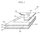
- Fig. 7 illustrates a plurality of non-coplanar transparent antennas.
- the wireless communications device 30 further comprises a second transparent sheet of thin film 62 overlying the first transparent sheet of thin film 40.
- the wireless communications device 30 also comprises a second transparent planar antenna 50 having a second operating frequency different than the first operating frequency.
- the second transparent planar antenna 50 has the second transparent planar radiating element 52 located overlying the second transparent sheet of thin film 62.
- the first and second transparent planar radiating elements 36 and 52 share the first transparent planar ground plane 38.
- the second transparent planar antenna 50 has an operating frequency the same as the first operating frequency.
- the wireless communications device 30 further comprises a plurality of sheets of thin film overlying the first transparent sheet of thin film 40, and a plurality of transparent antennas having a plurality of corresponding radiating elements.
- Each one of the plurality of transparent planar radiating elements overlies a corresponding one of the plurality of sheets of thin film, and each radiating element shares the first transparent planar ground plane 38.
- a third transparent planar antenna 54 including a third transparent sheet of thin film 70 and a third transparent planar radiating element 58, are shown in Fig. 7. However, it can be seen that additional antennas are stackable overlying the third transparent planar antenna 54.
- a cross-section of the third transparent planar antenna 54 is shown removed to provide a clear view of the second transparent planar antenna 50.
- Fig. 8 illustrates a touch panel in use with the present invention.
- the wireless communications device 30 further comprises a transparent user-activated touch panel 74 overlying the flat panel electronic visual display 32.
- touch panels such as touch panel 74, overlying computer screens and electronic displays is a well known computer interface for use either without, or in addition to, a keypad.
- the touch panel 74 including user-activated sensors 75 corresponding to visual prompts represented on the flat panel electronic visual display 32 visible through the first transparent planar antenna 34 and the transparent touch panel 74.
- the thin film materials and thicknesses of the touch panel 74 are similar to the first transparent sheet of thin film 40 of the first transparent planar antenna 34.
- the touch panel 74 is placed between the first transparent planar antenna 34 and the flat panel electronic visual display 32.
- the transparent touch panel 74 and the first transparent planar antenna 34 are both mounted on the first transparent sheet of thin film 40.
- the first transparent planar antenna 34 and the touch panel 74 are fabricated on the same transparent sheet of thin film 40 with the conductive regions of the first transparent planar antenna 34 and the touch panel 74 on opposite sides of the first transparent sheet of thin film 40.
- Fig. 9 illustrates a non-coplanar embodiment of the present invention.
- the wireless communications device 30 comprises a fourth transparent sheet of the thin film 76 on which the first transparent radiating element 36 is mounted, and a fifth transparent sheet of thin film 78, underlying the fourth transparent sheet of thin film 76, on which the first transparent planar ground plane 38 is mounted.
- the first transparent planar antenna 34 is located on two sheets of overlying sheets of thin film 76 and 78.
- Fig. 10 depicts an inter-digital antenna embodiment of the transparent antenna of the present invention.
- the wireless communications device 30 of Fig. 1 further comprises a second transparent planar antenna 50 having a second operating frequency.
- the second transparent planar radiating element 52 is located coplanar to the first transparent antenna radiating element 36.
- the first and second transparent planar radiating elements 36 and 52 are co-located in the inter-digital metal film structure 44.
- the first and second transparent planar antennas 34 and 50 are located with a coplanar ground plane (not shown, see Fig. 1). Alternately, the ground is on a different plane (not shown, see Fig. 9) from the transparent planar radiating elements (36, 52).
- the spacing between the digits of the first and second transparent planar radiating elements 36 and 52 is dependent are the operating frequencies of the first and second transparent planar antennas 34 and 50, the effective wavelengths, and the mutual parasitic effects of antennas being closely located.
- Fig. 10 is not drawn to scale. The digits, as drawn, appear visible with respect to the overall panel only for the purpose of showing the alternating digits of the first and second transparent planar antennas 34 and 50. Since the grid and mesh line widths and gaps are actually on the order of microns, they are not typically visible to the human eye.
- the inter-digital metal structure 44 is selected from the group consisting of a grid of parallel oriented lines and a mesh of orthogonal and parallel oriented metal lines.
- the metal lines have a width in the range between 1 and 30 microns, with a spacing between parallel oriented metal lines in the range between 30 microns and 1 mm.
- the space between lines or sections of mesh include the digits of another antenna.
- a mesh version of the second transparent planar radiating element 52 is shown in Section A, and the grid versions of the transparent planar radiating elements 36 and 52 are shown in Section B of Fig. 10.
- Fig. 11 illustrates non-conductive, or dummy sections of grid and mesh metal structures 80 in use with the first transparent planar antenna 34 of the present invention.
- the non-conductive metal film structure 80 overlies the first transparent sheet of thin film 40 (not shown) and is patterned to be an electrical isolator.
- the non-conductive metal film structure 80 is selected from the group consisting of a grid of parallel oriented non-conductive metal lines and a mesh of orthogonal and parallel oriented non-conductive metal lines.
- the non-conductive grid, Section A of Fig. 11, and the non-conductive mesh, Section B of Fig. 11, are similar to the conductive grid and mesh metal structures 44, discussed above and shown in Figs. 3, 4 and 5. However, there are breaks in the grid and mesh patterns so that they do not conduct electrically.
- the non-conductive grid and mesh structures 80 are used in the same antenna as conductive grid and mesh structures 44 to normalize transparency. That is, to make the transparency through the non-conductive areas surrounding the first transparent radiating element 36 and the first transparent planar ground plane 38 the same as the first transparent planar radiating element 36 and the first transparent planar ground plane 38.
- Fig. 12 is a schematic block diagram of the wireless communications device 30 communicating information at a plurality of frequencies.
- the wireless communications device 30 comprises at least a first receiver 90 (first communicating section) having an input operatively connected to a line 92 to receive information at a first operating frequency.
- the wireless communications device 30 further comprises at least a second receiver 94 (second communicating section) having an input operatively connected to a line 96 to receive information at a second operating frequency, different than the first operating frequency.
- the wireless communications device 30 comprises the first transparent planar antenna 34 including a highly conductive first transparent planar radiating element 36 and the first transparent planar ground plane 38, as described above and shown in Figs. 1-5 and 8-11.
- the first transparent planar antenna 34 is operatively connected to the first receiver 90 without any operative connection to the second receiver 94.
- the wireless communications device 30 comprises the second transparent planar antenna 50 as described above and shown in Figs. 6 and 7.
- the second transparent planar antenna 50 includes the highly conductive second transparent planar radiating element 52 and the first transparent planar ground plane 38.
- the first transparent planar ground plane 38 is coplanar with the second transparent planar radiating element 52 as shown in Fig. 6. Alternately, the first transparent planar ground plane 38 is on a different plane than the second transparent planar radiating element 52, as shown in Fig. 7.
- the second transparent planar antenna 50 is operatively connected to the second receiver 94 without any operative connection to the first receiver 90.
- the first and second transparent planar radiating elements 36 and 52 and the first transparent planar ground plane 38 are the metal film structures 44 selected from the group consisting of a grid of parallel oriented metal lines and a mesh of orthogonal and parallel oriented metal lines, as described above and shown in Figs. 3-5.
- the use of two antennas eliminates the need for a duplexer circuit as is needed in many wireless communications devices to de-couple multiple receivers when they share only one antenna.
- the second receiver 94 is replaced with at least a transmitter 98 (second communicating section) having a second operating frequency, different than the first operating frequency.
- the second operating frequency is the same as the first operating frequency.
- the wireless communications device 30 has separate antennas, the first transparent planar antenna 34 operatively connected to the first receiver 90, and the second transparent planar antenna 50 operatively connected to the transmitter 98.
- the use of two antennas eliminates the need for a duplexer circuit. Because of the low cost and low profile of the present invention transparent antenna, the wireless communications device 30 is able to provide a separate antenna for each radio frequency section of the communications device without the use of either duplexers or antenna switches.
- the use of independent transparent antennas for each of a plurality of receiver and transmitter sections is also an application of the present invention.
- additional circuitry such as amplifiers and filters interface between the first and second transparent planar antennas 34 and 50, and receivers 90 and 94, and transmitter 98, as is well known in the art.
- additional circuitry such as amplifiers and filters interface between the first and second transparent planar antennas 34 and 50, and receivers 90 and 94, and transmitter 98, as is well known in the art.
- the above mentioned devices must be interfaced with conductive lines having precisely defined impedances.
- the conductive lines interfacing the first and second transparent planar radiating elements 36 and 52 are transparent when mounted on the thin film, and fabricated with conductive grid and mesh metal structures 44.
- amplifiers, filters, and other circuit components are mounted on thin film, even though these elements are not transparent.
- the non-transparent structures are placed where visibility of underlying the flat panel electronic visual display 32 is not critical.
- the present invention allows one of the largest surface areas of a wireless communications device, the flat panel LCD, to be used for a second purpose, as a surface to mount an antenna.
- the fabrication of an antenna from thin films of conductive material on a transparent thin film permits the antenna of the present invention to have the performance characteristics of prior art patch antennas, while being transparent enough to allow the user to view the display through the antenna.
- the small profile of the transparent antennas makes it relatively easy to design an antenna system of transparent panel antennas with a summing network to add the direction gain of several antennas, yielding an omni-directional antennas gain pattern.
- the use of just a single transparent antenna, providing essentially hemispherical coverage, to minimize RF output in the direction of the wireless device user, is desirable when RF emissions are a health concern.
- Other embodiments of the present invention will occur to those skilled in the art.
Landscapes
- Support Of Aerials (AREA)
- Details Of Aerials (AREA)
- Waveguide Aerials (AREA)
Claims (28)
- Antenne transparente, comprenant:- une première feuille transparente de film mince (40); et- un premier élément rayonnant plan transparent (36) présentant une première fréquence de fonctionnement et recouvrant ladite première feuille transparente de film mince (40), les structures sous-jacentes à ladite feuille transparente de film mince (40) étant de ce fait visibles; et- un premier plan de masse plan transparent (38),
caractérisée en ce que ledit élément rayonnant plan transparent (36) et ledit premier plan de masse plan transparent (38) comprennent des structures de film métallique hautement conductrices (44) sélectionnées parmi le groupe composé d'une grille de lignes métalliques orientées parallèlement et d'une trame de lignes métalliques orientées parallèlement et orthogonalement. - Antenne transparente selon la revendication 1, caractérisée en ce que ledit premier plan de masse plan transparent (38) recouvre ladite première feuille transparente de film mince (40), ledit premier élément rayonnant plan transparent (36) et ledit premier plan de masse plan transparent (38) étant de ce fait situés dans le même plan l'un et l'autre.
- Antenne transparente selon la revendication 1 ou 2, caractérisée en ce que ladite première feuille transparente de film mince (40) a une épaisseur dans la gamme comprise entre 100 et 400 µm.
- Antenne transparente selon la revendication 1, caractérisée en ce qu'elle comprend en outre une deuxième feuille transparente de film mince (62) recouvrant ladite première feuille transparente de film mince (40), dans laquelle ledit premier plan de masse plan transparent (38) est monté sur ladite deuxième feuille transparente de film mince (62), la première antenne plane transparente (34) étant de ce fait située sur deux feuilles transparentes de films minces superposés (40, 62).
- Antenne transparente selon la revendication 1, caractérisée en ce que lesdites structures de films métalliques (44) sont sélectionnées parmi le groupe de matières composé du cuivre, de l'aluminium, de l'or, de l'argent, du nickel, du chrome, du titane, du molybdène, de l'étain, du magnésium, du cobalt, du platine, du tungstène, du manganèse, du silicium, du zirconium, du vanadium, du niobium, du hafnium, de l'indium et d'autres alliages des matières mentionnées ci-dessus.
- Antenne transparente selon la revendication 1 ou 5, caractérisée en ce que lesdites lignes métalliques ont une largeur dans la gamme comprise entre 1 et 30 µm, et dans laquelle des lignes métalliques orientées parallèlement sont séparées par une distance dans la gamme comprise entre 30 µm et 1 mm.
- Antenne transparente selon l'une quelconque des revendications 1 à 6, caractérisée en ce que lesdites structures de films métalliques (44) recouvrant ladite première feuille transparente de film mince (40) ont une épaisseur de film métallique dans la gamme comprise entre 0,03 µm et 10 µm.
- Antenne transparente selon la revendication 1, caractérisée en ce que la matière desdites structures de films métalliques (44) est sélectionnée parmi le groupe de matières composé de indium-étain, indium-oxyde d'étain, oxyde d'étain, et dans laquelle ledit film métallique a une épaisseur de film métallique dans la gamme comprise entre 0,1 et 10 µm.
- Antenne transparente selon l'une quelconque des revendications 1 à 8, caractérisée en ce que l'antenne transparente est transmissive à plus de 65 % dans la bande des longueurs d'onde de la lumière visible.
- Antenne transparente selon la revendication 2, caractérisée en ce qu'elle comprend en outre un deuxième élément rayonnant plan transparent (52), dans laquelle ledit deuxième élément rayonnant plan transparent (52) est situé dans le même plan que ledit premier élément rayonnant plan transparent (38), lesdits premier et deuxième éléments rayonnants plans transparents (38, 52) étant de ce fait coplanaires audit premier plan de masse plan transparent (38).
- Antenne transparente selon la revendication 2, caractérisée en ce qu'elle comprend en outre une pluralité d'éléments rayonnants plans transparents (52, 58, 60), dans laquelle ladite pluralité d'éléments rayonnants plans transparents (52, 58, 60) est située dans le même plan que ledit premier élément rayonnant plan transparent (36) et que ledit premier plan de masse plan transparent (38).
- Appareil de communication sans fil qui comprend un écran d'affichage électronique plat (32) et au moins une antenne plane transparente (34) selon l'une quelconque des revendications 1 à 9, dans lequel ladite antenne plane transparente (34) est située en recouvrement dudit écran d'affichage électronique plat (32).
- Appareil de communication sans fil selon la revendication 12, caractérisé en ce que ladite première feuille transparente de film mince (40) est sélectionnée parmi le groupe de matières composé de polyéthylène téréphtalate (PET), polyéthylesulfone (PES), polyétherimide (PEI), polycarbonate, polyimide, polytétrafluoroéthylène, acrylique, verre, et des combinaisons des matières mentionnées ci-dessus.
- Appareil de communication sans fil selon la revendication 12 ou 13, caractérisé en ce qu'il comprend en outre une section factice d'une structure de film métallique non conductrice (80) ayant la même transparence que celle de ladite structure de film métallique (44), dans lequel ladite section factice (80) comprend les mêmes lignes métalliques que la pluralité de lignes métalliques de ladite structure de film métallique (44), et ladite section factice (80) comprend une structure de film non conductrice en coupant une partie de chacune desdites lignes métalliques.
- Appareil de communication sans fil selon l'une quelconque des revendications 12 à 14, caractérisé en ce que ledit écran d'affichage électronique plat (32) est un écran d'affichage à cristaux liquides (LCD).
- Appareil de communication sans fil selon la revendication 12, caractérisé en ce qu'il comprend en outre une deuxième antenne plane transparente (50) présentant une deuxième fréquence de fonctionnement, différente de la première fréquence de fonctionnement, dans lequel ladite deuxième antenne plane transparente (50) comporte un deuxième élément rayonnant plan transparent situé dans le même plan que ledit premier élément rayonnant plan transparent (36), et dans lequel lesdits premier et deuxième éléments rayonnants plans transparents (36, 52) sont coplanaires au premier plan de masse plan transparent partagé (38).
- Appareil de communication sans fil selon la revendication 12, caractérisé en ce qu'il comprend en outre une deuxième antenne plane transparente (50) présentant une deuxième fréquence de fonctionnement, identique à la première fréquence de fonctionnement, dans lequel ladite deuxième antenne plane transparente (50) comporte un deuxième élément rayonnant plan transparent (52) situé dans le même plan que ledit premier élément rayonnant plan transparent (36), et dans lequel lesdits premier et deuxième éléments rayonnants plans transparents (36, 52) sont coplanaires au premier plan de masse plan transparent partagé (38).
- Appareil de communication sans fil selon la revendication 12, comprenant en outre une deuxième feuille transparente de film mince (62) recouvrant ladite première feuille transparente de film mince (40), et une deuxième antenne plane transparente (50) présentant une deuxième fréquence de fonctionnement, différente de la première fréquence de fonctionnement, dans lequel ladite deuxième antenne plane transparente (50) comporte un deuxième élément rayonnant plan transparent (52) situé en recouvrement de ladite deuxième feuille transparente de film mince (62), et dans lequel lesdits premier et deuxième éléments rayonnants plans transparents (36, 52) partagent ledit premier plan de masse plan transparent (38).
- Appareil de communication sans fil selon la revendication 12, caractérisé en ce qu'il comprend en outre une deuxième feuille transparente de film mince (62) recouvrant ladite première feuille transparente de film mince (40), et une deuxième antenne plane transparente (50) présentant une deuxième fréquence de fonctionnement, identique à la première fréquence de fonctionnement, dans lequel ladite deuxième antenne plane transparente (50) comporte un premier élément rayonnant plan transparent (52) recouvrant ladite deuxième feuille transparente de film mince (62) et ledit premier élément rayonnant plan transparent (36) et ledit deuxième élément rayonnant plan transparent (52) partagent ledit premier plan de masse plan transparent (38).
- Appareil de communication sans fil selon la revendication 12, caractérisé en ce qu'il comprend en outre une pluralité d'antennes planes transparentes (50, 54, 56), dans lequel ladite pluralité d'antennes ont chacune un élément rayonnant plan transparent (52, 58, 60) situé dans le même plan que ledit premier élément rayonnant plan transparent (36), et dans lequel chacun de ladite pluralité d'éléments rayonnants plans transparents (52, 58, 60) est coplanaire audit premier plan de masse plan transparent (38).
- Appareil de communication sans fil selon la revendication 12, caractérisé en ce qu'il comprend en outre une pluralité de feuilles transparentes de film mince (62, 70) d'une structure stratifiée, une pluralité d'antennes planes transparentes (50, 54, 60), ladite pluralité d'antennes planes transparentes comportant des éléments rayonnants plans transparents (52, 58 et 60) respectivement, et partageant ledit premier plan de masse plan transparent (38), et ladite pluralité d'antennes planes transparentes (50, 54, 56), chacun de ladite pluralité d'éléments rayonnants plans transparents (52, 58, 60) recouvrant une feuille correspondante de ladite pluralité de feuilles de film mince (62, 70, 76).
- Appareil de communication sans fil selon la revendication 12, caractérisé en ce qu'il comprend en outre un panneau tactile transparent (74), activé par l'utilisateur, recouvrant ledit écran d'affichage électronique plan (32), ledit panneau tactile transparent activé par l'utilisateur comportant des capteurs (75) activés par l'utilisateur, correspondant à des guides visuels affichés sur ledit écran d'affichage électronique plan visibles à travers ladite première antenne transparente (34) et ledit panneau tactile transparent (74).
- Appareil de communication sans fil selon la revendication 22, caractérisé en ce que ledit panneau tactile transparent (74) et ladite première antenne plane transparente (34) sont tous les deux montés sur ladite première feuille transparente de film mince (40).
- Appareil de communication sans fil selon la revendication 12, caractérisé en ce qu'il comprend en outre une deuxième antenne plane transparente (50) présentant une deuxième fréquence de fonctionnement, ledit deuxième élément rayonnant plan transparent (52) étant situé dans le même plan que ledit premier élément rayonnant plan transparent (36), dans lequel lesdits premier et deuxième éléments rayonnants plans transparents (36, 38) sont situés conjointement dans une structure de film métallique interdigitée (44), dans lequel ladite structure de film métallique interdigitée (44) est sélectionnée parmi le groupe composé d'une grille de lignes métalliques orientées parallèlement et d'une trame de lignes métalliques orientées parallèlement et orthogonalement, et dans lequel lesdites lignes métalliques ont une largeur dans la gamme comprise entre 1 et 30 µm avec un écartement entre des lignes métalliques orientées parallèlement dans la gamme comprise entre 30 µm et 1 mm.
- Appareil de communication sans fil selon la revendication 12 ou 24, caractérisé en ce que chaque ligne métallique de ladite structure de film métallique (44) est formée dans une zone sans affichage entre des pixels dudit écran d'affichage électronique plan (32).
- Appareil de communication sans fil selon la revendication 14, caractérisé en ce qu'il comprend en outre une première section de communication (90) pour communiquer des informations à la première fréquence de fonctionnement, une deuxième section de communication (94, 98) pour communiquer des informations à la deuxième fréquence de fonctionnement, dans lequel ladite première antenne plane transparente (34) est connectée de façon opérationnelle à ladite première section de communication (90) sans aucune connexion opérationnelle à ladite deuxième section de communication (94, 98), et ladite deuxième antenne plane transparente (50) est connectée de façon opérationnelle à ladite deuxième section de communication (94, 98) sans aucune connexion opérationnelle à ladite première section de communication (90), l'utilisation des deux antennes planes transparentes (34, 50) éliminant de ce fait la nécessité d'un circuit de duplexeur.
- Appareil de communication sans fil selon la revendication 26, caractérisé en ce que ladite première section de communication (90) est une première section de réception (90) pourvue d'une section d'entrée pour recevoir des informations à la première fréquence de fonctionnement, et ladite deuxième section de communication (94, 98) est une deuxième section de réception (94) pourvue d'une section d'entrée pour recevoir des informations à la deuxième fréquence de fonctionnement.
- Appareil de communication sans fil selon la revendication 26, caractérisé en ce que ladite première section de communication (90) est une section de réception (90) pourvue d'une section d'entrée pour recevoir des informations à la première fréquence de fonctionnement, et ladite deuxième section de communication (94, 98) est une section de transmission (98) pourvue d'une section de sortie (98) pour transmettre des informations à la deuxième fréquence de fonctionnement.
Applications Claiming Priority (2)
| Application Number | Priority Date | Filing Date | Title |
|---|---|---|---|
| US953251 | 1992-09-30 | ||
| US95325197A | 1997-10-17 | 1997-10-17 |
Publications (3)
| Publication Number | Publication Date |
|---|---|
| EP0911906A2 EP0911906A2 (fr) | 1999-04-28 |
| EP0911906A3 EP0911906A3 (fr) | 2000-12-06 |
| EP0911906B1 true EP0911906B1 (fr) | 2006-03-08 |
Family
ID=25493750
Family Applications (1)
| Application Number | Title | Priority Date | Filing Date |
|---|---|---|---|
| EP19980119520 Expired - Lifetime EP0911906B1 (fr) | 1997-10-17 | 1998-10-15 | Structure d'antenne plane transparente |
Country Status (3)
| Country | Link |
|---|---|
| EP (1) | EP0911906B1 (fr) |
| JP (1) | JP3490304B2 (fr) |
| DE (1) | DE69833716T2 (fr) |
Cited By (7)
| Publication number | Priority date | Publication date | Assignee | Title |
|---|---|---|---|---|
| US20120050222A1 (en) * | 2010-09-01 | 2012-03-01 | Tsuyoshi Magami | Touch Sensor And Fluorescent Display Having The Same |
| WO2017201197A1 (fr) * | 2016-05-20 | 2017-11-23 | Kymeta Corporation | Testeur de segments d'espace libre (fsst) |
| US10416826B2 (en) | 2012-07-11 | 2019-09-17 | Dai Nippon Printing Co., Ltd. | Touch panel sensor, touch panel device and display device |
| US10461428B2 (en) | 2018-02-23 | 2019-10-29 | Qualcomm Incorporated | Multi-layer antenna |
| US11133596B2 (en) | 2018-09-28 | 2021-09-28 | Qualcomm Incorporated | Antenna with gradient-index metamaterial |
| EP3346354B1 (fr) * | 2015-10-05 | 2022-03-09 | Samsung Electronics Co., Ltd. | Dispositif électronique possédant une unité d'affichage ayant une pluralité de zones |
| US12311637B2 (en) | 2022-11-04 | 2025-05-27 | Agc Automotive Americas Co. | Laminated glazing assembly including an antenna assembly |
Families Citing this family (68)
| Publication number | Priority date | Publication date | Assignee | Title |
|---|---|---|---|---|
| US6621410B1 (en) * | 1996-08-26 | 2003-09-16 | Rf Code, Inc. | System for item and orientation identification |
| US6388621B1 (en) * | 2000-06-20 | 2002-05-14 | Harris Corporation | Optically transparent phase array antenna |
| DE10135951A1 (de) * | 2001-07-24 | 2003-02-20 | Siemens Ag | Mobilfunk-Endgerät |
| ITMI20032080A1 (it) * | 2003-10-23 | 2005-04-24 | Egidio Broggi S N C | Schermatura antiradiazioni, elettroconduttrice, metallica o di altri materiali, per telefoni portatili, cellulari o simili |
| DE602004014257D1 (de) | 2004-06-02 | 2008-07-17 | Sony Ericsson Mobile Comm Ab | Transparente leitende Antenne für ein tragbares Kommunikationsgerät |
| CN101180765B (zh) * | 2005-04-01 | 2013-06-05 | 日本写真印刷株式会社 | 显示器用透明天线和带天线的显示器用透光性构件以及带天线的壳体用构件 |
| US7656357B2 (en) | 2005-04-01 | 2010-02-02 | Nissha Printing Co., Ltd. | Transparent antenna for vehicle and vehicle glass with antenna |
| JP2007134818A (ja) * | 2005-11-08 | 2007-05-31 | Maspro Denkoh Corp | 平面アンテナ |
| JP4770497B2 (ja) * | 2006-02-03 | 2011-09-14 | 日立電線株式会社 | アンテナ |
| JP4816171B2 (ja) * | 2006-03-15 | 2011-11-16 | ソニー株式会社 | 電子機器、電子機器システム及び通信方法 |
| JP2007336415A (ja) * | 2006-06-19 | 2007-12-27 | Mitsubishi Cable Ind Ltd | 周波数選択膜およびその製造方法ならびに電波遮蔽材 |
| EP1914832A1 (fr) | 2006-10-17 | 2008-04-23 | Laird Technologies AB | Procédé de fabrication d'un motif d'antenne |
| JP4853329B2 (ja) * | 2007-02-28 | 2012-01-11 | 株式会社豊田中央研究所 | 電波反射板及びアンテナ |
| JP5079378B2 (ja) * | 2007-04-16 | 2012-11-21 | 日本写真印刷株式会社 | 携帯機器 |
| US8274494B2 (en) | 2008-02-28 | 2012-09-25 | 3M Innovative Properties Company | Touch screen sensor having varying sheet resistance |
| US8284332B2 (en) | 2008-08-01 | 2012-10-09 | 3M Innovative Properties Company | Touch screen sensor with low visibility conductors |
| WO2009108758A2 (fr) | 2008-02-28 | 2009-09-03 | 3M Innovative Properties Company | Capteur d'écran tactile à conducteurs faiblement visibles |
| US8179381B2 (en) | 2008-02-28 | 2012-05-15 | 3M Innovative Properties Company | Touch screen sensor |
| EP2257969B1 (fr) | 2008-02-28 | 2017-12-20 | 3M Innovative Properties Company | Procédés de formation d un motif de conducteur sur un substrat |
| US8144018B1 (en) * | 2008-03-06 | 2012-03-27 | Sensormatic Electronics, LLC | Combination electronic article surveillance/radio frequency identification antenna and method |
| US8726497B2 (en) | 2008-08-01 | 2014-05-20 | 3M Innovative Properties Company | Methods of making composite electrodes |
| US8872703B2 (en) | 2009-01-16 | 2014-10-28 | Saint-Gobain Glass France | Transparent, flat antenna, suitable for transmitting and receiving electromagnetic waves, method for the production thereof, and use thereof |
| EP2401669B1 (fr) | 2009-02-26 | 2016-04-06 | 3M Innovative Properties Company | Capteur d'écran tactile et substrat à motifs comprenant des micro-motifs superposés à faible visibilité |
| US8264548B2 (en) | 2009-06-23 | 2012-09-11 | Sony Corporation | Steering mirror for TV receiving high frequency wireless video |
| US8279356B2 (en) | 2009-07-07 | 2012-10-02 | Sony Corporation | Active suppression by TV of white space device interference |
| KR20140030120A (ko) | 2010-12-16 | 2014-03-11 | 쓰리엠 이노베이티브 프로퍼티즈 컴파니 | 투명한 미세 패턴화된 rfid 안테나 및 이를 포함하는 물품 |
| US8786516B2 (en) | 2011-05-10 | 2014-07-22 | Harris Corporation | Electronic device including electrically conductive mesh layer patch antenna and related methods |
| US8872711B2 (en) | 2011-05-11 | 2014-10-28 | Harris Corporation | Electronic device including a patch antenna and photovoltaic layer and related methods |
| US8665161B2 (en) * | 2011-05-11 | 2014-03-04 | Harris Corporation | Electronic device including a patch antenna and visual display layer and related methods |
| TWI647988B (zh) * | 2012-05-04 | 2019-01-11 | 柯達公司 | 使用有機金屬油墨和帶狀的傳墨輥製造觸控感測器、rf天線及高解析傳導圖案的方法 |
| DE102013210157B4 (de) * | 2013-05-31 | 2015-09-03 | Bundesdruckerei Gmbh | Verfahren und Vorrichtung zur Dokumentenerfassung |
| US9660344B2 (en) | 2013-07-23 | 2017-05-23 | Intel Corporation | Optically transparent antenna for wireless communication and energy transfer |
| US9553352B2 (en) | 2014-09-26 | 2017-01-24 | Intel Corporation | Communication device and display incorporating antennas between display pixels |
| KR20160080444A (ko) * | 2014-12-29 | 2016-07-08 | 삼성전자주식회사 | 안테나 장치 및 그를 구비하는 전자 장치 |
| KR102429283B1 (ko) * | 2015-05-27 | 2022-08-05 | 삼성전자주식회사 | 디스플레이 장치 |
| US10401548B2 (en) * | 2015-09-24 | 2019-09-03 | Intel Corporation | Integrated antenna with display uniformity |
| JP6948607B2 (ja) * | 2016-03-25 | 2021-10-13 | 大日本印刷株式会社 | アンテナ |
| US10741918B2 (en) * | 2016-08-31 | 2020-08-11 | Sharp Kabushiki Kaisha | NFC antenna and display device |
| KR102264790B1 (ko) * | 2016-12-20 | 2021-06-15 | 한국전자기술연구원 | 신축성 있는 안테나 소자 |
| JP6809499B2 (ja) * | 2017-04-04 | 2021-01-06 | 株式会社Soken | 光透過型アンテナ、窓部貼付型通信モジュール、及び、周辺監視ユニット |
| WO2018186375A1 (fr) * | 2017-04-04 | 2018-10-11 | 株式会社デンソー | Antenne à transmission de lumière, module de communication de type à fixation à une fenêtre et unité de surveillance de périphérie |
| JP6325719B1 (ja) * | 2017-05-31 | 2018-05-16 | 日本航空電子工業株式会社 | ループアンテナ |
| KR102158204B1 (ko) | 2017-08-24 | 2020-09-22 | 동우 화인켐 주식회사 | 필름 안테나 및 이를 포함하는 디스플레이 장치 |
| KR102468879B1 (ko) | 2017-08-31 | 2022-11-21 | 삼성전자주식회사 | 디스플레이 패널의 구성을 이용한 안테나를 포함하는 전자 장치 |
| WO2019088792A1 (fr) | 2017-11-06 | 2019-05-09 | 동우화인켐 주식회사 | Antenne à film et dispositif d'affichage comprenant celle-ci |
| KR102041690B1 (ko) * | 2017-12-14 | 2019-11-27 | 주식회사 제이마이크로 | 투명 안테나, 투명 안테나 결합형 디바이스 및 제조방법 |
| US10620250B2 (en) | 2018-01-17 | 2020-04-14 | Kymeta Corporation | Localized free space tester |
| KR101962821B1 (ko) * | 2018-01-18 | 2019-07-31 | 동우 화인켐 주식회사 | 필름 안테나 및 이를 포함하는 디스플레이 장치 |
| US11101555B2 (en) | 2018-02-23 | 2021-08-24 | Nihon Dengyo Kosaku Co., Ltd. | Structure, antenna structure, radio wave shielding structure, and touch panel including mesh-like transparent conductor |
| EP3780277B1 (fr) * | 2018-05-23 | 2022-10-19 | Mitsubishi Electric Corporation | Dispositif d'antenne et réseau d'antennes |
| WO2020071316A1 (fr) * | 2018-10-03 | 2020-04-09 | Agc株式会社 | Antenne planaire et vitre de fenêtre |
| TWI691949B (zh) * | 2019-02-27 | 2020-04-21 | 友達光電股份有限公司 | 顯示面板 |
| KR102647754B1 (ko) * | 2019-04-16 | 2024-03-13 | 동우 화인켐 주식회사 | 안테나 패키지 및 이를 포함하는 화상 표시 장치 |
| KR102233687B1 (ko) | 2019-04-19 | 2021-03-29 | 동우 화인켐 주식회사 | 안테나 소자 및 이를 포함하는 디스플레이 장치 |
| WO2020230391A1 (fr) | 2019-05-16 | 2020-11-19 | 株式会社村田製作所 | Élément d'antenne, module d'antenne et dispositif de communication |
| CN110519953A (zh) * | 2019-07-27 | 2019-11-29 | 南昌欧菲光科技有限公司 | 电子设备及其盖板 |
| CN112928438B (zh) * | 2019-11-20 | 2023-10-20 | 华为技术有限公司 | 盖板及电子设备 |
| KR102241964B1 (ko) * | 2019-12-05 | 2021-04-16 | 동우 화인켐 주식회사 | 안테나 소자 및 이를 포함하는 디스플레이 장치 |
| KR20210097342A (ko) * | 2020-01-30 | 2021-08-09 | 동우 화인켐 주식회사 | 안테나 소자 및 이를 포함하는 디스플레이 장치 |
| WO2021201323A1 (fr) * | 2020-04-02 | 2021-10-07 | 엘지전자 주식회사 | Dispositif électronique à antenne |
| KR102758044B1 (ko) * | 2020-06-05 | 2025-01-21 | 삼성전자주식회사 | 안테나를 포함하는 전자 장치 |
| KR102792453B1 (ko) | 2020-08-14 | 2025-04-08 | 삼성전자주식회사 | 안테나 및 그것을 포함하는 전자 장치 |
| KR102845137B1 (ko) | 2020-10-07 | 2025-08-12 | 삼성전자주식회사 | 안테나를 포함하는 전자 장치 |
| WO2022229767A1 (fr) * | 2021-04-28 | 2022-11-03 | 3M Innovative Properties Company | Réseau réflecteur optiquement transparent |
| CN115441158A (zh) | 2021-06-03 | 2022-12-06 | 华为技术有限公司 | 一种显示装置及电子设备 |
| JP7743799B2 (ja) * | 2022-02-09 | 2025-09-25 | Agc株式会社 | アンテナ装置、及び、電子機器 |
| JP7771893B2 (ja) * | 2022-08-10 | 2025-11-18 | Agc株式会社 | アンテナ装置、及び、アンテナ付ディスプレイ装置 |
| KR102725485B1 (ko) | 2023-05-24 | 2024-11-04 | (주)두타기술 | 안테나 광빔폭 장치 |
Family Cites Families (4)
| Publication number | Priority date | Publication date | Assignee | Title |
|---|---|---|---|---|
| JPS61176201A (ja) * | 1985-01-31 | 1986-08-07 | Yagi Antenna Co Ltd | アンテナ装置 |
| AU616736B2 (en) * | 1988-03-03 | 1991-11-07 | Asahi Glass Company Limited | Amorphous oxide film and article having such film thereon |
| JPH06305777A (ja) * | 1993-04-27 | 1994-11-01 | Nissan Motor Co Ltd | 車両用ガラス |
| US5627548A (en) * | 1995-11-30 | 1997-05-06 | Trimble Navigation Limited | Navigation wristwear |
-
1998
- 1998-09-09 JP JP25580798A patent/JP3490304B2/ja not_active Expired - Fee Related
- 1998-10-15 EP EP19980119520 patent/EP0911906B1/fr not_active Expired - Lifetime
- 1998-10-15 DE DE1998633716 patent/DE69833716T2/de not_active Expired - Lifetime
Cited By (11)
| Publication number | Priority date | Publication date | Assignee | Title |
|---|---|---|---|---|
| US20120050222A1 (en) * | 2010-09-01 | 2012-03-01 | Tsuyoshi Magami | Touch Sensor And Fluorescent Display Having The Same |
| US8842093B2 (en) * | 2010-09-01 | 2014-09-23 | Futaba Corporation | Touch sensor and fluorescent display having the same |
| US10416826B2 (en) | 2012-07-11 | 2019-09-17 | Dai Nippon Printing Co., Ltd. | Touch panel sensor, touch panel device and display device |
| US10521063B2 (en) | 2012-07-11 | 2019-12-31 | Dai Nippon Printing Co., Ltd. | Touch panel sensor, touch panel device and display device |
| US10901563B2 (en) | 2012-07-11 | 2021-01-26 | Dai Nippon Printing Co., Ltd | Touch panel sensor, touch panel device and display device |
| EP3346354B1 (fr) * | 2015-10-05 | 2022-03-09 | Samsung Electronics Co., Ltd. | Dispositif électronique possédant une unité d'affichage ayant une pluralité de zones |
| WO2017201197A1 (fr) * | 2016-05-20 | 2017-11-23 | Kymeta Corporation | Testeur de segments d'espace libre (fsst) |
| US10312600B2 (en) | 2016-05-20 | 2019-06-04 | Kymeta Corporation | Free space segment tester (FSST) |
| US10461428B2 (en) | 2018-02-23 | 2019-10-29 | Qualcomm Incorporated | Multi-layer antenna |
| US11133596B2 (en) | 2018-09-28 | 2021-09-28 | Qualcomm Incorporated | Antenna with gradient-index metamaterial |
| US12311637B2 (en) | 2022-11-04 | 2025-05-27 | Agc Automotive Americas Co. | Laminated glazing assembly including an antenna assembly |
Also Published As
| Publication number | Publication date |
|---|---|
| JPH11177336A (ja) | 1999-07-02 |
| DE69833716T2 (de) | 2006-10-19 |
| DE69833716D1 (de) | 2006-05-04 |
| JP3490304B2 (ja) | 2004-01-26 |
| EP0911906A3 (fr) | 2000-12-06 |
| EP0911906A2 (fr) | 1999-04-28 |
Similar Documents
| Publication | Publication Date | Title |
|---|---|---|
| EP0911906B1 (fr) | Structure d'antenne plane transparente | |
| JP2000138512A (ja) | 平面アンテナを備えた液晶表示装置 | |
| US11296401B2 (en) | Film antenna and display device including the same | |
| CN110718739B (zh) | 电子设备 | |
| US7307625B2 (en) | Touch panel, and input device and electronic apparatus each equipped with the touch panel | |
| CN109216888B (zh) | 图案化导电层中的天线调谐部件 | |
| US9287612B2 (en) | Transparent antennas for wireless terminals | |
| JP6999831B2 (ja) | フィルムアンテナ及びそれを含むディスプレイ装置 | |
| US11973265B2 (en) | Antenna device and display device including the same | |
| KR20180101064A (ko) | 안테나가 구비된 터치 센서 | |
| US20230216178A1 (en) | Antenna device and display device including the same | |
| US20230121298A1 (en) | Antenna package and display device including the same | |
| CN216958496U (zh) | 天线元件、天线封装和显示装置 | |
| US8889998B2 (en) | Conductor structure, transparent device, and electronic device | |
| WO2021049885A1 (fr) | Élément d'antenne et dispositif d'affichage le comprenant | |
| KR102541132B1 (ko) | 안테나 어레이, 이를 포함하는 안테나 장치 및 디스플레이 장치 | |
| CN118539126A (zh) | 显示面板和显示装置 | |
| US10707560B1 (en) | Display panel structure for wireless communication with antenna on side surface | |
| US20230376134A1 (en) | Display device including display layer, functional layer and anti-reflection layer where the anti-reflection layer is disposed over antenna unit of the functional layer | |
| KR102243515B1 (ko) | 필름 안테나 및 이를 포함하는 디스플레이 장치 | |
| US20250237917A1 (en) | Display panel and display apparatus | |
| EP1441412B1 (fr) | Antenne aver masse distribuée | |
| US12451586B2 (en) | Display apparatus | |
| KR102703359B1 (ko) | 안테나 소자 및 이를 포함하는 디스플레이 장치 | |
| CN113381166B (zh) | 用于通信和毫米波雷达传感的柔性透明屏内天线及其设置方法 |
Legal Events
| Date | Code | Title | Description |
|---|---|---|---|
| PUAI | Public reference made under article 153(3) epc to a published international application that has entered the european phase |
Free format text: ORIGINAL CODE: 0009012 |
|
| AK | Designated contracting states |
Kind code of ref document: A2 Designated state(s): DE FR GB |
|
| AX | Request for extension of the european patent |
Free format text: AL;LT;LV;MK;RO;SI |
|
| PUAL | Search report despatched |
Free format text: ORIGINAL CODE: 0009013 |
|
| AK | Designated contracting states |
Kind code of ref document: A3 Designated state(s): AT BE CH CY DE DK ES FI FR GB GR IE IT LI LU MC NL PT SE |
|
| AX | Request for extension of the european patent |
Free format text: AL;LT;LV;MK;RO;SI |
|
| 17P | Request for examination filed |
Effective date: 20010216 |
|
| AKX | Designation fees paid |
Free format text: DE FR GB |
|
| 17Q | First examination report despatched |
Effective date: 20040811 |
|
| GRAP | Despatch of communication of intention to grant a patent |
Free format text: ORIGINAL CODE: EPIDOSNIGR1 |
|
| GRAS | Grant fee paid |
Free format text: ORIGINAL CODE: EPIDOSNIGR3 |
|
| GRAA | (expected) grant |
Free format text: ORIGINAL CODE: 0009210 |
|
| AK | Designated contracting states |
Kind code of ref document: B1 Designated state(s): DE FR GB |
|
| REG | Reference to a national code |
Ref country code: GB Ref legal event code: FG4D |
|
| REF | Corresponds to: |
Ref document number: 69833716 Country of ref document: DE Date of ref document: 20060504 Kind code of ref document: P |
|
| ET | Fr: translation filed | ||
| PLBE | No opposition filed within time limit |
Free format text: ORIGINAL CODE: 0009261 |
|
| STAA | Information on the status of an ep patent application or granted ep patent |
Free format text: STATUS: NO OPPOSITION FILED WITHIN TIME LIMIT |
|
| 26N | No opposition filed |
Effective date: 20061211 |
|
| PGFP | Annual fee paid to national office [announced via postgrant information from national office to epo] |
Ref country code: FR Payment date: 20131031 Year of fee payment: 16 Ref country code: GB Payment date: 20131009 Year of fee payment: 16 Ref country code: DE Payment date: 20131028 Year of fee payment: 16 |
|
| REG | Reference to a national code |
Ref country code: DE Ref legal event code: R119 Ref document number: 69833716 Country of ref document: DE |
|
| GBPC | Gb: european patent ceased through non-payment of renewal fee |
Effective date: 20141015 |
|
| PG25 | Lapsed in a contracting state [announced via postgrant information from national office to epo] |
Ref country code: GB Free format text: LAPSE BECAUSE OF NON-PAYMENT OF DUE FEES Effective date: 20141015 Ref country code: DE Free format text: LAPSE BECAUSE OF NON-PAYMENT OF DUE FEES Effective date: 20150501 |
|
| REG | Reference to a national code |
Ref country code: FR Ref legal event code: ST Effective date: 20150630 |
|
| PG25 | Lapsed in a contracting state [announced via postgrant information from national office to epo] |
Ref country code: FR Free format text: LAPSE BECAUSE OF NON-PAYMENT OF DUE FEES Effective date: 20141031 |