EP0913720A2 - Bestrahlungsvorrichtung für eine Orientierungsschicht für Flüssigkristallanzeigen - Google Patents
Bestrahlungsvorrichtung für eine Orientierungsschicht für Flüssigkristallanzeigen Download PDFInfo
- Publication number
- EP0913720A2 EP0913720A2 EP98120401A EP98120401A EP0913720A2 EP 0913720 A2 EP0913720 A2 EP 0913720A2 EP 98120401 A EP98120401 A EP 98120401A EP 98120401 A EP98120401 A EP 98120401A EP 0913720 A2 EP0913720 A2 EP 0913720A2
- Authority
- EP
- European Patent Office
- Prior art keywords
- light
- polarization element
- polarized light
- lens
- liquid crystal
- Prior art date
- Legal status (The legal status is an assumption and is not a legal conclusion. Google has not performed a legal analysis and makes no representation as to the accuracy of the status listed.)
- Granted
Links
Images


Classifications
-
- G—PHYSICS
- G02—OPTICS
- G02F—OPTICAL DEVICES OR ARRANGEMENTS FOR THE CONTROL OF LIGHT BY MODIFICATION OF THE OPTICAL PROPERTIES OF THE MEDIA OF THE ELEMENTS INVOLVED THEREIN; NON-LINEAR OPTICS; FREQUENCY-CHANGING OF LIGHT; OPTICAL LOGIC ELEMENTS; OPTICAL ANALOGUE/DIGITAL CONVERTERS
- G02F1/00—Devices or arrangements for the control of the intensity, colour, phase, polarisation or direction of light arriving from an independent light source, e.g. switching, gating or modulating; Non-linear optics
- G02F1/01—Devices or arrangements for the control of the intensity, colour, phase, polarisation or direction of light arriving from an independent light source, e.g. switching, gating or modulating; Non-linear optics for the control of the intensity, phase, polarisation or colour
- G02F1/13—Devices or arrangements for the control of the intensity, colour, phase, polarisation or direction of light arriving from an independent light source, e.g. switching, gating or modulating; Non-linear optics for the control of the intensity, phase, polarisation or colour based on liquid crystals, e.g. single liquid crystal display cells
- G02F1/1303—Apparatus specially adapted to the manufacture of LCDs
-
- G—PHYSICS
- G02—OPTICS
- G02B—OPTICAL ELEMENTS, SYSTEMS OR APPARATUS
- G02B5/00—Optical elements other than lenses
- G02B5/30—Polarising elements
- G02B5/3025—Polarisers, i.e. arrangements capable of producing a definite output polarisation state from an unpolarised input state
-
- G—PHYSICS
- G02—OPTICS
- G02B—OPTICAL ELEMENTS, SYSTEMS OR APPARATUS
- G02B5/00—Optical elements other than lenses
- G02B5/30—Polarising elements
- G02B5/3025—Polarisers, i.e. arrangements capable of producing a definite output polarisation state from an unpolarised input state
- G02B5/3066—Polarisers, i.e. arrangements capable of producing a definite output polarisation state from an unpolarised input state involving the reflection of light at a particular angle of incidence, e.g. Brewster's angle
-
- G—PHYSICS
- G02—OPTICS
- G02F—OPTICAL DEVICES OR ARRANGEMENTS FOR THE CONTROL OF LIGHT BY MODIFICATION OF THE OPTICAL PROPERTIES OF THE MEDIA OF THE ELEMENTS INVOLVED THEREIN; NON-LINEAR OPTICS; FREQUENCY-CHANGING OF LIGHT; OPTICAL LOGIC ELEMENTS; OPTICAL ANALOGUE/DIGITAL CONVERTERS
- G02F1/00—Devices or arrangements for the control of the intensity, colour, phase, polarisation or direction of light arriving from an independent light source, e.g. switching, gating or modulating; Non-linear optics
- G02F1/01—Devices or arrangements for the control of the intensity, colour, phase, polarisation or direction of light arriving from an independent light source, e.g. switching, gating or modulating; Non-linear optics for the control of the intensity, phase, polarisation or colour
- G02F1/13—Devices or arrangements for the control of the intensity, colour, phase, polarisation or direction of light arriving from an independent light source, e.g. switching, gating or modulating; Non-linear optics for the control of the intensity, phase, polarisation or colour based on liquid crystals, e.g. single liquid crystal display cells
- G02F1/133—Constructional arrangements; Operation of liquid crystal cells; Circuit arrangements
- G02F1/1333—Constructional arrangements; Manufacturing methods
- G02F1/1337—Surface-induced orientation of the liquid crystal molecules, e.g. by alignment layers
- G02F1/13378—Surface-induced orientation of the liquid crystal molecules, e.g. by alignment layers by treatment of the surface, e.g. embossing, rubbing or light irradiation
- G02F1/133788—Surface-induced orientation of the liquid crystal molecules, e.g. by alignment layers by treatment of the surface, e.g. embossing, rubbing or light irradiation by light irradiation, e.g. linearly polarised light photo-polymerisation
Definitions
- the invention relates to a polarized light irradiation device for purposes of optical alignment of liquid crystals by irradiation of an alignment layer of a liquid crystal cell element with polarized light.
- a liquid crystal cell element usually consists of two substrates. On one of these substrates a driver system for triggering a liquid crystal (for example, a thin film transistor), electrodes for triggering the liquid crystals which are formed of transparent conductive films, and an alignment layer or the like for alignment of the liquid crystals in a certain direction are formed. On the other of these substrates, a light screening film is formed which is called a black matrix. In a color liquid crystal cell element, a color filter, electrodes for triggering the liquid crystal, and an alignment layer are formed.
- the alignment layer is usually produced by subjecting the surface of a thin layer, such as polyimide resin or the like, to treatment which is called rubbing, and by providing it with fine grooves in a certain direction; this is designed to align the molecules of the liquid crystal along these grooves in a certain direction.
- a process is commonly used in which the alignment layer is produced by rubbing the substrate with a cloth, which is called the rubbing cloth, and with which a turning roller is wound.
- Rubbing formation of the alignment layer is done by rubbing the substrate with a rubbing cloth. In doing so, occurrence of adverse effects such as dust, static electricity, scratches and the like and a decrease of yield cannot therefore be prevented.
- nonrubbing a technique was proposed in which alignment of the liquid crystals is produced without the alignment layer being subjected to the above described rubbing (the technique of aligning the liquid crystal without rubbing is hereinafter called "nonrubbing").
- the nonrubbing technique is a process using polarized light. In this process, the following is performed.
- UV radiation ultraviolet radiation
- an alignment layer material has also been developed in which polarization or structural change is produced by visible radiation.
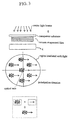
- Fig. 12 shows, in schematic form, a known arrangement of an irradiation device which emits polarized light and executes optical alignment of the alignment layer of a liquid crystal cell element.
- an irradiation device 10 has a lamp 1 which emits light which contains UV radiation emitted which is focussed by an oval focusing mirror 2, reflected by a first planar mirror 3, and is incident on an integrator lens 4 (which may also be called a fly eye lens).
- the light emerging from the integrator lens 4 is incident via a shutter 5 and via a second planar mirror 6 on a collimation lens 7, which converts the light into parallel light, which is incident on a polarization element 8.
- the polarized light emerging from the polarization element 8 is incident on a workpiece W, such as a liquid crystal cell element or the like.
- a primary object of the invention is to devise an irradiation device for an alignment layer of a liquid crystal cell element in which the need for a large polarization element can be avoided.
- the polarization element can be located in an area in which the light is focussed (i.e. in the vicinity of the integrator lens). However, one such location at which the light is focussed is hot. Therefore, either a multilayer film (an interference film) or a polarization element in which several glass plates are placed at the Brewster angle relative to one another, or the like, are used.
- a multilayer film an interference film
- a polarization element in which several glass plates are placed at the Brewster angle relative to one another, or the like, are used.
- parallel light is defined as light in which beams in the optical path which emerge from the center of the light source and which are each incident on any point on the surface to be irradiated are parallel to one another on the light incidence side of the surface to be irradiated.
- These beams in the optical path which emerge from the center of the light source are hereinafter called “center light beams.”
- the proportion of nonpolarized light is large in the outside peripheral area of the region to be irradiated.
- the illuminance of a given portion of the polarized light decreases and the polarization direction also changes.
- the polarization element using the multilayer film or the polarization element using the Brewster angle can be used as the polarization element. Furthermore, when the polarization element using the Brewster angle is used on the surface of at least one glass plate, a multilayer film can be formed with a high transmission factor for P-polarized light and a high reflectance factor for the S-polarized light and improvement of the extinction ratio can be attempted.
- the unpolarized light in the outside peripheral area of the polarization element is scattered over the entire region to be irradiated, by which the extinction ratio of the polarized light is made uniform over the entire region to be irradiated.
- the level of unpolarized light in the outside peripheral region is therefore below the level which has an adverse effect on optical alignment of the alignment layer.
- a polymer reaction can be suppressed outside of a specific direction to less than or equal to a stipulated amount. Therefore, local formation of faults in the outside peripheral area of the region to be irradiated can be prevented. In this way, yield can be increased.
- parallel beams can be allowed to be incident on the polarization element when the light is incident on the polarization element via the lens from which the parallel beams are emerging.
- uniform polarized light can be obtained. Therefore, local formation of faults in the outside peripheral area of the region to be irradiated can be prevented. In this way, yield can be increased.
- a dielectric multilayer film with a high transmission factor for P-polarized light and a high reflectance factor for S-polarized light can be vacuum evaporated on at least one glass plate.
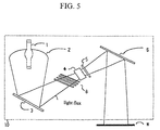
- Fig. 1 is a schematic of a first embodiment of the above described approach (1) in accordance with the present invention.
- a polarization element 8 using a multilayer film is located on the incidence side of an integrator lens 4.
- a bandpass filter 11 is located on the outlet side of a shutter 5. This bandpass filter 11 screens light which is polarized by the polarization element 8 and which lies in a wavelength range outside a certain (stipulated) wavelength range.
- the bandpass filter 11 can be placed in any position in the optical path between the oval focusing mirror 2 and a workpiece W. In the figure, the light which contains the UV radiation emitted from a lamp 1 is focused by the oval focusing mirror 2, reflected by a first planar mirror 3 and is incident on the polarization element 8 using the multilayer film.
- the light interference of the multilayer film is used.
- a portion of the polarized light with a certain wavelength range is screened or attenuated.
- the certain wavelength range in which this portion of polarized light is screened or attenuated is conventionally a few dozen nm to a few hundred and some ten nm, and therefore has a low width.
- a lamp with an emission range in a wide wavelength range such as a super-high pressure mercury lamp, a xenon lamp or the like, is combined with a polarization element and used, the light in the wavelength range outside the certain wavelength range passes through the polarization element without being polarized.
- the bandpass filter 11 it is therefore necessary to additionally use the bandpass filter 11 to screen the light of wavelengths that are outside of the certain wavelength range. Furthermore, instead of the bandpass filter 11, a wavelength selection mirror can be used.
- the wavelength characteristic of this bandpass filter lies in adequately screening the unpolarized light emerging from the polarization element.
- the light incident on the polarization element 8 is not parallel light because it was focused by the oval focusing mirror 2 and was reflected by the first planar mirror 3. Therefore, in the vicinity of the optical axis of the area to be irradiated in a certain wavelength range, polarized light is obtained, while unpolarized light is obtained outside of the peripheral area.
- the angle of incidence of the light incident on the multilayer film of the polarization element 8 changes, the length of the path of the incident light in the film (optical thickness of the film) changes. Accordingly, the wavelength range in which interference takes place (the wavelength which can screen or attenuate a certain portion of the polarized light) changes. This circumstance is called the "shift of the screening wavelength characteristic of the multilayer film.”
- the light passes unchanged through the polarization element without being polarized, even if the light is in a certain wavelength range.
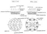
- Fig. 2 (a) is a schematic of the polarization direction in the area to be irradiated in the case in which parallel light has been incident on the polarization element using a multilayer film (an interference film).
- Fig. 2 (b) is a schematic of the polarization direction in the region to be irradiated in the case in which scattered light has been incident on the polarization element using a multilayer film (an interference film). The polarization direction is shown using arrows in the drawings.
- the polarization direction in the region to be irradiated is the same over the entire region, as shown in Fig. 2 (a).
- polarized light is obtained as shown in Fig. 2 (b).
- the angle of incidence is however greater, the closer the approach to the outer peripheral area of the region to be irradiated.
- unpolarized light is obtained in the outer peripheral area.
- polarized light is obtained, while in the outer peripheral area, unpolarized light is obtained.
- the light emerging from the polarization element 8 is incident on the integrator lens 4 which makes distribution of the portion of unpolarized light or distribution of illuminance of the polarized light in a certain direction and the distribution of the polarization direction uniform. Therefore, the unpolarized light in the outer peripheral area of polarization element 8 is scattered by the action of the integrator lens 4 over the entire region to be irradiated, by which the extinction ratio of the polarized light over the entire region to be irradiated is made uniform.
- the directivity of the portion of unpolarized light and the directivity of the portion of polarized light are added to one another by the integrator lens 4 as is illustrated in Figs. 2 (a) and 2(b).
- the polarization direction is made uniform over the entire region to be irradiated.
- the light emerging from the integrator lens 4 is incident via the shutter 5 on the bandpass filter 11.
- the light in a certain wavelength range which has passed through the bandpass filter 11 is incident via a second planar mirror 6 on a workpiece W, such as a liquid crystal cell element or the like.
- the light incident on the workpiece W is light which contains a portion of unpolarized light and a portion of polarized light.
- the extinction ratio of the polarized light over the entire region to be irradiated is uniform. If the extinction ratio of the polarized light with which the alignment layer is irradiated has a certain value, optical alignment of the alignment layer can be performed. Thus, optical alignment of the entire region of the workpiece W can be produced without disruption.
- one pixel is divided into two or more pixels and the alignment direction of the liquid crystals is changed in the respective pixel formed by division, by which the angle of view field of the liquid crystal display is improved.
- This process is called the pixel division process or multi-domain method.
- the polarization element 8 need not be located on the outlet side of the collimating lens 7.
- the polarization element 8 can be located on the incidence side of the integrator lens 4 with a small light flux.
- the polarization element 8 is located on the incidence side of the integrator lens 4 with a small light flux.
- the distribution of the portion of unpolarized light or distribution of illuminance of the polarized light in a certain direction and the distribution of the polarization direction are made uniform by the integrator lens 4. Therefore, using a small polarization element, optical alignment of the entire region of workpiece W can be produced without disruption.
- use of a polarization element using light interference of an inorganic, multilayer film as the polarization element 8 prevents the polarization element from degrading when irradiated with strong light or UV radiation and at a high temperature of the polarization element.
- Fig. 5 schematically shows a second embodiment of the above described approach (1) in accordance with the invention.
- a polarization element with the Brewster angle is used.
- Fig. 5 the same parts as in Fig. 1 are provided with the same reference numbers.
- the polarization element 8 using the Brewster angle is located on the incidence side of the integrator lens 4.
- the light which contains the UV radiation emitted from the lamp 1 is focused by the oval focusing mirror 2 and is reflected by the first planar mirror 3 and the scattered light is incident on the polarization element 8 using the Brewster angle.
- the polarization element 8 transmits essentially 100% of the polarized light, when the angle of incidence of the incident light is the Brewster angle. However, if it is outside the Brewster angle, the degree of transmission of the portion of polarized light decreases. Furthermore, the polarization direction changes as a function of the angle of incidence of the incident light.
- the polarization direction in the outer peripheral region of the polarization element changes as a function of the conditions of the arrangement of the polarization element and of the angle of incidence of the light. If, for example, scattered light is incident on a polarization element which made of 15 fused silica glass plates, the polarization direction on both sides of the region to be irradiated is tilted by a maximum of 6°, as is shown in Fig. 6.
- the polarization direction is therefore determined by the direction of the resultant of the vector of the S-polarized light and the vector of the P-polarized light. The polarization direction is therefore changed.
- Fig. 7 (a) is a schematic of the polarization direction in the region to be irradiated in the case of incidence of parallel light on a polarization element using the Brewster angle.
- Fig. 7 (b) is a schematic of the polarization direction in the region to be irradiated in the case of incidence of scattered light on a polarization element using the Brewster angle. The polarization direction is shown by arrows in the drawings.
- the polarization direction in the region to be irradiated is the same over the entire region. If, on the other hand, scattered light is incident on the polarization element, the ratio of the portion of S-polarized light to the portion of P-polarized light changes more, the closer the approach to the outer area of the region to be irradiated, as is shown in Fig. 7(b).
- the direction of the arrows in the representation is designated P-polarized light
- the portion of S-polarized light gradually increases.
- the glass plates are tilted with respect to the optical axis by the Brewster angle. With only one glass plate, a low polarization separation efficiency is obtained. To increase the extinction ratio, therefore, usually several glass plates are arranged in parallel at a distance from one another, as is illustrated in Figs. 7 (a) and 7(b).
- the amount of irradiation in the outer peripheral area of the region to be irradiated decreases more than in the middle area of the region to be irradiated.
- the polarization direction in the middle area of the region to be irradiated therefore differs from the polarization direction in the outer peripheral area of the region to be irradiated, as is illustrated in Fig. 7(b).
- the light emerging from the polarization element 8 is incident on the integrator lens 4. Since the integrator lens 4 makes the distribution of the portion of unpolarized light or distribution of illuminance of the polarized light in a certain direction and the distribution of the polarization direction uniform, the low illuminance of the polarized light in the outer peripheral area of the polarization element 8 and the high illuminance of the polarized light in the center region are made uniform.
- the polarized light with different polarization directions is scattered over the entire region to be irradiated, by which the extinction ratio of the polarized light in a certain direction is made uniform over the entire region to be irradiated.
- the direction of the polarization is made uniform over the entire region to be irradiated.
- the light emerging from the integrator lens 4 is incident via the shutter 5 and the second planar mirror 6 onto a workpiece W, such as a liquid crystal cell element or the like.
- the light incident on the workpiece W is formed by adding the portions of polarized light with different directions, as is illustrated in Fig. 8. If the extinction ratio of the polarized light with which the alignment layer is irradiated has a certain value, optical alignment of the alignment layer can be achieved.
- optical alignment of the entire region of the workpiece W can be performed without disruption.
- the collimating lens 7 which is used to obtain parallel light is located on the outlet side of the second planar mirror 6, as was described relative to Fig. 4.
- the parallel light emerging from the collimating lens 7 is emitted via the mask M onto the workpiece W.
- Optical alignment is produced in the respective pixel formed by division.
- the polarization element 8 is located on the incidence side of the integrator lens 4 with a small light flux, which makes distribution of the portion of unpolarized light or distribution of illuminance of the polarized light in a certain direction and the distribution of the polarization direction uniform. Therefore, using a small polarization element, optical alignment of the entire region of the workpiece W can be obtained without disruption. Furthermore, using a polarization element in which the glass plates are used as the inorganic material prevents degradation of the polarization element upon irradiation with strong light or UV radiation and at a high temperature.
- a film with a high transmission factor for P-polarized light and a high reflectance factor for S-polarized light can be vacuum evaporated.
- Figs. 9 (a) and (b) each show schematically an embodiment in which in a polarization element using the Brewster angle which consists of several glass plates, a multilayer film with a high transmission factor for P-polarized light and a high reflection factor for S-polarized light is vacuum evaporated on a glass plate to improve the extinction ratio.
- a vacuum evaporated film with a physical layer thickness of roughly 1 micron can be used here; it is produced by layering hafnium oxide (HfO 2 ) and silicon dioxide (SiO 2 ) twelve times on top of one another.
- the multilayer film need not necessarily be formed on the surface of the first glass plate. It can also be formed on the surface or the back of any glass plate starting with the second glass plate. Furthermore, it can be formed on the surfaces of several glass plates. If, for example, on the last glass plate on the light emergence side, a multilayer film is formed, ignoring reflection from the surface of the first glass plate on the incidence side, the portion of reflected S-polarized light is reflected over several paths by the surfaces and the backs of other glass plates and reaches the glass plate on the last stage, as is shown in Fig. 9(b). Since it is reflected by the multilayer film which is located on the back of the glass plate on the last stage, the portion of S-polarized light emerging from the polarization element 8 can be greatly reduced, as is shown in Fig. 9(a).
- the portion of S-polarized light is not reduced as effectively as in vacuum evaporation of a multilayer film on the surface of the first glass plate.
- the reason for this is that the portion of S-polarized light reflected by the multilayer film undergoes multi-path reflection by the top glass plates on the incidence side and in part returns to the glass plate on the lowermost stage. Therefore, it is effective to vacuum evaporate the multilayer film on the glass plate that is as uppermost as possible (on the incidence side) to reduce the portion of S-polarized light.
- the glass plate on which the multilayer film is vacuum evaporated should be located under several glass plates, i.e. where is the optimal location:
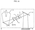
- Fig. 10 schematically shows one embodiment thereof.
- the same parts as in Figs. 1 and 12 are provided with the same reference numbers.
- the integrator lens 4 on the incidence side of the integrator lens 4, there are an input lens 21 for converting the convergence light focussed by the oval focusing mirror 2 into parallel light and a polarization element 8 using a multilayer film or the Brewster angle.
- the light which contains the UV radiation emitted from the lamp 1 is focused by the oval focusing mirror 2, is reflected by the first planar mirror 3 and is incident on the input lens 21.
- the input lens 21 converts the light focused by the oval focusing mirror 2 into parallel light and allows it to be incident on the polarization element 8.
- the polarization element 8 is comprised of a multilayer film or is produced using the Brewster angle. In the case of a polarization element using the multilayer film, by means of an interference effect, a portion of polarized light with certain wavelengths is screened or attenuated.
- the light emerging from the polarization element 8 is incident on the integrator lens 4, by which scattered light emerges. This emerged light is incident via a shutter 5 on a second planar mirror 6.
- the light reflected by the second planar mirror 6 is emitted onto the workpiece W, such as a liquid crystal cell element or the like.
- the polarization direction of the polarized light emerging from the polarization element 8 is uniform over the entire region to be irradiated. Therefore, trouble-free optical alignment of the entire region of the workpiece W can be performed.
- a polarization element utilizing light interference of an inorganic multilayer film, or using the Brewster angle as the polarization element 8 prevents degradation of the polarization element for irradiation with strong light or UV radiation and at a high temperature.
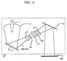
- Fig. 11 schematically shows one embodiment thereof.
- the same parts as in Figs. 1, 10 and 12 are provided with the same reference numbers.
- a first lens 22 for converting the light emerging from the integrator lens 4 into parallel light and a polarization element 8 are located on the outlet side of integrator lens 4.
- the light emitted form the lamp 1, which contains the UV radiation 1, is focused by an oval focusing mirror 2, reflected by a first planar mirror 3, and is incident on an integrator lens 4.
- the light emerging from the integrator lens 4 is incident on a first lens 22, is converted into parallel light, and is incident on the polarization element 8.
- the polarization element 8 is produced, as described above, using a multilayer film or using the Brewster angle.
- the parallel light emerging from the polarization element 8 is incident on the second lens 23 and is converted into scattered light; its exit light is incident via shutter 5 on the second planar mirror 6.
- the light reflected by the second planar mirror 6 is emitted onto a workpiece W, such as a liquid crystal cell element or the like.
- a workpiece W such as a liquid crystal cell element or the like.
- the polarization direction of the polarized light emerging from the polarization element 8 is uniform over the entire region to be irradiated. Therefore, trouble-free optical alignment of the entire region of the workpiece W can be achieved.
- the flux of light emerging from the polarization element 8 can propagate and the required irradiation area on the light irradiation surface ensured.
- a collimating lens 7 for obtaining parallel light.
- the parallel light emerging from the collimating lens 7 is emitted onto the workpiece W via a mask M.
- optical alignment is obtained.
Landscapes
- Physics & Mathematics (AREA)
- General Physics & Mathematics (AREA)
- Optics & Photonics (AREA)
- Nonlinear Science (AREA)
- Chemical & Material Sciences (AREA)
- Crystallography & Structural Chemistry (AREA)
- Engineering & Computer Science (AREA)
- Manufacturing & Machinery (AREA)
- Spectroscopy & Molecular Physics (AREA)
- Mathematical Physics (AREA)
- Liquid Crystal (AREA)
- Polarising Elements (AREA)
Priority Applications (1)
| Application Number | Priority Date | Filing Date | Title |
|---|---|---|---|
| EP06022140A EP1750163A3 (de) | 1997-10-29 | 1998-10-28 | Bestrahlungsvorrichtung für eine Ausrichtungsschicht eines Flüssigkristallzellenelements |
Applications Claiming Priority (12)
| Application Number | Priority Date | Filing Date | Title |
|---|---|---|---|
| JP29662097 | 1997-10-29 | ||
| JP29662197 | 1997-10-29 | ||
| JP29662097 | 1997-10-29 | ||
| JP29662197 | 1997-10-29 | ||
| JP296621/97 | 1997-10-29 | ||
| JP296620/97 | 1997-10-29 | ||
| JP9887598A JP2960392B2 (ja) | 1997-10-29 | 1998-04-10 | 液晶表示素子の配向膜光配向用偏光光照射装置 |
| JP9887598 | 1998-04-10 | ||
| JP98875/98 | 1998-04-10 | ||
| JP9887498 | 1998-04-10 | ||
| JP98874/98 | 1998-04-10 | ||
| JP9887498A JP2928226B2 (ja) | 1997-10-29 | 1998-04-10 | 液晶表示素子の配向膜光配向用偏光光照射装置 |
Related Child Applications (1)
| Application Number | Title | Priority Date | Filing Date |
|---|---|---|---|
| EP06022140A Division EP1750163A3 (de) | 1997-10-29 | 1998-10-28 | Bestrahlungsvorrichtung für eine Ausrichtungsschicht eines Flüssigkristallzellenelements |
Publications (3)
| Publication Number | Publication Date |
|---|---|
| EP0913720A2 true EP0913720A2 (de) | 1999-05-06 |
| EP0913720A3 EP0913720A3 (de) | 1999-12-08 |
| EP0913720B1 EP0913720B1 (de) | 2007-06-20 |
Family
ID=27468678
Family Applications (2)
| Application Number | Title | Priority Date | Filing Date |
|---|---|---|---|
| EP06022140A Withdrawn EP1750163A3 (de) | 1997-10-29 | 1998-10-28 | Bestrahlungsvorrichtung für eine Ausrichtungsschicht eines Flüssigkristallzellenelements |
| EP98120401A Expired - Lifetime EP0913720B1 (de) | 1997-10-29 | 1998-10-28 | Bestrahlungsvorrichtung für eine Orientierungsschicht für Flüssigkristallanzeigen |
Family Applications Before (1)
| Application Number | Title | Priority Date | Filing Date |
|---|---|---|---|
| EP06022140A Withdrawn EP1750163A3 (de) | 1997-10-29 | 1998-10-28 | Bestrahlungsvorrichtung für eine Ausrichtungsschicht eines Flüssigkristallzellenelements |
Country Status (5)
| Country | Link |
|---|---|
| US (1) | US6190016B1 (de) |
| EP (2) | EP1750163A3 (de) |
| KR (1) | KR100510888B1 (de) |
| DE (1) | DE69837961T2 (de) |
| TW (1) | TW536644B (de) |
Cited By (5)
| Publication number | Priority date | Publication date | Assignee | Title |
|---|---|---|---|---|
| EP1172684A1 (de) * | 2000-07-12 | 2002-01-16 | Ushiodenki Kabushiki Kaisha | Bestrahlungsvorrichtung zur Erzeugung von polarisiertem Licht für eine Orientierungsschicht für Flüssigkristallanzeigen |
| EP1217424A1 (de) * | 2000-12-22 | 2002-06-26 | Ushiodenki Kabushiki Kaisha | Belichtungsapparatur für polarisiertes Licht für eine optische Ausrichtung |
| WO2003021331A1 (en) * | 2001-08-29 | 2003-03-13 | Polaroid Corporation | Polarized exposure for web manufacture |
| EP1215524A3 (de) * | 2000-12-12 | 2004-03-17 | Ushiodenki Kabushiki Kaisha | Bestrahlungsvorrichtung für polarisiertes Licht mit einem Polarisationsstrahlenteiler |
| EP1162491A3 (de) * | 2000-06-06 | 2004-04-14 | Ushiodenki Kabushiki Kaisha | Bestrahlungsapparatur mit polarisiertem Licht |
Families Citing this family (17)
| Publication number | Priority date | Publication date | Assignee | Title |
|---|---|---|---|---|
| US7061679B1 (en) * | 1998-05-27 | 2006-06-13 | Lg. Philips Lcd Co., Ltd. | Light irradiating device |
| US6874899B2 (en) * | 2002-07-12 | 2005-04-05 | Eastman Kodak Company | Apparatus and method for irradiating a substrate |
| US6797971B2 (en) * | 2002-07-18 | 2004-09-28 | Fusion Uv Systems, Inc. | Apparatus and method providing substantially two-dimensionally uniform irradiation |
| US6649921B1 (en) | 2002-08-19 | 2003-11-18 | Fusion Uv Systems, Inc. | Apparatus and method providing substantially two-dimensionally uniform irradiation |
| US6943930B2 (en) * | 2002-09-12 | 2005-09-13 | Eastman Kodak Company | Method and system for fabricating optical film using an exposure source and reflecting surface |
| US6844913B2 (en) * | 2003-04-24 | 2005-01-18 | Eastman Kodak Company | Optical exposure apparatus for forming an alignment layer |
| US6717161B1 (en) | 2003-04-30 | 2004-04-06 | Fusion Uv Systems, Inc. | Apparatus and method providing substantially uniform irradiation of surfaces of elongated objects with a high level of irradiance |
| JP2005128271A (ja) * | 2003-10-24 | 2005-05-19 | Ushio Inc | 光配向用偏光光照射装置および光配向用偏光光照射装置における偏光軸の調整方法 |
| US7413317B2 (en) * | 2004-06-02 | 2008-08-19 | 3M Innovative Properties Company | Polarized UV exposure system |
| JP4622409B2 (ja) | 2004-09-16 | 2011-02-02 | ウシオ電機株式会社 | 光配向方法 |
| JP2006202628A (ja) * | 2005-01-21 | 2006-08-03 | Dainippon Printing Co Ltd | 偏光光照射装置、偏光光照射方法、光配向膜、及び位相差フィルム |
| JP5181138B2 (ja) * | 2006-11-02 | 2013-04-10 | 友達光電股▲ふん▼有限公司 | 液晶パネル製造装置及び液晶パネルの製造方法 |
| KR101383930B1 (ko) * | 2008-12-24 | 2014-04-10 | 엘지디스플레이 주식회사 | 광 조사 장치 |
| JP6578820B2 (ja) * | 2015-08-28 | 2019-09-25 | ウシオ電機株式会社 | 紫外線照射器および紫外線照射装置 |
| CN106248616B (zh) * | 2016-09-27 | 2017-10-24 | 深圳市太赫兹科技创新研究院有限公司 | 太赫兹全偏振态检测光谱仪 |
| CN112992083B (zh) * | 2021-04-01 | 2022-11-04 | 上海天马微电子有限公司 | 驱动电路、显示面板以及显示装置 |
| CN116520612B (zh) * | 2023-04-20 | 2024-05-28 | 成都瑞波科材料科技有限公司 | 光学组件及光学膜处理装置 |
Family Cites Families (17)
| Publication number | Priority date | Publication date | Assignee | Title |
|---|---|---|---|---|
| US2982178A (en) * | 1952-11-14 | 1961-05-02 | Marks Polarized Corp | Multi-layer light polarizing structure |
| US4195422A (en) * | 1976-12-20 | 1980-04-01 | Laspo Ag | System for simulating weapon firing |
| US4851882A (en) * | 1985-12-06 | 1989-07-25 | Canon Kabushiki Kaisha | Illumination optical system |
| JPH0355921Y2 (de) * | 1986-11-11 | 1991-12-13 | ||
| JP2696360B2 (ja) * | 1988-10-28 | 1998-01-14 | 旭光学工業株式会社 | 照明光学装置 |
| US5311217A (en) * | 1991-12-23 | 1994-05-10 | Xerox Corporation | Variable attenuator for dual beams |
| US5339441A (en) * | 1992-07-02 | 1994-08-16 | Advanced Intervention Systems, Inc. | Polarizing device with optically contacted thin film interface for high power density ultraviolet light |
| AU1866395A (en) * | 1993-12-21 | 1995-07-10 | Minnesota Mining And Manufacturing Company | Multilayered optical film |
| US5909314A (en) | 1994-02-15 | 1999-06-01 | Dai Nippon Printing Co., Ltd. | Optical functional materials and process for producing the same |
| JPH07318861A (ja) | 1994-05-19 | 1995-12-08 | Canon Inc | 板状偏光素子、該板状偏光素子を用いた偏光照明装置および前記板状偏光素子を用いたプロジェクター |
| KR0132824B1 (ko) * | 1994-09-08 | 1998-04-16 | 김광호 | 액정프로젝터 |
| JP3608580B2 (ja) * | 1995-03-22 | 2005-01-12 | 株式会社ニコン | 照明光学装置、露光装置、露光方法、及びフライアイレンズ |
| KR100379873B1 (ko) | 1995-07-11 | 2003-08-21 | 우시오덴키 가부시키가이샤 | 막질개량방법 |
| FR2744536B1 (fr) | 1996-02-01 | 2004-03-05 | Lg Electronics Inc | Dispositif d'irradiation ultraviolette destine a un procede de photo-alignement, et methode d'irradiation utilisant ce dispositif |
| US5731405A (en) | 1996-03-29 | 1998-03-24 | Alliant Techsystems Inc. | Process and materials for inducing pre-tilt in liquid crystals and liquid crystal displays |
| KR0176609B1 (ko) * | 1996-07-16 | 1999-05-15 | 삼성전자주식회사 | 액정프로젝터 |
| JP3146998B2 (ja) * | 1996-09-12 | 2001-03-19 | ウシオ電機株式会社 | 液晶表示素子の配向膜光配向用偏光光照射装置 |
-
1998
- 1998-09-15 TW TW087115362A patent/TW536644B/zh not_active IP Right Cessation
- 1998-10-27 US US09/179,201 patent/US6190016B1/en not_active Expired - Lifetime
- 1998-10-28 KR KR10-1998-0045534A patent/KR100510888B1/ko not_active Expired - Fee Related
- 1998-10-28 EP EP06022140A patent/EP1750163A3/de not_active Withdrawn
- 1998-10-28 EP EP98120401A patent/EP0913720B1/de not_active Expired - Lifetime
- 1998-10-28 DE DE69837961T patent/DE69837961T2/de not_active Expired - Lifetime
Cited By (8)
| Publication number | Priority date | Publication date | Assignee | Title |
|---|---|---|---|---|
| EP1162491A3 (de) * | 2000-06-06 | 2004-04-14 | Ushiodenki Kabushiki Kaisha | Bestrahlungsapparatur mit polarisiertem Licht |
| EP1172684A1 (de) * | 2000-07-12 | 2002-01-16 | Ushiodenki Kabushiki Kaisha | Bestrahlungsvorrichtung zur Erzeugung von polarisiertem Licht für eine Orientierungsschicht für Flüssigkristallanzeigen |
| US6567216B2 (en) | 2000-07-12 | 2003-05-20 | Ushiodenki Kabushiki Kaisha | Polarization element of an irradiation device for polarized light for optical alignment of a liquid crystal alignment layer |
| EP1215524A3 (de) * | 2000-12-12 | 2004-03-17 | Ushiodenki Kabushiki Kaisha | Bestrahlungsvorrichtung für polarisiertes Licht mit einem Polarisationsstrahlenteiler |
| US6724530B2 (en) | 2000-12-12 | 2004-04-20 | Ushiodenki Kabushiki Kaisha | Polarized light illuminator with a polarized light beam splitter |
| EP1217424A1 (de) * | 2000-12-22 | 2002-06-26 | Ushiodenki Kabushiki Kaisha | Belichtungsapparatur für polarisiertes Licht für eine optische Ausrichtung |
| WO2003021331A1 (en) * | 2001-08-29 | 2003-03-13 | Polaroid Corporation | Polarized exposure for web manufacture |
| US6791749B2 (en) | 2001-08-29 | 2004-09-14 | Delpico Joseph | Polarized exposure for web manufacture |
Also Published As
| Publication number | Publication date |
|---|---|
| DE69837961D1 (de) | 2007-08-02 |
| US6190016B1 (en) | 2001-02-20 |
| EP0913720A3 (de) | 1999-12-08 |
| EP1750163A2 (de) | 2007-02-07 |
| DE69837961T2 (de) | 2008-02-28 |
| EP0913720B1 (de) | 2007-06-20 |
| KR19990037466A (ko) | 1999-05-25 |
| TW536644B (en) | 2003-06-11 |
| EP1750163A3 (de) | 2007-02-21 |
| KR100510888B1 (ko) | 2005-10-26 |
Similar Documents
| Publication | Publication Date | Title |
|---|---|---|
| US6190016B1 (en) | Irradiation device for an alignment layer of a liquid crystal cell element | |
| KR100454692B1 (ko) | 액정표시소자의배향막광배향용편광광조사장치 | |
| KR100189278B1 (ko) | 투영형 칼라 표시 장치 | |
| JP4122041B2 (ja) | 表示装置 | |
| US20010049061A1 (en) | Method for producing hologram lens, method for producing hologram color filter, and space light modulating apparatuses using the hologram lens and the hologram color filter respectively | |
| JP2928226B2 (ja) | 液晶表示素子の配向膜光配向用偏光光照射装置 | |
| JP2003337223A (ja) | パターン化されたパッシブ位相板の製造方法およびその方法により製造された位相板 | |
| JP2960392B2 (ja) | 液晶表示素子の配向膜光配向用偏光光照射装置 | |
| EP1289312B1 (de) | Optischer Farbenteiler, optisches System zur Bildanzeige und Projektionsbildanzeigegerät | |
| US7894029B2 (en) | Apparatus for optically arranging surface of alignment film and method for manufacturing liquid crystal display device using the same | |
| US6567216B2 (en) | Polarization element of an irradiation device for polarized light for optical alignment of a liquid crystal alignment layer | |
| JP2927679B2 (ja) | 液晶表示装置 | |
| US6724530B2 (en) | Polarized light illuminator with a polarized light beam splitter | |
| JP2002014345A (ja) | 投射型液晶表示装置 | |
| JP2005157378A (ja) | 偏光変換光学系 | |
| WO2000050953A1 (fr) | Affichage a cristaux liquides a emission | |
| KR960005937B1 (ko) | 투영형 컬러 화상표시장치 | |
| JP4135557B2 (ja) | 光配向用偏光光照射装置 | |
| US20090079912A1 (en) | Liquid crystal display device | |
| US20020080486A1 (en) | Polarized light illuminator for optical alignment | |
| KR20050107733A (ko) | 반사형 액정 표시 소자 및 액정 표시 장치 | |
| JPH10221673A (ja) | 投射型カラー画像表示装置 | |
| JP2000162549A (ja) | 偏光変換素子、それを用いた表示装置および投射型表示装置 | |
| JP2007101834A (ja) | マイクロレンズの製造方法、マスク、マイクロレンズ、空間光変調装置及びプロジェクタ | |
| KR101213104B1 (ko) | 마이크로렌즈 어레이 시트 및 이를 이용한 액정 표시 장치 |
Legal Events
| Date | Code | Title | Description |
|---|---|---|---|
| PUAI | Public reference made under article 153(3) epc to a published international application that has entered the european phase |
Free format text: ORIGINAL CODE: 0009012 |
|
| AK | Designated contracting states |
Kind code of ref document: A2 Designated state(s): DE FR GB IT NL |
|
| AX | Request for extension of the european patent |
Free format text: AL;LT;LV;MK;RO;SI |
|
| PUAL | Search report despatched |
Free format text: ORIGINAL CODE: 0009013 |
|
| AK | Designated contracting states |
Kind code of ref document: A3 Designated state(s): AT BE CH CY DE DK ES FI FR GB GR IE IT LI LU MC NL PT SE |
|
| AX | Request for extension of the european patent |
Free format text: AL;LT;LV;MK;RO;SI |
|
| RIC1 | Information provided on ipc code assigned before grant |
Free format text: 6G 02F 1/1335 A, 6G 02B 5/30 B, 6G 02B 27/28 B, 6G 02F 1/1337 B |
|
| 17P | Request for examination filed |
Effective date: 20000512 |
|
| AKX | Designation fees paid |
Free format text: DE FR GB IT NL |
|
| 17Q | First examination report despatched |
Effective date: 20011106 |
|
| GRAP | Despatch of communication of intention to grant a patent |
Free format text: ORIGINAL CODE: EPIDOSNIGR1 |
|
| RIN1 | Information on inventor provided before grant (corrected) |
Inventor name: MIZUNO, OSAMU Inventor name: SUZUKI, SHINJI |
|
| GRAS | Grant fee paid |
Free format text: ORIGINAL CODE: EPIDOSNIGR3 |
|
| GRAA | (expected) grant |
Free format text: ORIGINAL CODE: 0009210 |
|
| AK | Designated contracting states |
Kind code of ref document: B1 Designated state(s): DE FR GB IT NL |
|
| REG | Reference to a national code |
Ref country code: GB Ref legal event code: FG4D |
|
| REF | Corresponds to: |
Ref document number: 69837961 Country of ref document: DE Date of ref document: 20070802 Kind code of ref document: P |
|
| ET | Fr: translation filed | ||
| PLBE | No opposition filed within time limit |
Free format text: ORIGINAL CODE: 0009261 |
|
| STAA | Information on the status of an ep patent application or granted ep patent |
Free format text: STATUS: NO OPPOSITION FILED WITHIN TIME LIMIT |
|
| PG25 | Lapsed in a contracting state [announced via postgrant information from national office to epo] |
Ref country code: IT Free format text: LAPSE BECAUSE OF FAILURE TO SUBMIT A TRANSLATION OF THE DESCRIPTION OR TO PAY THE FEE WITHIN THE PRESCRIBED TIME-LIMIT Effective date: 20070620 |
|
| 26N | No opposition filed |
Effective date: 20080325 |
|
| PGFP | Annual fee paid to national office [announced via postgrant information from national office to epo] |
Ref country code: DE Payment date: 20101020 Year of fee payment: 13 |
|
| PGFP | Annual fee paid to national office [announced via postgrant information from national office to epo] |
Ref country code: GB Payment date: 20101027 Year of fee payment: 13 |
|
| PGFP | Annual fee paid to national office [announced via postgrant information from national office to epo] |
Ref country code: FR Payment date: 20111103 Year of fee payment: 14 Ref country code: NL Payment date: 20111020 Year of fee payment: 14 |
|
| REG | Reference to a national code |
Ref country code: NL Ref legal event code: V1 Effective date: 20130501 |
|
| GBPC | Gb: european patent ceased through non-payment of renewal fee |
Effective date: 20121028 |
|
| REG | Reference to a national code |
Ref country code: FR Ref legal event code: ST Effective date: 20130628 |
|
| PG25 | Lapsed in a contracting state [announced via postgrant information from national office to epo] |
Ref country code: GB Free format text: LAPSE BECAUSE OF NON-PAYMENT OF DUE FEES Effective date: 20121028 Ref country code: DE Free format text: LAPSE BECAUSE OF NON-PAYMENT OF DUE FEES Effective date: 20130501 |
|
| REG | Reference to a national code |
Ref country code: DE Ref legal event code: R119 Ref document number: 69837961 Country of ref document: DE Effective date: 20130501 |
|
| PG25 | Lapsed in a contracting state [announced via postgrant information from national office to epo] |
Ref country code: NL Free format text: LAPSE BECAUSE OF NON-PAYMENT OF DUE FEES Effective date: 20130501 Ref country code: FR Free format text: LAPSE BECAUSE OF NON-PAYMENT OF DUE FEES Effective date: 20121031 |