EP0913972A2 - Mehrträger-Funkübertragungssystem - Google Patents
Mehrträger-Funkübertragungssystem Download PDFInfo
- Publication number
- EP0913972A2 EP0913972A2 EP98120486A EP98120486A EP0913972A2 EP 0913972 A2 EP0913972 A2 EP 0913972A2 EP 98120486 A EP98120486 A EP 98120486A EP 98120486 A EP98120486 A EP 98120486A EP 0913972 A2 EP0913972 A2 EP 0913972A2
- Authority
- EP
- European Patent Office
- Prior art keywords
- data
- axis direction
- subcarriers
- phase difference
- modulation process
- Prior art date
- Legal status (The legal status is an assumption and is not a legal conclusion. Google has not performed a legal analysis and makes no representation as to the accuracy of the status listed.)
- Withdrawn
Links
Images





Classifications
-
- H—ELECTRICITY
- H04—ELECTRIC COMMUNICATION TECHNIQUE
- H04L—TRANSMISSION OF DIGITAL INFORMATION, e.g. TELEGRAPHIC COMMUNICATION
- H04L27/00—Modulated-carrier systems
- H04L27/26—Systems using multi-frequency codes
- H04L27/2601—Multicarrier modulation systems
- H04L27/2602—Signal structure
Definitions
- This invention relates to data communication methods, transmitters, and cellular radio communication systems, and more particularly, is suitable for use in a radio communication system such as a portable telephone system.
- an area providing communication services is segmented into cells with a predetermined size.
- Base stations as stationary radio stations are deployed within the cells, respectively.
- a portable telephone as a mobile radio station can communicate with the base station within the cell where the portable telephone exists.
- a so-called cellular system is constructed.
- various systems have been proposed as the communication system between a portable telephone and a base station.
- TDMA time division multiple access
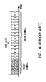
- a predetermined frequency channel is segmented temporally into frames (F0, F1, ...) each having a predetermined time interval.
- Each frame is further divided into time slots TS0 to TS3, each time slot has a predetermined time interval.
- the user uses the time slot to transmit a transmission signal.
- This system realizes a plurality of communications (so-called multiplex communication) by the same frequency channel and therefore utilizes frequency efficiently.
- time slot TS0 allocated for transmission is called transmission slot TX, while a block of data (i.e., data unit) that is sent with one transmission slot TX is called a slot.
- the transmitter and receiver of a radio communication system to transmit and receive data by taking an advantage of this TDMA system will be described with Figs. 2 and 3.
- the transmitter and receiver shown in Figs. 2 and 3 are mounted, for example, in the portable telephone and base station of a portable telephone system, respectively.
- the transmitter and the receiver are used in the Communication from a portable telephone to a base station (so-called uplink communication) and the communication from a base station to a portable telephone (so-called downlink communication).
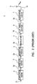
- the transmitter 1 is roughly constituted by a convolution coding circuit 2, an interleave buffer 3, a segmenting circuit 4, a modulation circuit 5, a pilot symbol adding circuit 6, a transmitting circuit 7, and an antenna 8.
- a data bit series S1 transmission data is first input to the convolution coding circuit 2.
- the convolution coding circuit 2 consists of a predetermined stage-number of shift registers and exclusive OR circuits.
- the convolution coding circuit 2 performs convolution coding on the input data bit series S1 and then outputs the resulting coded bit series S2 to the interleave buffer 3.
- the interleave buffer 3 stores the coded bit series S2 in its internal storage region in order. If the coded bit series S2 is stored in the entire storage region (i.e., if the coded bit series S2 is accumulated by a desired amount), then the order of the coded bit series S2 will be randomly rearranged (rearranging this order will hereinafter be referred to as interleaving). The resulting coded bit series S3 is output to the segmenting circuit 4.
- the interleave buffer 3 has a storage capacity equivalent to a plurality of slots so that the coded bit series S3 is dispersed to a plurality of transmission slots TX.
- the segmenting circuit 4 segments the coded bit series S3 at intervals of a predetermined number of bits in order to allocate the coded bit series S3 to transmission slots TX.
- the resulting coded bit group S4 is output to the modulation circuit 5 in order.
- the modulation circuit 5 performs a predetermined modulation process (e.g., a modulation process in a synchronous detection system such as QPSK modulation) on the supplied coded bit group S4 and then outputs the resulting data symbol group S5 to the pilot symbol adding circuit 6.
- a predetermined modulation process e.g., a modulation process in a synchronous detection system such as QPSK modulation
- the pilot symbol adding circuit 6 adds pilot symbols P as a header at the head of each symbol group (i.e., the head of data symbol I) of the data symbol group S5 segmented according to the transmission slots TX, and then outputs the resulting transmission group S6 to the transmitting circuit 7.
- the pilot symbols P added here are a known symbol pattern that has previously been known at the receiver side, and at the receiver side, these pilot symbols P are employed to estimate the characteristics of the transmission path (e.g., fading, etc.).
- the transmitting circuit 7 performs a filtering process on the transmission symbol group S6 added with these pilot symbols P in sequence and then performs a digital-to-analog conversion process on the transmission symbol group S6 to generate a transmission signal. And the transmitting circuit 7 performs a frequency transformation on the transmission signal, thereby generating a transmission signal S7 having a predetermined frequency channel. After this signal has been amplified to a predetermined electric power, it is transmitted through the antenna 8. In this manner, the transmission signal S7 is transmitted from the transmitter 1 in synchronization with the timing of the transmission slots TX.
- the receiver 10 is roughly constituted by an antenna 11, a receiving circuit 12, a transmission path estimating circuit 13, a demodulation circuit 14, a slot coupling circuit 15, a deinterleave buffer 16, and a Viterbi decoding circuit 17.
- the transmission signal S7 transmitted from the transmitter 1 is received by the antenna 11, and this is input to the receiving circuit 12 as a received signal S11.
- the receiving circuit 12 amplifies the input received signal S11 and then performs a frequency transformation on the received signal S11, thereby taking out a base band signal.
- the receiving circuit 12 performs a filtering process on the base band signal and then performs an analog-to-digital conversion process on the base band signal, thereby taking out a received symbol group S12 corresponding to the transmission symbol group S6.
- the received symbol group S12 is output to the transmission path estimating circuit 13.
- the transmission path estimating circuit 13 is one which investigates the characteristic of the transmission path and also performs an equivalent process according to the result of investigation.
- the transmission path estimating circuit 13 estimates the characteristic of the transmission path by making a reference to the pilot symbols P included in the received symbol group S12, and computes the inverted characteristic of the transmission path, based on the result of estimation.
- the transmission path estimating circuit 13 convolution-multiples a numerical value, which indicates the inverted characteristic of the transmission path, and each data symbol portion of the received symbol group S12, by using an equalizing circuit consisting of an equalizer. With this multiplication, the influence of fading caused on the transmission path is removed. With this process, the transmission path estimating circuit 13 restores the transmitted data symbol group S5 and outputs this to the modulation circuit 14 as a received data symbol group S13.
- the modulation circuit 14 performs a predetermined modulation process on the received data symbol group S13, thereby restoring the coded bit group S14 corresponding to the coded bit group S4 on the transmitter side.
- the coded bit group S14 is output to the slot coupling circuit 15.
- each bit in the coded bit group S14 is not a binary signal such as a logic 0 or a logic 1 but has become a multi-level signal because of a noise component added on the transmission path.
- the slot coupling circuit 15 is one which couples the group S14 of separate coded bits obtained in a slot unit so that they become a series signal. If the coded bit group S14 is accumulated by an amount corresponding to the storage capacity of the deinterleave buffer 16 of the latter stage, then the coded bit group S14 will be coupled together. The resulting code bit series S15 is output to the deinterleave buffer 16.
- the deinterleave buffer 16 has a storage capacity equivalent to a plurality of slots.
- the deinterleave buffer 16 stores the supplied coded bit series S15 in its internal storage region in series and then rearrange the order of the coded bit series S15 in the order opposite the rearrangement made by the interleave buffer 3 of the transmitter 1, thereby returning the arrangement to the original order (such returning to the original order will hereinafter be referred to as deinterleaving).
- the resulting coded bit series S16 is output to the Viterbi decoding circuit 17.
- the Viterbi decoding circuit 17 consists of a soft judgment Viterbi decoding circuit, and estimates a maximum likelihood state from among all state transitions that can be obtained as data (maximum likelihood estimation), by using the trellis diagram of the convolution codes based on the input coded bit series S16. With this estimation, the transmitted data bit series S18 is restored and output.
- the transmission signal S7 for example, is transmitted through a single frequency channel by the transmitter 1 and where the transmission signal S7 and waveforms delayed due to the multipath are simultaneously received by the receiver, the waveforms with time delay will overlap with the transmission signal S7, and consequently, frequency-selective fading will take place. Since this overlapped portion causes intersymbol interference, data cannot be accurately restored.
- the receiver 10 takes an advantage of the fact that the symbols within each slot are temporally arranged and transmitted, and performs a convolution multiplication process on the time domain by an equalizing circuit consisting of an equalizer so that the influence of frequency-selective fading is removed. For this reason, there is a problem that the constitution of the receiver becomes complicated.
- an object of this invention is to provide a data communication method, a transmitter, and a cellular radio communication system which are capable of transmitting data while reducing the influence of fading caused on the transmission path.
- a data transmitting method which transmits communication data by using a plurality of subcarriers arranged within a predetermined frequency width.
- a data block consisting of the plurality of subcarriers arranged in rows in a time axis direction is used as a data unit when the communication data is transmitted, and both a differential modulation process based on each phase difference in a frequency axis direction between the plurality of subcarriers and a differential modulation process based on each phase difference in the time axis direction between the plurality of subcarriers are implemented, whereby a transmission signal that symbol data of the communication data are superposed on each phase difference between the plurality of subcarriers is generated and output.
- a data block consisting of the plurality of subcarriers arranged in rows in a time axis direction is used as a data unit when the communication data is transmitted, and both a differential modulation process based on each phase difference in a frequency axis direction between the plurality of subcarriers and a differential modulation process based on each phase difference in the time axis direction between the plurality of subcarriers are implemented, whereby a transmission signal that symbol data of the communication data are superposed on each phase difference between the plurality of subcarriers is received.
- Differential demodulation processes based on each phase difference in the frequency axis and time axis directions are implemented on the received signal, whereby the symbol data superposed on each phase difference between the plurality of subcarriers are demodulated and the communication data are restored.
- modulating means which uses a data block consisting of a plurality of subcarriers arranged in rows in a time axis direction as a data unit when the communication data is transmitted, for implementing both a differential modulation process based on each phase difference in a frequency axis direction between the plurality of subcarriers and a differential modulation process based on each phase difference in the time axis direction between the plurality of subcarriers, whereby a transmission signal that symbol data of the communication data are superposed on each phase difference between the plurality of subcarriers is generated.
- transmitting means for transmitting the transmission signal through a predetermined frequency channel.
- receiving means which uses a data block consisting of the plurality of subcarriers arranged in rows in a time axis direction as a data unit when the communication data is transmitted, for implementing both a differential modulation process based on each phase difference in a frequency axis direction between the plurality of subcarriers and a differential modulation process based on each phase difference in the time axis direction between the plurality of subcarriers, whereby a transmission signal that symbol data of the communication data are superposed on each phase difference between the plurality of subcarriers is received.
- demodulating means for implementing differential demodulation processes based on each phase difference in the frequency axis and time axis directions on the received signal received by the receiving means, whereby the symbol data superposed on each phase difference between the plurality of subcarriers are demodulated and the communication data is restored.
- a predetermined area is segmented into cells with a predetermined size, then a base station is deployed in each of the cells, and a mobile station communicates communication data with the base station where that mobile station exists.
- a data block consisting of a plurality of subcarriers arranged in rows in a time axis direction is used as a data unit when the communication data is transmitted, and both a differential modulation process based on each phase difference in the frequency axis direction between the plurality of subcarriers and a differential modulation process based on each phase difference in the time axis direction between the plurality of subcarriers are implemented, whereby a transmission signal that symbol data of the communication data are superposed on each phase difference between the plurality of subcarriers is generated and output.
- the transmission signal is received, and differential demodulation processes in the frequency axis and time axis directions are implemented on the received signal, whereby the symbol data superposed on each phase difference between the plurality of subcarriers are demodulated and the communication data is restored.
- transmission symbols generated by coding a data bit series to be transmitted, are simultaneously transmitted by using a plurality of subcarriers. That is, communication is performed by using a multicarrier communication method.
- a single frequency channel is constituted, for example, by 24 subcarriers C0 to C23 arranged at regular intervals with a predetermined bandwidth on a frequency axis.
- Symbol data are superposed on the phase differences between 22 subcarriers C1 to C22 excluding the subcarriers C0 and C23 present as guard carriers on both ends of these 24 subcarriers C0 to C23, and transmitted.
- the transmitting side in the case where one frame of voice data, for example, is transmitted, the transmitting side can transmit transmission symbols consisting of a coded data bit series simultaneously and in parallel by using a plurality of subcarriers C0 to C23. Therefore, there is no need to transmit one bit of data at high speed as in a TDMA system which transmits data by one carrier.
- symbol data can be transmitted at low speed (e.g., 200 ⁇ sec), so it becomes possible to narrow the bandwidth during transmission.
- the receiving side is not influenced by the delayed waveforms as the delay time becomes shorter and shorter compared with 200 ⁇ sec of the transmission time, and consequently, intersymbol interference in the time axis direction can be prevented.
- the multicarrier communication method has the characteristic that the degree that it will undergo the influence of frequency-selective fading caused by delayed waveforms is low.
- a data bit series with a large amount of data such as image data during data transmission, is converted to symbols and transmitted by the multicarrier communication method having such a characteristic.
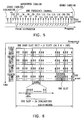
- a total of 192 subcarriers arranged in the frequency axis direction (hereinafter referred to as one band slot unit) are arranged in four rows in the time axis direction (these four rows will hereinafter be referred to as the first through the fourth time slot units), and these 192 ⁇ 4 subcarriers constitute a data block which is used as a data unit.
- Symbol data are superposed on the phase differences between the subcarriers in this data block.
- the minimum unit constituting the data block is one slot consisting of twenty-four subcarriers arranged in the frequency axis direction, and one band slot unit is formed from eight slots. That is, since four time slot units are transmitted as a data block in the time axis direction, the entire data block is constituted by thirty-two slots (8 slots ⁇ 4 time slot units). Note that when ordinary voice data are transmitted, the amount of data is small compared with image data and therefore multicarrier communication is performed in the unit of one slot which is the minimum unit of the data block.
- the bandwidth between the subcarriers is 5 KHz
- the bandwidth of the entire data block is 960 KHz. Therefore, if it is assumed that the bandwidth of the entire system is 30 MHz, the number of lines that can be simultaneously provided with users will be about 31 lines. Note that the transmission time in one time slot unit is 200 ⁇ sec.
- the leftmost subcarrier C0 of 192 subcarriers C0 to C191 in the first time slot unit is first employed as a reference carrier, and based on the phase difference between the subcarrier C0 and the subcarrier C1 adjacent right, symbol data are modulated. That is, a so-called differential modulation process in the frequency axis direction (lateral direction) is performed.
- symbol data are modulated based on the phase difference between adjacent subcarriers in the time axis direction (lateral direction) of 192 subcarriers C192 to C384 in the second time slot unit and 192 subcarriers C0 to C191 in the first time slot unit. That is, a so-called differential modulation process in the time axis direction is performed.
- symbol data are modulated based on the phase difference between adjacent subcarriers in the time axis direction.
- This differential modulation process in the time axis direction is weak to the flat fading and frequency-selective fading which will occur due to time variations during high-speed movement, so data degradation will arise.
- this process is a differential modulation in the time axis direction, data degradation will not occur when the moving speed is lower than the transmission time for one time slot unit or in the communication environment where there is no movement.
- the differential modulation process in the time axis direction is independent of the frequency axis direction and therefore has a characteristic that is robust to the flat fading and frequency-selective fading caused by delayed waveforms.
- both the differential modulation process in the frequency axis direction and the differential modulation process in the time axis direction are performed at a ratio according to the communication environment where the portable telephone of the cellular system is used. With this, in the state in which data degradation arising on the transmission path has been reduced, transmission is performed. At the receiving side, as with the transmitting side, the differential modulation processes in the frequency axis and time axis directions are performed. With this, since the data degradation caused by the fading on the transmission path is reduced, data can be restored more accurately.
- the ratio that the differential modulation process in the frequency axis direction is performed is increased in the communication environment where high-speed movement is primarily performed, and the ratio is increased in the communication environment where the influence of the frequency-selective fading caused by waveforms delayed by reflections from buildings or mountains is large (modulation pattern shown in Fig. 7). Therefore, in the state in which data degradation during transmission has been minimized according to communication environment, transmission can been performed.
- the differential modulation process in the frequency axis direction is performed when the first time slot unit is processed, while the differential modulation process in the time axis direction is performed when the second time slot unit and the time slot unit thereafter are processed.
- the number of reference carriers can be reduced only to a single subcarrier C0. Therefore, since the wasteful reference carrier having no meaning as symbol data can be constituted by a single subcarrier C0, it becomes possible to enhance transmission efficiency in transmitting a data bit series which has a large amount of data.
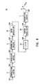
- reference numeral 20 generally denotes a transmitter, which performs a differential modulation process by the above-mentioned system.
- Data bit series S20 is first input to a convolution coding circuit 2.
- the convolution coding circuit 2 consists of a predetermined stage-number of shift registers and exclusive OR circuits.
- the convolution coding circuit 2 performs convolution coding on the input data bit series S20 and outputs the resulting coded bit series S21 to an interleave buffer 3.
- the interleave buffer 3 stores the coded bit series S21 in its internal storage region in sequence. If the coded bit series S21 is stored in the entire storage region (i.e., if the coded bit series S21 is accumulated a desired amount), then the coded bit series S21 will be interleaved. The resulting coded bit series S22 is output to a segmenting circuit 4.
- the interleave buffer 3 has a storage capacity equivalent to a plurality of slots so that the coded bit series S21 is dispersed to a plurality of transmission slots TX.
- the segmenting circuit 4 segments the coded bit series S22 every a predetermined number bits to allocate the coded bit series S22 to transmission slots TX.
- the resulting coded bit group S23 is output to a DQPSK modulation circuit 21 in sequence.
- the coded bit group S23 allocated to the transmission slots TX is equivalent to the data amount that is transmitted by one data block.
- the DQPSK modulation circuit 21 performs a DQPSK modulation process on the coded bit group S23 in accordance with a predetermined ratio at which the differential modulation processes in the frequency axis and time axis directions are performed and with a predetermined modulation pattern, thereby generating a transmission signal in which symbol data are represented by phase values.
- the predetermined ratio and modulation pattern are previously determined by a control section (not shown) .
- the DQPSK modulation circuit 21 performs a ⁇ /4 shift DQPSK modulation process (in which the maximum phase change is suppressed to ⁇ 3 ⁇ /4 by shifting the phase change in the previous symbol by ⁇ /4).
- the DQPSK modulation circuit 21 performs the differential modulation process in the frequency axis direction on the coded bit group S23, because symbol data are allocated to the phase differences between the subcarriers C0 to C191 in the first time slot unit in the data block.
- the DQPSK modulation circuit 21 also performs the differential modulation process in the time axis direction on the coded bit group S23, because symbol data are allocated to the phase differences between the subcarriers in the second time slot unit and the time slot units thereafter.
- the resulting data symbol group S24 is output to an inverse fast Fourier transformation (IFFT) circuit 22.
- IFFT inverse fast Fourier transformation
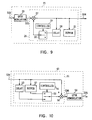
- the DQPSK modulation circuit 21 is constituted by a QPSK modulation circuit 25 and a differential modulation circuit 26.
- the QPSK modulation circuit 25 performs a QPSK modulation process on the code bit group S23 in sequence, thereby generating a transmission symbol stream D25 in which 2-bit data are mapped on a symbol. This stream is output to the multiplier 27 of the differential modulation circuit 26.
- the differential modulation circuit 26 inputs the transmission symbol prior to one symbol, obtained from the transmission symbol stream D25 through a delay circuit 28, to the multiplier 27 through a switch circuit 30 which is switched by a controller 29.
- the transmission symbol prior to one symbol and the currently input transmission symbol are multiplied by the multiplier 27.
- the differential modulation circuit 26 performs differential modulation on symbol data, based on the phase difference between the currently input transmission symbol and the transmission symbol prior to one symbol. This modulation process is reiterated for each of the 192 transmission symbols to generate symbol data group S24.
- the symbol data groups S24 are output to the IFFT circuit 22.
- the differential modulation circuit 26 inputs the 192 transmission symbols in the first time slot unit stored in the buffer 31 to the multiplier 27 one by one through the switch circuit 30, and multiplies the 192 transmission symbols in the first time slot unit and the currently input 192 transmission symbols in the second time slot unit, thereby performing the differential modulation process in the time axis direction.
- the resulting symbol data group S24 is output to the IFFT circuit 22.
- the differential modulation circuit 26 performs the differential modulation process in the time axis direction on the third time slot unit and the time slot unit thereafter in a similar manner.
- the resulting symbol data group S24 is output to the IFFT circuit 22.
- the IFFT circuit 22 performs an inverse fast Fourier process when all symbol data in the first time slot unit in the data symbol group S24 are input, thereby superposing the symbol data on each phase difference between the subcarriers C0 to C191. Likewise, the IFFT circuit 22 performs an inverse fast Fourier process when 192 symbol data in the second time slot unit or the time slot units thereafter are input, thereby superposing the symbol data of the data symbol group S24 on each phase difference between the subcarriers adjacent to each other in the time axis direction.
- the IFFT circuit 22 also performs a window process on the transmission signal S25 generated by performing the inverse Fourier transformation process. With this, an unnecessary spurious output is suppressed. Note that the window process can be realized by passing the transmission signal S25 through a cosine roll-off filter in the time axis direction.
- the transmission signal S25, generated by the IFFT circuit 22, is input to a random phase shift circuit 23.
- the random phase shift circuit 23 adds random phase values to the phases of a plurality of subcarriers forming the transmission signal S25, thereby making the phases of the plurality of subcarriers random.
- the random phase values are generated by a predetermined rule with an initial phase value as reference.
- the resulting transmission signal S26 is output to a subsequent transmitting circuit 7.
- the transmitting circuit 7 first performs a filtering process on the transmission signal S26, then performs a digital-analog conversion process on the transmission signal S26, and performs a frequency transformation process. As a result, a transmission signal S27 with a predetermined frequency channel is generated. After this generated signal has been amplified to a predetermined electric power, the amplified signal is transmitted through an antenna 8. Note that the transmitting circuit 7 performs a so-called frequency hopping (FH) process in which the frequency channel to be used for each data block is randomly changed based on a predetermined hopping pattern. With this process, the influence of an interference waveform caused by other communications is reduced.
- FH frequency hopping
- the transmitter 20 by performing the DQPSK modulation processes in the frequency axis and time axis directions on the coded bit group S23 at a predetermined ratio and then performing an inverse fast Fourier transformation process, symbol data are superposed on the phase differences between a plurality of subcarriers. After a predetermined transmission process has been performed, the processed symbol data are transmitted as a transmission signal S27.
- reference numeral 40 generally denotes a receiver.
- the receiver 40 is roughly constituted by an antenna 11, a receiving circuit 41, a fast Fourier transformation circuit (FFT) 42, a random phase inverse shift circuit 43, a demodulation circuit 44, a slot coupling circuit 15, a deinterleave buffer 16, and a Viterbi decoding circuit 17.
- the receiver 40 has almost the same constitution as the receiving circuit 10 shown in Fig. 3, except that the fast Fourier transformation circuit 42 and the random phase inverse shift circuit 43 are newly added instead of the transmission path estimating circuit 13 and that the processing contents of the receiving circuit 41 and demodulation circuit 44 are changed.
- the antenna 11 receives the transmission signal S27 transmitted from the transmitter 20, and this is input to the receiving circuit 41 as a received signal S11.
- the receiving circuit 41 amplifies the input received signal S31 and then performs a frequency transformation on the received signal S31, thereby taking out a base band signal.
- the receiving circuit performs a filtering process on the base band signal and then performs an analog-to-digital conversion process on the base band signal, thereby taking out a received signal S32. This signal is output to the fast Fourier transformation circuit (FFT) 42.
- FFT fast Fourier transformation circuit
- the fast Fourier transformation circuit 42 performs a window process on the input received signal S32, thereby taking out the signal components equivalent to the first time slot unit by an amount equivalent to a total of four time slot units. A Fourier transformation is performed on these signal components. With this, the fast Fourier transformation circuit 42 takes out the symbol data superposed on the phase differences between a plurality of subcarriers. The symbol data are output to the random phase inverse shift circuit 43 as a received signal S33.
- the random phase inverse shift circuit 43 returns the phase state of the received signal S33 to the original state by employing the same phase value as the transmitting side, and outputs the resulting received signal S34 to a subsequent demodulation circuit 44.
- the demodulation circuit 44 is constituted by a DQPSK demodulation circuit 45 and a weighting circuit 46, and outputs the received signal S34 to both the DQPSK demodulation circuit 45 and the weighting circuit 46.
- the DQPSK demodulation circuit 45 as with the transmitting side, performs the differential demodulation process in the frequency axis direction on the received signal S34 on which the differential modulation process in the frequency axis direction was performed, and also performs the differential demodulation process in the time axis direction on the received signal S34 on which the differential modulation process in the time axis direction was performed. This resulting received symbol S35 is output to the weighting circuit 46.
- the DQPSK demodulation circuit 45 is constituted by a differential demodulation circuit 51 and a QPSK demodulation circuit 52.
- the differential demodulation circuit 51 inputs the received signal S34 delayed by one symbol, which is obtained through a delay circuit 53 from the input received signal S34, to a multiplier 56 through a switch circuit 55 which is switched by a controller 54.
- the differential demodulation process in the frequency axis direction is performed to take out the received symbols S36 equivalent to the first time slot unit from the received signal S34.
- the received symbols S36 are output to the QPSK demodulation circuit 52.
- the differential modulation circuit 51 also inputs the symbols of the received signal S34 of the first time slot unit prior to one transmission time, stored in the buffer 57, to the multiplier 56 one by one through the switch circuit 55. By complex multiplying the input symbol and each symbol of the currently input received signal S34 of the second time slot unit, the differential demodulation process in the time axis direction is performed. The resulting received symbols S36 are output to the QPSK demodulation circuit 52. Furthermore, the differential demodulation circuit 51 likewise performs the differential demodulation process in the time axis direction on the third time slot unit and the time slot unit thereafter. The resulting received symbols S36 are output to the QPSK demodulation circuit 52.
- the QPSK demodulation circuit 52 performs a QPSK demodulation process on the received symbols S36 obtained by the differential demodulation processes in the frequency axis and time axis directions.
- the resulting received symbols S35 are output to the weighting circuit 46.
- the weighting circuit 46 computes reliability in the data block (which is the data unit of communication data) for each data block, based on the received signal S34, and also computes a weighting coefficient according to the reliability. And the weighting circuit 46 multiplies the weighting coefficient and the received symbol S35 together for each data block, thereby reflecting the data block reliability in the signal level of the received symbol S35. The resulting received symbols S37 are output to a slot coupling circuit 15.
- the weighting circuit 46 computes a mean value for computing reliability in a data block unit based on a large amount of sample data, whereby an error in the reliability can be reduced. Therefore, a weighting coefficient can be computed more accurately.
- the slot coupling circuit 15 is one which couples symbols S37 separately received in a data block unit so that they become a series signal. If the received symbols S37 are accumulated by an amount corresponding to the storage capacity of the deinterleave buffer 16 of the latter stage, then the received symbols S37 will be coupled together. The coupled received symbol group S38 is output to the deinterleave buffer 16.
- the deinterleave buffer 16 has a storage capacity equivalent to a plurality of slots.
- the deinterleave buffer 16 stores the received symbol group S38 in its internal storage region in sequence and then rearrange the order of the received symbol group S38 in the order opposite the rearrangement made by the interleave buffer 3 of the transmitter 20, thereby returning the arrangement to the original order.
- the resulting data bit stream S39 is output to a Viterbi decoding circuit 17.
- the Viterbi decoding circuit 17 consists of a soft judgment Viterbi decoding circuit.
- the Viterbi decoding circuit 17 performs maximum likelihood estimation on the input data bit stream S39, thereby restoring a data bit series 40 transmitted from the transmitting side.
- the weighting circuit 46 of the first stage has computed data block reliability and multiplied the received symbol S35 and a weighting coefficient representing the data block reliability. For this reason, the data bit stream 39 input to the Viterbi decoding circuit 17 has a signal level corresponding to the data block reliability.
- the Viterbi decoding circuit 17 performs maximum likelihood estimation even more accurately and is able to restore the data bit series S40 even more accurately.
- the transmitter 20 performs transmission by implementing both the differential modulation process in the frequency axis direction which is robust to the influence of flat fading or frequency-selective fading caused by time variations during high-speed movement and the differential modulation in the time axis direction which is robust to the influence of frequency-selective fading caused by delayed waveforms, at a ratio predetermined within one data block.
- the transmitter 20 can superpose symbol data on the phase differences in the frequency axis and time axis directions between subcarriers, whereby the transmission efficiency of communication data can be raised as the entire data block.
- the transmitter 20 can efficiently reduce data degradation resulting from fading caused on the transmission path.
- the differential modulation process in the frequency axis direction is performed on the first time slot unit of the data block, while the differential modulation process in the time axis direction is performed on the second time slot unit and the time slot units thereafter. Therefore, as in the case where the differential modulation process in the time axis direction is performed on the entire data block, all subcarriers in the first time slot unit are employed as reference carriers for the subcarriers in the second time slot unit, and in addition to this, the symbol data can also be superposed on the phase differences in the frequency axis direction between the subcarriers in the first time slot unit. Therefore, more symbol data can be transmitted as a whole of one data block.
- a symbol with phase 0 and amplitude 1 (which has no meaning as symbol data) is allocated to the reference carrier C0 in the first time slot unit, and based on this symbol with phase 0 and amplitude 1, symbol data is superposed on the phase difference with the symbol of the subcarrier C adjacent in the frequency direction. Also, symbol data is superposed on the phase difference in the time axis direction between the reference carrier C0 and the symbol of the subcarrier C192 in the second time slot unit. Therefore, if an unnecessary phase rotation occurs due to noise added to the symbol of the reference carrier C0, then an unnecessary phase offset will occur between adjacent subcarrier C1 and symbol of the subcarrier C192 and therefore data degradation will occur when the differential modulation process is performed.
- symbol data is superposed on the phase difference, so even if an unnecessary phase rotation occurs due to noise added to the symbol of the reference carrier C0, the subcarrier C1 and the symbol of the subcarrier C192 can be employed as a subsequent reference carrier if no phase rotation occurs between the subcarrier C1 and the symbol of the subcarrier C192.
- the receiver 40 receives the transmission signal S27 on which the differential modulation processes in the frequency axis and time axis directions were performed at a predetermined ratio according to communication environment, so that reception can be performed while in the state in which data degradation occurring on the transmission path has been reduced.
- the differential demodulation process in the frequency axis direction on the received signal S34 on which the differential modulation process in the frequency axis direction was performed at the transmitting side and also by performing the differential demodulation process in the time axis direction on the received signal S34 on which the differential modulation process in the time axis direction was performed, symbol data are restored. With this, the data bit series S40 can be restored more accurately.
- the receiver 40 by computing a weighting coefficient in order to reflect reliability in communication quality for every data block and then multiplying the weighting coefficient and the received symbol S35, even in the case where communication quality differs from data block to data block, the communication quality is reflected in the signal level by reliability, so that the data bit series S40 can be restored even more accurately because of the addition of reliability for every data block.
- both the differential modulation process in the frequency axis direction and the differential modulation process in the time axis direction are performed within one data block at a predetermined ratio according to communication environment at the transmitting side.
- the influence of fading caused by the transmission path can be reduced according to communication environment. Accordingly, a transmission signal in a state of less data degradation can be efficiently transmitted.
- the original data bit series can be restored more accurately by performing the differential demodulation processes in the frequency axis and time axis directions in the same manner as the transmitting side.
- the present invention is not limited to this but the differential modulation process in the frequency axis direction can be performed on any time slot unit.
- the data block which consists of four time slot units in time axis direction each constituting a band slot unit consisting of 192 subcarriers arranged in the frequency axis direction, is constituted as a data unit
- the present invention is not limited to this but the data block can be constituted by various numbers of subcarriers and time slot units.
- the differential modulation process in the frequency axis direction is performed on the first time slot unit and that the differential modulation process in the time axis direction is performed on the second through the fourth time slot units
- the present invention is not limited to this.
- the differential modulation process in the frequency axis direction and the differential modulation process in the time axis direction can be alternately performed.
- modulation patterns consisting of various combinations may be employed.
- the differential modulation processes in the frequency axis direction and in the time axis direction are alternately performed. Even under communication environment where only waveforms delayed by the multipath occur or communication environment which is used only at the time of high-speed movement, half of data can be restored without degradation.
- this modulation pattern can be employed as a cryptograph and therefore secrecy can be enhanced.
- weighting is performed in the unit of a data block
- the present invention is not limited to this.
- weighting can be performed in the unit of a slot (24 subcarriers) which is the data unit of voice data.
- a slot 24 subcarriers
- weighting can be finely performed in the unit of one slot which is the minimum unit of the data block.
- DQPSK modulation circuit 21 modulation means
- transmission signal S27 is generated and transmitted by the FFT circuit 22 and transmitting circuit 7 (transmission means)
- Modulation means employing various modulation methods, such as 8PSK or 16PSK, can be employed, so long as they are a method of superposing symbol data on a phase difference.
Landscapes
- Engineering & Computer Science (AREA)
- Computer Networks & Wireless Communication (AREA)
- Signal Processing (AREA)
- Digital Transmission Methods That Use Modulated Carrier Waves (AREA)
- Mobile Radio Communication Systems (AREA)
Applications Claiming Priority (2)
| Application Number | Priority Date | Filing Date | Title |
|---|---|---|---|
| JP301341/97 | 1997-10-31 | ||
| JP9301341A JPH11136180A (ja) | 1997-10-31 | 1997-10-31 | データ通信方法、送信装置及びセルラー無線通信システム |
Publications (1)
| Publication Number | Publication Date |
|---|---|
| EP0913972A2 true EP0913972A2 (de) | 1999-05-06 |
Family
ID=17895704
Family Applications (1)
| Application Number | Title | Priority Date | Filing Date |
|---|---|---|---|
| EP98120486A Withdrawn EP0913972A2 (de) | 1997-10-31 | 1998-10-29 | Mehrträger-Funkübertragungssystem |
Country Status (3)
| Country | Link |
|---|---|
| US (1) | US6456669B1 (de) |
| EP (1) | EP0913972A2 (de) |
| JP (1) | JPH11136180A (de) |
Cited By (5)
| Publication number | Priority date | Publication date | Assignee | Title |
|---|---|---|---|---|
| EP1085714A3 (de) * | 1999-09-13 | 2001-10-17 | Deutsches Zentrum für Luft- und Raumfahrt e.V. | Differentielle Demodulation in zwei oder mehreren Dimensionen |
| WO2003049474A1 (en) | 2001-12-04 | 2003-06-12 | Sumitomo Electric Industries, Ltd. | Mobile body communication apparatus |
| AU767901B2 (en) * | 2000-11-06 | 2003-11-27 | Ntt Docomo, Inc. | Transmitter, transmitting method, receiver, and receiving method for MC-CDMA communication system |
| WO2004075502A3 (en) * | 2003-02-19 | 2005-01-27 | Matsushita Electric Industrial Co Ltd | Receiving apparatus and method for digital multi-carrier transmission |
| US10772082B2 (en) | 2007-12-20 | 2020-09-08 | Optis Wireless Technology, Llc | Control channel signaling using a common signaling field for transport format, redundancy version, and new data indicator |
Families Citing this family (12)
| Publication number | Priority date | Publication date | Assignee | Title |
|---|---|---|---|---|
| WO2000003508A1 (fr) * | 1998-07-13 | 2000-01-20 | Sony Corporation | Procede de communication, emetteur, et recepteur |
| US7143013B2 (en) * | 1999-11-04 | 2006-11-28 | Verticalband, Limited | Reliable symbols as a means of improving the performance of information transmission systems |
| US7110923B2 (en) * | 1999-11-04 | 2006-09-19 | Verticalband, Limited | Fast, blind equalization techniques using reliable symbols |
| US7085691B2 (en) * | 1999-11-04 | 2006-08-01 | Verticalband, Limited | Reliable symbols as a means of improving the performance of information transmission systems |
| US6961369B1 (en) * | 1999-11-09 | 2005-11-01 | Aware, Inc. | System and method for scrambling the phase of the carriers in a multicarrier communications system |
| FI20001513A7 (fi) * | 2000-06-26 | 2001-12-27 | Nokia Corp | Menetelmä tiedonsiirron laadun parantamiseksi |
| US6754284B2 (en) * | 2002-08-22 | 2004-06-22 | Motorola, Inc. | Method and apparatus for minima enlargement |
| JP2005079905A (ja) * | 2003-08-29 | 2005-03-24 | Toshiba Corp | 無線システム、送信装置、受信装置、および通信方法 |
| WO2005081437A1 (en) * | 2004-02-17 | 2005-09-01 | Huawei Technologies Co., Ltd. | Multiplexing scheme in a communication system |
| RU2349051C2 (ru) * | 2004-11-16 | 2009-03-10 | Самсунг Электроникс Ко., Лтд. | Устройство и способ обработки цифрового сигнала в системе беспроводной связи ofdma |
| RU2527748C2 (ru) * | 2005-10-27 | 2014-09-10 | Квэлкомм Инкорпорейтед | Предварительное кодирование для зависящего от сегмента планирования в беспроводных системах связи |
| WO2008078919A2 (en) * | 2006-12-22 | 2008-07-03 | Lg Electronics Inc. | Methods for sequence generation and transmission based on time and frequency domain transmission unit in a mobile communication system |
Family Cites Families (10)
| Publication number | Priority date | Publication date | Assignee | Title |
|---|---|---|---|---|
| NL7213388A (de) * | 1971-12-01 | 1974-04-08 | ||
| US4943980A (en) * | 1989-05-02 | 1990-07-24 | Intelligent Modem Corporation | Multi-carrier high speed modem |
| JPH0422225A (ja) | 1990-05-17 | 1992-01-27 | Sony Corp | 通信方式 |
| US5519730A (en) * | 1990-06-12 | 1996-05-21 | Jasper; Steven C. | Communication signal having a time domain pilot component |
| JPH04177946A (ja) | 1990-11-09 | 1992-06-25 | Sony Corp | デジタル復調装置 |
| JPH0746217A (ja) * | 1993-07-26 | 1995-02-14 | Sony Corp | ディジタル復調装置 |
| US5444697A (en) * | 1993-08-11 | 1995-08-22 | The University Of British Columbia | Method and apparatus for frame synchronization in mobile OFDM data communication |
| JP3145003B2 (ja) * | 1995-03-23 | 2001-03-12 | 株式会社東芝 | 直交周波数分割多重伝送方式とその送信装置および受信装置 |
| JPH10308717A (ja) * | 1997-05-02 | 1998-11-17 | Sony Corp | 受信装置および受信方法 |
| JPH1117760A (ja) * | 1997-06-24 | 1999-01-22 | Sony Corp | 受信装置及び送受信装置並びに通信方法 |
-
1997
- 1997-10-31 JP JP9301341A patent/JPH11136180A/ja active Pending
-
1998
- 1998-10-23 US US09/178,163 patent/US6456669B1/en not_active Expired - Fee Related
- 1998-10-29 EP EP98120486A patent/EP0913972A2/de not_active Withdrawn
Cited By (9)
| Publication number | Priority date | Publication date | Assignee | Title |
|---|---|---|---|---|
| EP1085714A3 (de) * | 1999-09-13 | 2001-10-17 | Deutsches Zentrum für Luft- und Raumfahrt e.V. | Differentielle Demodulation in zwei oder mehreren Dimensionen |
| AU767901B2 (en) * | 2000-11-06 | 2003-11-27 | Ntt Docomo, Inc. | Transmitter, transmitting method, receiver, and receiving method for MC-CDMA communication system |
| CN100405757C (zh) * | 2000-11-06 | 2008-07-23 | 株式会社Ntt都科摩 | 多路载波通讯系统的发送技术和方法及接收技术和方法 |
| WO2003049474A1 (en) | 2001-12-04 | 2003-06-12 | Sumitomo Electric Industries, Ltd. | Mobile body communication apparatus |
| EP1463355A4 (de) * | 2001-12-04 | 2010-04-14 | Sumitomo Electric Industries | Mobilkörperkommunikationsvorrichtung |
| WO2004075502A3 (en) * | 2003-02-19 | 2005-01-27 | Matsushita Electric Industrial Co Ltd | Receiving apparatus and method for digital multi-carrier transmission |
| US6944232B2 (en) | 2003-02-19 | 2005-09-13 | Matsushita Electric Industrial Co. Ltd. | Receiving apparatus and method for digital multi-carrier transmission |
| US10772082B2 (en) | 2007-12-20 | 2020-09-08 | Optis Wireless Technology, Llc | Control channel signaling using a common signaling field for transport format, redundancy version, and new data indicator |
| US11477767B2 (en) | 2007-12-20 | 2022-10-18 | Optis Wireless Technology, Llc | Control channel signaling using a common signaling field for transport format, redundancy version, and new data indicator |
Also Published As
| Publication number | Publication date |
|---|---|
| US6456669B1 (en) | 2002-09-24 |
| JPH11136180A (ja) | 1999-05-21 |
Similar Documents
| Publication | Publication Date | Title |
|---|---|---|
| US6456669B1 (en) | Data communication method, transmitter, and cellular radio communication system | |
| US6243423B1 (en) | Receiver, transmitter-receiver, and communication method | |
| US7453794B2 (en) | Channel estimation and synchronization with preamble using polyphase code | |
| US7949061B2 (en) | Scattered pilot pattern and channel estimation method for MIMO-OFDM systems | |
| US20050201326A1 (en) | Systems and methods for wireless communication over a wide bandwidth channel using a plurality of sub-channels | |
| US6574283B1 (en) | Communication method, transmission and reception apparatuses, and cellular radio communication system | |
| US20050094613A1 (en) | Apparatus and method for transmitting/receiving a pilot signal for distinguishing a base station in a communication system using an OFDM scheme | |
| EP1283614A1 (de) | Kanalschätzung in einem Mehrträger-Übertragungssystem mit Sende-Diversity | |
| US20090175162A1 (en) | Method of OFDM communication using superposition coding | |
| US20080107199A1 (en) | Systems and methods for recovering bandwidth in a wireless communication network | |
| KR100584439B1 (ko) | 다중 안테나를 사용하는 직교주파수분할다중 시스템에서간섭신호 제거 장치 및 방법 | |
| US20030016622A1 (en) | Dual domain differential encoder/decoder | |
| JP4633054B2 (ja) | 直交周波数分割多重変調を使用して超広帯域信号を通信する方法および送信機 | |
| KR20030038270A (ko) | 직교주파수분할다중 방식의 이동통신시스템에서시공간-주파수 부호화/복호화 장치 및 방법 | |
| US20050207505A1 (en) | Systems and methods for recovering bandwidth in a wireless communication network | |
| US20050157782A1 (en) | Systems and methods for transmitting data in a wireless communication network | |
| KR100769671B1 (ko) | Mb-ofdm 송수신장치 및 그 신호처리 방법 | |
| JP4538052B2 (ja) | Ofdm信号の処理方法及びofdm送信機 | |
| JP4806766B2 (ja) | 無線通信方法、受信状況推定方法、送信装置、および、受信装置 | |
| KR101378695B1 (ko) | 통신 시스템에서의 훈련 시퀀스 코드 생성 방법 및 장치 | |
| US20050152483A1 (en) | Systems and methods for implementing path diversity in a wireless communication network | |
| JP2000092022A (ja) | マルチキャリアディジタル変調伝送装置 | |
| KR20000000275A (ko) | 주파수 도약 - 직교 주파수 분할 다중화 방식 및 장치 | |
| Tomba et al. | An OFDM/SFH-CDMA transmission scheme for the uplink |
Legal Events
| Date | Code | Title | Description |
|---|---|---|---|
| PUAI | Public reference made under article 153(3) epc to a published international application that has entered the european phase |
Free format text: ORIGINAL CODE: 0009012 |
|
| AK | Designated contracting states |
Kind code of ref document: A2 Designated state(s): AT BE CH CY DE DK ES FI FR GB GR IE IT LI LU MC NL PT SE |
|
| AX | Request for extension of the european patent |
Free format text: AL;LT;LV;MK;RO;SI |
|
| STAA | Information on the status of an ep patent application or granted ep patent |
Free format text: STATUS: THE APPLICATION IS DEEMED TO BE WITHDRAWN |
|
| 18D | Application deemed to be withdrawn |
Effective date: 20030503 |