EP0914677B1 - Schichtaufbau mit einer ferroelektrischen schicht und herstellverfahren - Google Patents
Schichtaufbau mit einer ferroelektrischen schicht und herstellverfahren Download PDFInfo
- Publication number
- EP0914677B1 EP0914677B1 EP97932728A EP97932728A EP0914677B1 EP 0914677 B1 EP0914677 B1 EP 0914677B1 EP 97932728 A EP97932728 A EP 97932728A EP 97932728 A EP97932728 A EP 97932728A EP 0914677 B1 EP0914677 B1 EP 0914677B1
- Authority
- EP
- European Patent Office
- Prior art keywords
- layer
- ferroelectric
- substrate
- platinum
- layer structure
- Prior art date
- Legal status (The legal status is an assumption and is not a legal conclusion. Google has not performed a legal analysis and makes no representation as to the accuracy of the status listed.)
- Expired - Lifetime
Links
Images

Classifications
-
- H—ELECTRICITY
- H10—SEMICONDUCTOR DEVICES; ELECTRIC SOLID-STATE DEVICES NOT OTHERWISE PROVIDED FOR
- H10B—ELECTRONIC MEMORY DEVICES
- H10B53/00—Ferroelectric RAM [FeRAM] devices comprising ferroelectric memory capacitors
-
- H—ELECTRICITY
- H10—SEMICONDUCTOR DEVICES; ELECTRIC SOLID-STATE DEVICES NOT OTHERWISE PROVIDED FOR
- H10D—INORGANIC ELECTRIC SEMICONDUCTOR DEVICES
- H10D1/00—Resistors, capacitors or inductors
- H10D1/60—Capacitors
- H10D1/68—Capacitors having no potential barriers
- H10D1/682—Capacitors having no potential barriers having dielectrics comprising perovskite structures
Definitions
- Ferroelectric layers are used in components, the dielectric, pyroelectric and piezoelectric Properties of ferroelectrics can be used.
- components with ferroelectric layers for example Capacitors, pyrodetectors, piezo actuators or semiconductor memories, the ferroelectric layers in the latter both as a dielectric and as a storage medium under Utilization of the hysteresis effect used in the polarization can be.
- EP 0 698 918 A describes a microelectronic one Layer structure known that consists of an oxidizable Substrate, an electrode and a dielectric with high Dielectric constant exists. Between the electrode and the An insulating layer is arranged on the substrate.
- the insulation layer for example made of a precious metal insulator alloy exists and must be electrically conductive, intends the task of diffusion of oxygen on all things restrict the surface of the substrate.
- Electrode is special as electrode material platinum suitable because it is the deposition conditions of the ferroelectric Layer at high temperatures and in oxygen The atmosphere survives undamaged and does not diffuse into the ferroelectric layer, which leads to a changed Composition and thus changed properties could lead.
- titanium-containing adhesion promoter layers have a number of disadvantages which lead to a deterioration in the electrical properties of ferroelectric capacitors and, in general, of ferroelectric components.
- Good ferroelectric properties are only obtained with ferroelectrics containing crystalline oxides, which are produced at elevated temperatures in an oxygen-containing atmosphere.
- a diffusion of titanium into the platinum and then an oxidation of the titanium to titanium oxide TiO 2 is observed.
- This is associated with a relatively high volume expansion, which leads to the formation of so-called hillocks on the surface of the platinum electrode.
- These irregularities in the structure continue in a ferroelectric layer applied there, leading to an unfavorable morphology and thus to unfavorable electrical and ferroelectric properties.
- the structural unevenness of the platinum electrode is so large that there is a short circuit in the ferroelectric component and thus a total failure of the component.
- ferroelectric layer very good adhesion has and on the other hand with a ferroelectric layer very good surface morphology results.
- the surface of the ferroelectric layer is free of hillocks and points opposite a structure with an intermediate layer containing titanium more regular, more homogeneous grain structure.
- a ferroelectric Layer with a more homogeneous structure shows better ferroelectric Properties, is easier to polarize and enables a higher permanent degree of polarization than a ferroelectric layer with a more inhomogeneous structure.
- ferroelectric layer With the layer structure according to the invention and the achieved thereby homogeneous surface morphology of ferroelectric It is possible to convert the ferroelectric layer into ferroelectric To make components thinner than before known. Even with thin ferroelectric layers no short circuit feared due to structural unevenness become. It is also possible with the invention to use ferroelectric Multilayer components, for example capacitors in the To produce multilayer construction in a simple manner without the structural unevenness of the individual layers increases with increasing Potentiate the number of layers in the stack. On ferroelectric capacitor with an inventive Layer construction can be done with thinner ferroelectric Produce shift and thus with higher capacity than with a known layer structure.
- An intermediate layer made of aluminum oxide leads to all conventional ones Substrate materials for improved adhesion, especially in the case of substrates whose surfaces are silicon oxide or include silicon nitride.
- pyrodetectors over a silicon nitride comprehensive membrane layer are built advantageously realized with the invention.
- the substrate temperature is, for example, from 200 to 300 ° C set.
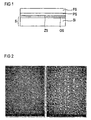
- FIG. 1 Any substrate, for example silicate glass or a silicon wafer Si, is used as the substrate S.
- This can comprise a surface layer OS made of silicon oxide SiO 2 or made of silicon nitride Si 3 N 4 .
- the thickness of this surface layer OS is of no importance for the adhesion and the morphology of the layers to be applied over it.
- the intermediate layer ZS is applied in a thickness of 10 to approximately 120 nm above the surface layer OS, for example by sputtering Al 2 O 3 at a substrate temperature of 100 ° to approximately 300 ° C.
- the platinum layer PS is applied, preferably also by sputtering at a substrate temperature of at least 100 ° to approx. 300 ° C.
- the use of the layer structure becomes the platinum layer PS applied in a suitable layer thickness, in but in all cases with the smallest possible layer thickness of for example 0.1 to 0.5 ⁇ m.
- the ferroelectric layer FS applied over it exists from a ferroelectric material, preferably from the Class of the titanate containing lead, which still has various supplements from the class of alkaline earth metals or zirconium can have. Best known representative of this with perovskite structure producible ferroelectric materials Lead zirconate titanate (PZT).
- PZT Lead zirconate titanate
- the thickness of the ferroelectric layer FS is of no importance. For ferroelectric components there is a layer thickness the ferroelectric layer from 200 nm to approx. 2 ⁇ m sufficient.
- FIG. 2 shows the surface structure in a SEM image the ferroelectric layer of the layer structure according to the invention in two resolutions.
- the surface structure in FIG. 3 is one ferroelectric layer of a known layer structure with a titanium-containing intermediate layer is shown as an SEM image.
- the ferroelectric Layer of the layer structure according to the invention ( Figure 2) a more homogeneous grain structure and no structural distortions (Hillocks) on.
- the surface structure of the known layer structure ( Figure 3), however, is clearly inhomogeneous and at the same time shows some hillocks in the form of special large grains protruding from the surface, evenness severely affect the surface.
Landscapes
- Semiconductor Integrated Circuits (AREA)
- Semiconductor Memories (AREA)
- Formation Of Insulating Films (AREA)
- Insulating Bodies (AREA)
- Other Surface Treatments For Metallic Materials (AREA)
- Fixed Capacitors And Capacitor Manufacturing Machines (AREA)
Abstract
Description
- Figur 1
- zeigt einen erfindungsgemäßen Schichtaufbau im schematischen Querschnitt.
- Figur 2
- zeigt die REM-Aufnahme von der Oberfläche eines erfindungsgemäßen Schichtaufbaus und
- Figur 3
- zeigt die Oberfläche eines aus dem Stand der Technik bekannten Schichtaufbaus mit titanhaltiger Zwischenschicht.
Claims (10)
- Schichtaufbau mit zumindestbei dem zwischen Substrat (S) und Platinschicht (PS) eine Zwischenschicht (ZS) aus amorphem Al2O3 angeordnet ist.einem Substrat (S)einer Platinschicht (PS)einer auf der Platinschicht (PS) angeordneten ferroelektrischen Schicht (FS)
- Schichtaufbau nach Anspruch 1,
bei dem die Oberfläche (OS) des Substrats (S) Siliziumdioxid umfaßt. - Schichtaufbau nach Anspruch 1 oder 2,
bei dem das Substrat (S) monokristallines Silizium mit einer Oberflächenschicht (OS) aus Siliziumdioxid umfaßt. - Schichtaufbau nach einem der Ansprüche 1 bis 3,
bei dem die Zwischenschicht (ZS) eine Schichtdicke von 10 bis ca.1000 nm besitzt. - Schichtaufbau nach einem der Ansprüche 1 bis 4,
bei dem die ferroelektrische Schicht (FS) aus dem Stoffsystem Pb(Zr,Ti)O3 ausgewählt ist. - Verfahren zur Herstellung eines Schichtaufbaus mit einem Substrat (S), einer Platinschicht (PS) und einer auf der Platinschicht angeordneten ferroelektrischen Schicht (FS), bei dem zwischen Substrat und Platinschicht eine Zwischenschicht (ZS) aus Al2O3 in einem Dünnschichtverfahren abgeschieden wird.
- Verfahren nach Anspruch 6,
bei dem die Zwischenschicht (ZS) bei einer Substrattemperatur von 100 bis 300°C abgeschieden wird. - Verfahren nach Anspruch 6 oder 7,
bei dem die ferroelektrischen Schicht (FS) bei einer Substrattemperatur von zumindest 450°C in einem Sauerstoff haltigen Plasma abgeschieden wird. - Verfahren nach einem der Ansprüche 6 bis 8,
bei dem die Platinschicht (PS) bei einer Substrattemperatur von 100 bis 300°C abgeschieden wird. - Verwendung eines Schichtaufbaus nach einem der Ansprüche 1 bis 5 zur Herstellung ferroelektrischer Dünnschichtbauelemente, wie Pyrodetektoren, Kondensatoren oder Speicher.
Applications Claiming Priority (3)
| Application Number | Priority Date | Filing Date | Title |
|---|---|---|---|
| DE19630110 | 1996-07-25 | ||
| DE19630110A DE19630110C2 (de) | 1996-07-25 | 1996-07-25 | Schichtaufbau mit einer ferroelektrischen Schicht und Herstellverfahren |
| PCT/DE1997/001396 WO1998005062A1 (de) | 1996-07-25 | 1997-07-02 | Schichtaufbau mit einer ferroelektrischen schicht und herstellverfahren |
Publications (2)
| Publication Number | Publication Date |
|---|---|
| EP0914677A1 EP0914677A1 (de) | 1999-05-12 |
| EP0914677B1 true EP0914677B1 (de) | 2002-11-13 |
Family
ID=7800872
Family Applications (1)
| Application Number | Title | Priority Date | Filing Date |
|---|---|---|---|
| EP97932728A Expired - Lifetime EP0914677B1 (de) | 1996-07-25 | 1997-07-02 | Schichtaufbau mit einer ferroelektrischen schicht und herstellverfahren |
Country Status (6)
| Country | Link |
|---|---|
| US (1) | US6139971A (de) |
| EP (1) | EP0914677B1 (de) |
| JP (1) | JP2011155271A (de) |
| DE (2) | DE19630110C2 (de) |
| TW (1) | TW362225B (de) |
| WO (1) | WO1998005062A1 (de) |
Families Citing this family (11)
| Publication number | Priority date | Publication date | Assignee | Title |
|---|---|---|---|---|
| DE10207130B4 (de) * | 2002-02-20 | 2007-09-27 | Infineon Technologies Ag | Verfahren zur Herstellung eines Bauelements sowie Bauelement mit einer Edelmetallschicht, einer Edelmetallsilizidschicht und einer oxidierten Silizidschicht |
| JP4601896B2 (ja) | 2002-10-30 | 2010-12-22 | 富士通セミコンダクター株式会社 | 半導体装置及びその製造方法 |
| JP2004281742A (ja) * | 2003-03-17 | 2004-10-07 | Japan Science & Technology Agency | 半導体素子、半導体センサーおよび半導体記憶素子 |
| JP4102345B2 (ja) * | 2003-08-25 | 2008-06-18 | 三星電子株式会社 | 強誘電膜を含む記録媒体、それを用いた不揮発性メモリ素子、および、その不揮発性メモリ素子のデータ記録/再生方法 |
| US7199002B2 (en) * | 2003-08-29 | 2007-04-03 | Infineon Technologies Ag | Process for fabrication of a ferroelectric capacitor |
| JP2005217044A (ja) | 2004-01-28 | 2005-08-11 | Fujitsu Ltd | 半導体装置及びその製造方法 |
| WO2008088727A2 (en) | 2007-01-12 | 2008-07-24 | Concert Pharmaceuticals, Inc. | Endothelin receptor antagonists |
| US8080549B2 (en) * | 2007-01-12 | 2011-12-20 | Concert Pharmaceuticals, Inc. | Endothelin receptor antagonists |
| US9349392B1 (en) | 2012-05-24 | 2016-05-24 | Western Digital (Fremont), Llc | Methods for improving adhesion on dielectric substrates |
| US10199266B2 (en) | 2016-12-26 | 2019-02-05 | Intel Corporation | Integrated circuit interconnect structure having metal oxide adhesive layer |
| US11121139B2 (en) * | 2017-11-16 | 2021-09-14 | International Business Machines Corporation | Hafnium oxide and zirconium oxide based ferroelectric devices with textured iridium bottom electrodes |
Family Cites Families (6)
| Publication number | Priority date | Publication date | Assignee | Title |
|---|---|---|---|---|
| US5212620A (en) * | 1992-03-03 | 1993-05-18 | Radiant Technologies | Method for isolating SiO2 layers from PZT, PLZT, and platinum layers |
| DE4328067C1 (de) * | 1993-08-20 | 1994-03-31 | Siemens Ag | Verfahren zum Aufbringen von metallischen Schichten auf einem nichtmetallischen Substrat unter Einsatz eines Haftvermittlers |
| JP3197782B2 (ja) * | 1994-04-29 | 2001-08-13 | インターナショナル・ビジネス・マシーンズ・コーポレ−ション | 半導体集積回路コンデンサおよびその電極構造 |
| US5622893A (en) * | 1994-08-01 | 1997-04-22 | Texas Instruments Incorporated | Method of forming conductive noble-metal-insulator-alloy barrier layer for high-dielectric-constant material electrodes |
| US5554564A (en) * | 1994-08-01 | 1996-09-10 | Texas Instruments Incorporated | Pre-oxidizing high-dielectric-constant material electrodes |
| US5654222A (en) * | 1995-05-17 | 1997-08-05 | Micron Technology, Inc. | Method for forming a capacitor with electrically interconnected construction |
-
1996
- 1996-07-25 DE DE19630110A patent/DE19630110C2/de not_active Expired - Lifetime
-
1997
- 1997-07-02 US US09/214,809 patent/US6139971A/en not_active Expired - Lifetime
- 1997-07-02 WO PCT/DE1997/001396 patent/WO1998005062A1/de not_active Ceased
- 1997-07-02 DE DE59708725T patent/DE59708725D1/de not_active Expired - Lifetime
- 1997-07-02 EP EP97932728A patent/EP0914677B1/de not_active Expired - Lifetime
- 1997-07-10 TW TW086109722A patent/TW362225B/zh active
-
2011
- 2011-03-02 JP JP2011044725A patent/JP2011155271A/ja active Pending
Also Published As
| Publication number | Publication date |
|---|---|
| JP2011155271A (ja) | 2011-08-11 |
| DE19630110C2 (de) | 1998-11-19 |
| EP0914677A1 (de) | 1999-05-12 |
| JP2000515329A (ja) | 2000-11-14 |
| DE59708725D1 (de) | 2002-12-19 |
| JP4746161B2 (ja) | 2011-08-10 |
| TW362225B (en) | 1999-06-21 |
| WO1998005062A1 (de) | 1998-02-05 |
| DE19630110A1 (de) | 1998-01-29 |
| US6139971A (en) | 2000-10-31 |
Similar Documents
| Publication | Publication Date | Title |
|---|---|---|
| DE69633423T2 (de) | Verfahren zur Herstellung eines mit einer dünnen ferroelektrischen Schicht überdeckten Substrats | |
| DE69513782T2 (de) | Dielektrischer Dünnfilm aus Barium und/oder Strontium-Titanat mit Erbium und Herstellungsverfahren | |
| DE69805865T2 (de) | Herstellungsverfahren von Platinschichten mit gesteuerter bevorzugter Orientierung unter Verwendung von Stickstoff | |
| DE69404354T2 (de) | Verbesserte Elektroden-Zwischenschicht für Materialien mit hohen dielektrisches Konstante | |
| DE19518044C2 (de) | Verfahren zur Herstellung und Anordnung von Speicherkondensatoren unter Verwendung von Materialien mit hoher Dielektrizitätskonstante | |
| DE60035311T2 (de) | Ferroelektrische Struktur aus Bleigermanat mit mehrschichtiger Elektrode | |
| EP0914677B1 (de) | Schichtaufbau mit einer ferroelektrischen schicht und herstellverfahren | |
| DE19649670C2 (de) | Verfahren zur Herstellung eines Kondensators einer Halbleitervorrichtung und auf diese Weise hergestellter Kondensator | |
| DE102020115315B4 (de) | Piezoelektrische Baugruppe und Prozess zum Bilden einer piezoelektrischen Baugruppe | |
| WO2000013224A1 (de) | Mikroelektronische struktur, verfahren zu deren herstellung und deren verwendung in einer speicherzelle | |
| EP1149421B1 (de) | Femfet-vorrichtung und verfahren zu deren herstellung | |
| EP0676384B1 (de) | Perowskithaltiger Verbundwerkstoff, Verfahren zu seiner Herstellung, elektronisches Bauelement und Modul | |
| DE19841402B4 (de) | Verfahren zur Herstellung eines Kondensators eines Halbleiterbauelementes | |
| EP1301948B1 (de) | Halbleiterbauelement mit einer piezo- oder pyroelektrischen schicht und dessen herstellungsverfahren | |
| EP1113488A2 (de) | Verfahren zum Herstellen einer strukturierten metalloxidhaltigen Schicht | |
| EP1111083B1 (de) | Verfahren zur Herstellung einer strukturierten Metallschicht | |
| EP1138065A1 (de) | Verfahren zum herstellen einer strukturierten metalloxidhaltigen schicht | |
| DE10161286A1 (de) | Integriertes Halbleiterprodukt mit Metall-Isolator-Metall-Kondensator | |
| DE10009762B4 (de) | Herstellungsverfahren für einen Speicherkondensator mit einem Dielektrikum auf der Basis von Strontium-Wismut-Tantalat | |
| DE102024115938B4 (de) | Mehrschichtaufbau und Verfahren zur Herstellung eines Mehrschichtaufbaus | |
| DE102024115435B3 (de) | Mehrschichtaufbau und Verfahren zur Herstellung eines Mehrschichtaufbaus | |
| DE102025115265A1 (de) | Mehrschichtaufbau und Verfahren zur Herstellung eines Mehrschichtaufbaus | |
| WO2000028584A1 (de) | Verfahren zum herstellen einer strukturierten metalloxidhaltigen schicht | |
| DE10103529B4 (de) | Ferroelektrischer Kondensator, Verfahren zur Herstellung und Verwendung des Kondensators | |
| DE69632890T2 (de) | Mit einer dünnen ferroelektrischen Schicht überdecktes Substrat, Verfahren zu seiner Herstellung und dieses enthaltendes Kondensatorstrukturelement |
Legal Events
| Date | Code | Title | Description |
|---|---|---|---|
| PUAI | Public reference made under article 153(3) epc to a published international application that has entered the european phase |
Free format text: ORIGINAL CODE: 0009012 |
|
| 17P | Request for examination filed |
Effective date: 19990120 |
|
| AK | Designated contracting states |
Kind code of ref document: A1 Designated state(s): CH DE FR GB IT LI |
|
| GRAG | Despatch of communication of intention to grant |
Free format text: ORIGINAL CODE: EPIDOS AGRA |
|
| GRAG | Despatch of communication of intention to grant |
Free format text: ORIGINAL CODE: EPIDOS AGRA |
|
| GRAH | Despatch of communication of intention to grant a patent |
Free format text: ORIGINAL CODE: EPIDOS IGRA |
|
| 17Q | First examination report despatched |
Effective date: 20020517 |
|
| GRAH | Despatch of communication of intention to grant a patent |
Free format text: ORIGINAL CODE: EPIDOS IGRA |
|
| GRAA | (expected) grant |
Free format text: ORIGINAL CODE: 0009210 |
|
| AK | Designated contracting states |
Kind code of ref document: B1 Designated state(s): CH DE FR GB IT LI |
|
| REG | Reference to a national code |
Ref country code: GB Ref legal event code: FG4D Free format text: NOT ENGLISH |
|
| REG | Reference to a national code |
Ref country code: CH Ref legal event code: NV Representative=s name: SIEMENS SCHWEIZ AG Ref country code: CH Ref legal event code: EP |
|
| REF | Corresponds to: |
Ref document number: 59708725 Country of ref document: DE Date of ref document: 20021219 |
|
| GBT | Gb: translation of ep patent filed (gb section 77(6)(a)/1977) |
Effective date: 20030210 |
|
| ET | Fr: translation filed | ||
| PLBE | No opposition filed within time limit |
Free format text: ORIGINAL CODE: 0009261 |
|
| STAA | Information on the status of an ep patent application or granted ep patent |
Free format text: STATUS: NO OPPOSITION FILED WITHIN TIME LIMIT |
|
| 26N | No opposition filed |
Effective date: 20030814 |
|
| REG | Reference to a national code |
Ref country code: CH Ref legal event code: PUE Owner name: PYREOS LTD. Free format text: SIEMENS AKTIENGESELLSCHAFT#WITTELSBACHERPLATZ 2#80333 MUENCHEN (DE) -TRANSFER TO- PYREOS LTD.#WEST MAINS ROAD#EDINBURGH EH9 3JF (GB) Ref country code: CH Ref legal event code: NV Representative=s name: BRAUNPAT BRAUN EDER AG |
|
| REG | Reference to a national code |
Ref country code: GB Ref legal event code: 732E |
|
| REG | Reference to a national code |
Ref country code: FR Ref legal event code: TP |
|
| REG | Reference to a national code |
Ref country code: FR Ref legal event code: PLFP Year of fee payment: 20 |
|
| PGFP | Annual fee paid to national office [announced via postgrant information from national office to epo] |
Ref country code: GB Payment date: 20160722 Year of fee payment: 20 Ref country code: IT Payment date: 20160728 Year of fee payment: 20 Ref country code: DE Payment date: 20160720 Year of fee payment: 20 Ref country code: CH Payment date: 20160726 Year of fee payment: 20 |
|
| PGFP | Annual fee paid to national office [announced via postgrant information from national office to epo] |
Ref country code: FR Payment date: 20160722 Year of fee payment: 20 |
|
| REG | Reference to a national code |
Ref country code: DE Ref legal event code: R071 Ref document number: 59708725 Country of ref document: DE |
|
| REG | Reference to a national code |
Ref country code: CH Ref legal event code: PL |
|
| REG | Reference to a national code |
Ref country code: GB Ref legal event code: PE20 Expiry date: 20170701 |
|
| PG25 | Lapsed in a contracting state [announced via postgrant information from national office to epo] |
Ref country code: GB Free format text: LAPSE BECAUSE OF EXPIRATION OF PROTECTION Effective date: 20170701 |