EP0914708B1 - Stromwandlermodul zur gleich-/wechselspannungsumwandlung mit niedriger anschlussstreuinduktivität und verfahren dazu - Google Patents
Stromwandlermodul zur gleich-/wechselspannungsumwandlung mit niedriger anschlussstreuinduktivität und verfahren dazu Download PDFInfo
- Publication number
- EP0914708B1 EP0914708B1 EP97928076A EP97928076A EP0914708B1 EP 0914708 B1 EP0914708 B1 EP 0914708B1 EP 97928076 A EP97928076 A EP 97928076A EP 97928076 A EP97928076 A EP 97928076A EP 0914708 B1 EP0914708 B1 EP 0914708B1
- Authority
- EP
- European Patent Office
- Prior art keywords
- voltage
- conductive
- power
- current
- terminals
- Prior art date
- Legal status (The legal status is an assumption and is not a legal conclusion. Google has not performed a legal analysis and makes no representation as to the accuracy of the status listed.)
- Expired - Lifetime
Links
Images













Classifications
-
- H—ELECTRICITY
- H02—GENERATION; CONVERSION OR DISTRIBUTION OF ELECTRIC POWER
- H02M—APPARATUS FOR CONVERSION BETWEEN AC AND AC, BETWEEN AC AND DC, OR BETWEEN DC AND DC, AND FOR USE WITH MAINS OR SIMILAR POWER SUPPLY SYSTEMS; CONVERSION OF DC OR AC INPUT POWER INTO SURGE OUTPUT POWER; CONTROL OR REGULATION THEREOF
- H02M7/00—Conversion of AC power input into DC power output; Conversion of DC power input into AC power output
- H02M7/02—Conversion of AC power input into DC power output without possibility of reversal
- H02M7/04—Conversion of AC power input into DC power output without possibility of reversal by static converters
- H02M7/12—Conversion of AC power input into DC power output without possibility of reversal by static converters using discharge tubes with control electrode or semiconductor devices with control electrode
- H02M7/145—Conversion of AC power input into DC power output without possibility of reversal by static converters using discharge tubes with control electrode or semiconductor devices with control electrode using devices of a thyratron or thyristor type requiring extinguishing means
- H02M7/155—Conversion of AC power input into DC power output without possibility of reversal by static converters using discharge tubes with control electrode or semiconductor devices with control electrode using devices of a thyratron or thyristor type requiring extinguishing means using semiconductor devices only
- H02M7/162—Conversion of AC power input into DC power output without possibility of reversal by static converters using discharge tubes with control electrode or semiconductor devices with control electrode using devices of a thyratron or thyristor type requiring extinguishing means using semiconductor devices only in a bridge configuration
-
- H—ELECTRICITY
- H02—GENERATION; CONVERSION OR DISTRIBUTION OF ELECTRIC POWER
- H02M—APPARATUS FOR CONVERSION BETWEEN AC AND AC, BETWEEN AC AND DC, OR BETWEEN DC AND DC, AND FOR USE WITH MAINS OR SIMILAR POWER SUPPLY SYSTEMS; CONVERSION OF DC OR AC INPUT POWER INTO SURGE OUTPUT POWER; CONTROL OR REGULATION THEREOF
- H02M7/00—Conversion of AC power input into DC power output; Conversion of DC power input into AC power output
- H02M7/003—Constructional details, e.g. physical layout, assembly, wiring or busbar connections
-
- H—ELECTRICITY
- H02—GENERATION; CONVERSION OR DISTRIBUTION OF ELECTRIC POWER
- H02M—APPARATUS FOR CONVERSION BETWEEN AC AND AC, BETWEEN AC AND DC, OR BETWEEN DC AND DC, AND FOR USE WITH MAINS OR SIMILAR POWER SUPPLY SYSTEMS; CONVERSION OF DC OR AC INPUT POWER INTO SURGE OUTPUT POWER; CONTROL OR REGULATION THEREOF
- H02M7/00—Conversion of AC power input into DC power output; Conversion of DC power input into AC power output
- H02M7/02—Conversion of AC power input into DC power output without possibility of reversal
- H02M7/04—Conversion of AC power input into DC power output without possibility of reversal by static converters
- H02M7/12—Conversion of AC power input into DC power output without possibility of reversal by static converters using discharge tubes with control electrode or semiconductor devices with control electrode
Definitions
- a DC voltage source is generally used as the power supply and a power converter is used to convert a DC voltage into polyphase AC voltage to supply and control a polyphase AC motor.
- DC to AC power converters are also commonly referred as inverters.
- the power converter In order to supply high power to an electrical AC motor, the power converter requires switches that can withstand high voltage and high current. In most known configuration, the power converter operates the switches in hard switching mode. In this mode, the switch goes from a blocking state to a full conducting state in two steps. In the first step, the current rises through the switch to reach the load current as there is still a blocking voltage across the switch. In the second step, the load current circulates through the switch while the blocking voltage falls until a full conduction voltage drop is reached across the switch. To go from full conducting state to a blocking state, the same steps are achieved in reverse.
- the current-voltage product is very high and generates switching power losses within the electronic elements. These switching power losses are added to the conduction losses of the switches and they both generate heat. In order to avoid the destruction of the electronic elements, their temperature must be kept under a critical level.
- the cooling of the electronic components is then achieved by means of a heat exchanger joined side by side with the switching devices to release the thermal energy.
- the size of this heat exchanger depends directly on the amount of heat losses that is generated which itself vary proportionately with the switching frequency. On the one hand a converter operating at a low switching frequency requires a smaller heat exchanger. On the other hand, a higher switching frequency is desired to reduce the size of the filter components and the audible noise. Therefore, a compromise has to be made in the choice of the operating switching frequency. To reduce the size of the heat exchanger and the filter components, to reduce the noise, and to increase the efficiency of the power converter, the conduction and the switching losses have to be reduced.
- the today most commonly used switching elements in power converters are gate capacitance transistors like Mosfets, IGBTs or MCTs because they are easy to operate.
- the conduction losses of these switching elements are in relation with their physical properties, with their size and with the fact that several of them can be mounted in parallel. Accordingly little or nothing can be done for reducing these conduction losses by acting on the way the switching elements are controlled. For example, it is not possible to act upon the conduction losses of Mosfets or IGBTs by working upon their control when their gate input capacitance is fully charged. But it is possible to reduce switching losses in cases where the switches are operated in such way that one can still act upon the switching losses by working on the way the switches are controlled.
- the switching losses can be further reduced by increasing the switching speed with the proper electrical adjustment such as an appropriate choice of a gate resistor for an IGBT or Mosfet.
- the power electronic switching devices are then submitted to high transient voltage spikes caused by abrupt changes in the current that flows through the stray interconnection inductance located within the power converter assembly. These voltage spikes are added to the bus voltage. A voltage combining the voltage spikes and the bus voltage are then applied across the switch during the turn-off phase. If the magnitude of the voltage spike becomes too high, the switching electronic elements within the power converter may be destroyed. In addition, the voltage spike generates noise that affects other components in the circuit through the stray capacitance elements and it also adds to the EMI (Electromagnetic Interference) problem.
- EMI Electromagnetic Interference
- a clamping device may be connected across the switches to suppress the voltage spike during their turn-off phase. In doing so, the clamping device diverts and keeps the energy that was stored in the stray interconnection inductance just before the turn-off phase. It should be noted that when the clamping device is in operation, the switch does not control anymore the falling rate of the current. This falling rate depends on the voltage applied on the stray interconnection inductance and depends on the value of the stray interconnection inductance. The value of this voltage is representative of the amplitude of the voltage spike that can be withstood. Also, when the clamping device is in operation, energy is pumped out from the DC supply source into the clamping device.
- clamping device increases turn-off losses and the switch looses its control on the falling rate of the current.
- the more the voltage spike is suppressed the higher the amount of energy to be disposed of by the clamping device is. If this energy is eliminated through heat losses, then it affects the efficiency of the power converter.
- clamping devices containing additional components to return the trapped energy back into the DC voltage supply source are used. Then, the efficiency is not affected but the system is much more complex.
- energy recovery snubbers may be used to absorb high switching losses and return this energy to the supply source. Then, the frequency at which the source voltage is switched can be increased. Thus, the efficiency of the converter is improved and voltage spikes are limited, but the current falling rate is still not controlled by the switch.
- the article entitled "Toward 99% Efficiency for Transistor Inverters" by I. Takahashi and al., published in IEEE Industry Applications Magazine, Volume 2, pages 39-46 of November/December 1996 there is shown the use of an energy recovery snubber circuit to improve the efficiency of the converter as mentioned above.
- the small stray interconnection inductance is obtained with good wiring structure within the converter.
- several semiconductor chips are mounted in parallel to increase the current switching capability.
- the wiring of these semiconductor chips has to be done in a specific manner to prevent oscillations.
- Bad wiring produces oscillations between the chips during turn-on and turn-off phases because of the stray interconnection inductance that links all of the chips. This problem must be considered in the design of a new module.
- US patent No. 4 755 910 describing a packaging unit for encapsulating electronic circuitry.
- This invention is a circular electronic circuit board provided with a plurality of studs and at least one central opening.
- the studs are divided into two groups, a first group being located at the periphery of the circuit board, and a second group being located at the periphery of the central opening.
- a multi-layer capacitor forms a cover superimposed on top of the circuit. This capacitor brings the supply voltage to the electronic circuit board via the two groups of studs.
- the supply voltage travels along a distance that is at the most only the half of the distance travelled by the supply voltage in an electronic circuit board with the same area, its two supply voltage electrodes being located side by side at the periphery of the electronic circuit board.
- the wire inductance and the wire resistance are therefore reduced for each travelled path in the circuit lines.
- This invention is an improvement for electronic integrated circuit that uses multiple signal lines for logic transmission where a single wire inductance can cause noise that interferes with the logic level interpretation.
- this invention does not teach nor show how to provide a low interconnection inductance power converting module.
- a low stray interconnection inductance power converting module for converting a DC voltage into an AC voltage, comprising:
- a method for converting a DC voltage into an AC voltage comprising:
- FIG 1 there is shown the basic topology of a single phase DC to AC power converter, as known in the prior art. It is composed of two power electronic switches 2 and 4 mounted in a totem pole configuration. This power converter is also known as a half bridge configuration.
- the switches 2, 4 have ends connected respectively to the DC terminals 6, 8 and also ends linked together at the terminal 10 (also referred to as center point herein after).
- a terminal is defined as a junction point where electrical components are electrically connected to.
- a capacitor 12 and a DC voltage source 14 are connected in parallel, between the DC terminals 6 and 8.
- L 1 and L 2 are stray wiring inductances.
- a DC current source 16 with a current amplitude I has one end connected the centre point 10 and the other end connected to the negative electrode of the DC voltage source 14.
- An AC voltage is generated at the centre point 10 when the switches 2 and 4 are alternatively opened and closed.
- the two switches 2 and 4 are alternatively closed and opened in a predetermined sequence to obtain the desired AC voltage magnitude and harmonic content.
- polyphase voltages are generated by means of multiple half bridges connected in parallel to the terminals 6 and 8 with their respective centre point linked to their own load.
- a voltage is induced in the stray interconnection inductance L 1 , L 2 of the circuit due to the abrupt current change in the switches 2, 4.
- a change in the current flowing in the circuit produces within this circuit an induced voltage equal to LdI / dt that is added to other voltages already present in the loop 19.
- the stray interconnection inductance within the power converter assembly responsible for the voltage spike depends on the geometry of the circuit assembly. To locate the stray interconnection inductance in the power converter, an analysis of the switching sequences must be achieved to measure its impact on the current distribution in all the nodes of the circuit.
- the current I of the source 16 follows two different paths.
- the current I of the source 16 is considered constant to reflect the behaviour of an inductive load having a time constant much higher then the switching period like, for example, the inductance of one phase of a motor.
- the switch 2 is closed and the switch 4 is opened, the current I flows through the terminal 8.
- the switch 4 is closed and the switch 2 is opened, the current I flows through the terminal 6. In between these two conditions, both switches 2, 4 are in a commutation state.
- the voltage source 14 is not located in proximity of the power converter. Therefore, a capacitor 12 is connected across the terminals 6, 8 near the two switches 2, 4 so that a high current change does not flow in the stray interconnection inductance L 1 between the source 14 and the power converter.
- the high changing current flowing through the terminals 6, 8 follows a closed loop path 21 through the capacitor 12 which behaves as a short-circuit.
- the voltage source 14 produces only DC with very low harmonic currents. Therefore only a very low voltage is induced in the interconnection inductance L 1 between the voltage source 14 and the capacitor 12.
- This high current change dI / dt responsible for the voltage spike is thereby imposed on the current closed loop path 21 that flows through the switches 2 and 4, through the terminals 6, 8 and 10 and through the capacitor 12.
- the magnitude of this induced voltage spike depends on the stray interconnection inductance L 2 formed by the geometry of the closed loop path 21.
- this induced voltage spike is added to the voltage of the capacitor 12 and is applied across either switch 2 or 4 during turn-off phase.
- the object of the present invention is to provide a compact power converter assembly in one unique package that includes the half bridge power electronic switching devices, the DC terminals, the AC terminal and the capacitor.
- This compact power converter assembly should have a reduced overall stray interconnection inductance L 2 to reduce the transient voltage spike imposed on the switches 2, 4, allow higher switching speed, avoid using clamping devices or snubbers, allow a control of the current falling rate by means of the switch, allow several switching devices to be mounted in parallel, reduce the losses due to the stray interconnection inductance L 2 itself, and reduce the size of the converter.
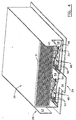
- FIG. 4 there are shown respectively a perspective view of a power converter module which provides a belt-like current path in accordance with the present invention, and the same module with cut parts to expose an interior portion thereof.
- the low stray interconnection inductance power converting module is for converting a DC voltage into an AC voltage. It comprises two DC voltage terminals 20 and 22 for receiving the DC voltage, and an AC voltage terminal 24 for delivering the AC voltage. There is also provided a half-bridge including a pair of power switching elements 26 and 28 connected as a series totem pole between the DC voltage terminals 20 and 22 via the AC voltage terminal 24. There is a decoupling device 30 for decoupling the half-bridge.
- the decoupling device 30 comprises a series of at least two adjacent superimposed electrode plates 31 separated by a dielectric material and extending proximately in overlapping relation with the half bridge. Each of the adjacent electrode plates 31 is connected to a different one of the DC terminals 20 and 22.
- the electrode plates 31 form with the two power switching elements 26 and 28, the DC terminals 20 and 22, and the AC terminal 24 a reduced cross section belt-like current closed loop 64 by which a low stray interconnection power converting module is obtained.
- the superimposed electrode plates 31 form a capacitance.
- the power converting module comprises a base 32 made of ceramic material, onto which the power switching elements 26 and 28 are mounted.
- Each of the power switching elements 26 and 28 includes a row of power semiconductor devices mounted in parallel.
- the AC terminal 24 includes a central metal plate 34 mounted on the base 32.
- Each of the two DC voltage terminals 20 and 22 includes a lateral metal plate 36 or 38 mounted onto the base 32, and a lateral upright metal wall 40 or 42 connected between the corresponding lateral metal plate 36 or 38 and the decoupling device 30.
- the power switching elements 26 and 28 are connected as a series totem pole between the lateral metal plates 36 and 38 of the DC voltage terminals 20 and 22 via the central metal plate 34 of the AC voltage terminal 24.
- each row of power semiconductor devices comprises MOSFETs, IGBTs and/or diodes.
- the module further comprises drivers 54 mounted on the base 32 nearby the MOSFETs or IGBTs, to bring the gate signal to the MOSFETs or IGBTs.
- a driver is defined as a board provided with electronic components for supplying through output connecting pads an analog gate signal to the gate of the semiconductor chips.
- the reduced cross section belt-like current closed loop is defined by the central plate 34, the lateral metal plates 36 and 38, the lateral upright metal walls 40 and 42, the superimposed electrode plates 31 and the switching elements 26 and 28. This belt-like current closed loop has a rectangular cross section.
- the method for converting a DC voltage into an AC voltage comprises the step of applying the DC voltage on two DC voltage terminals 20 and 22 between which a half-bridge is connected, the half-bridge including a pair of power switching elements 26 and 28 connected as a series totem pole between the DC voltage terminals 20 and 22 via an AC voltage terminal 24.
- a decoupling device 30 comprising a series of at least two adjacent superimposed electrode plates 31 separated by a dielectric material and extending proximately in overlapping relation with the half bridge, each of the adjacent electrode plates 31 being connected to a different one of the DC terminals 20 and 22.
- the electrode plates 31 form with the two power switching elements 26 and 28, the DC terminals 20 and 22, and the AC terminal 24 a reduced cross section belt-like current closed loop.
- delivering the AC voltage by means of the AC voltage terminal 24.
- the plates 36, 38 and 34 are conductive strips provided on the base 32 which is made of an insulating substrate, such as an alumina or aluminum-nitride. The strips are placed in parallel and along direction A.
- a first row of semiconductor chips 46 and a second row of semiconductor chips 48, such as Mosfets, IGBTs and/or diodes, are mounted respectively on the surface of the conductive plates 36 and 34.
- the semiconductors chips 46 and 48 are electrically linked with their respective conductive plates 36 and 34.
- the surface connecting pads of the first rows of semiconductor chips 46 are electrically linked with bounding wires 50 to the conductive plate 34.
- the connecting pads of the second rows of semiconductor chips 48 are electrically linked with bounding wires 52 to the conductive plate 38.
- driver boards 54 made with insulating substrate, such as alumina are placed in proximity of the chips to provide gate signals trough the bounding wires 56.
- the whole assembly constitutes a half bridge power converter circuit.
- the assembly of the plates 31 forms a capacitor.
- This capacitor is directly connected in parallel to the half bridge power converter mounted thereunder.
- the terminal 22 is for receiving the first electrode of a bipolar DC voltage source (not shown).
- the terminal 20 is for receiving the second electrode of the bipolar DC voltage source.
- the terminal 24 is for connection with a load (not shown). Thereby, the whole assembly supplies AC voltage to the load via the operation of the half bridge power converter.
- the locations of the connecting points on the terminals 20, 22 and 24 are not critical in the power converter and can be made where it would be most convenient for electrical, mechanical or assembly purposes.
- the module of the present invention comprises several parallelled half bridge converters each made of two semiconductor chips 46 and 48 mounted in a totem configuration.
- Each of the semiconductor chips 46 and 48 is made of a diode chip connected in parallel to a IGBT chip. These half bridge converters are disposed in parallel along direction A to increase current capability.
- the capacitor 30 is connected directly across all parallelled half bridge converters. Thus, direct decoupling of all of the half bridge converters is obtained, and possible oscillations between adjacent half bridge converters during turn-on or turn-off phase because of stray interconnection inductances are avoided. Furthermore, the positions and the boundings of the chips 46, 48 are done to obtain a uniform distribution of the current along direction A. Thus, the transient current loop path are oriented along direction B.
- the capacitor made by the plates 31 acts as a short-circuit for transient currents, so that the current change occurring during a switching sequence of the power converter follows a belt-like path 64 similar to the tubular geometry shown in figure 3.
- this assembly has a stray interconnection inductance substantially equivalent to the inductance of a cylinder coil having the same cross section area and length.
- This stray interconnection inductance is very low thereby reducing the voltage spike generated across the switching elements 26, 28, allowing higher switching speed, avoiding the use of clamping devices or snubbers, allowing a control of the current falling rate by means of the switch, allowing several switching devices to be parallelled, reducing the losses due to the stray interconnection inductance L 2 itself, and reducing the size of the converter.
- FIG 6 there is shown a cut view in perspective of another embodiment of the present invention.
- two terminals 24 and 25 including respectively plates 34 and 35 are mounted side by side on the insulating substrate 32 along direction A.
- a first half 60 of the row of semiconductor chips 48 is mounted on the plate 34.
- a second half 62 of the row of semiconductor chips 49 is mounted on the plate 35.
- the bounding wires 50 of the first half 60 of the row of semiconductor chips 46 mounted on plate 36 are electrically connected to the plate 34 and the bounding wires 51 of the second half 62 of the row of semiconductor chips 47 mounted on plate 36 are electrically connected to the plate 35.
- two groups of driver boards 54 and 55 are placed respectively in proximity to their group of chips 48, 49 to provide gate signals trough the bounding wires 56. Thereby this whole assembly now has two half bridge power converters.
- the terminals 24 and 25 are for connection with the two end terminals of one load (not shown) or the first end terminal of two loads (not shown) with their other end terminal connected to one of the voltage source electrode.
- two AC voltages are supplied to the loads by means of two half bridge power converters.
- these two half bridge power converters produce transient current belt-like paths 64 and 66 similar to what is shown in figure 3.
- the stray interconnection inductance L 2 for each half bridge is equivalent to the inductance of a cylinder coil having the same cross section area and length, this stray interconnection inductance being very low, hence reducing the voltage spike generated across the switches, allowing higher switching frequency and reducing the losses relating to the stray interconnection inductance itself.
- the locations of the connecting points on the terminals 24 and 25 are not critical in the power converter and can be made where it would be most convenient for electrical, mechanical or assembly purposes.
- the present embodiment can be easily adapted for more than two half bridge power converters.
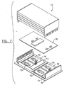
- FIG. 7 is a disassembled view of the module
- figure 8 is an assembled view of the same module.
- Four large power Mosfet chips 70 with built in free wheel diodes are used as semiconductor chips. These chips 70 are characterized by ultra fast turn off speed capability.
- the insulating substrate 32 is made of alumina.
- a multi layer ceramic capacitor 72 is mounted on top of the assembly. Thereby the whole assembly forms one half bridge power converter similar to the one shown in figure 4.
- Two gate drivers 74 are mounted on conductive plates 76, in close proximity to the power Mosfets chips 70.
- a control board 78, operating with the drivers 74 is inserted in a gap located underneath the capacitor 72 when the module is assembled.
- the control board 78 comprises digital and analog components such as a micro-controller with sensors and amplifiers ; digital inputs/outputs to be linked with a master controller ; and analog outputs to drive the semiconductor chips via the drivers 74.
- a number of conductive links electrically connect the control board 78 to the drivers 74 so that gate control signals are provided to the power Mosfets 70 via the driver 74 and the control board 78.
- the control board 78 supports the analog and the logic circuit not required on the ceramic base, thus reducing significantly the size of the substrate 32.
- the increase of the gap to insert the control board 78 has less impact on the stray interconnection inductance compared to the impact resulting from an increase of the substrate surface along direction B.
- This control board 78 is not shown in the previous figures to not overload them.
- the numbers 80 and 82 indicate cross section surfaces that will be referred to later in the description.
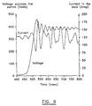
- FIG 9 there is shown the voltage measured directly across one row of the Mosfet chips 70 shown in figures 7 and 8 during a turn off sequence of the current flowing through the Mosfet chips 70.
- the cutoff current is at 125 amperes and is coming from an inductive load while the operating bus voltage is at 400 volts. It can be observed that the voltage has a spike with a ringing decay caused by the oscillation of a stray interconnection inductance L 2 that is in series with the output capacitance of the Mosfet chips supporting the voltage. The energy contained within the oscillation is eliminated by joule effect in the resistive links.
- the stray interconnection inductance L 2 can be evaluated by means of the damping frequency and a 2 nd order equation of the series resonant LCR circuit.
- the damped frequency of the voltage shown in figure 9 is about 40 Mhz, and the voltage oscillates around 400 volts.
- the magnetic flux responsible for the induced voltage spike passes in part through the cross section 80 between the substrate 32 and the capacitor 72.
- the other part of the flux passes through the cross section 82 in the capacitor 72 and depends solely on the current change distribution within the multi layer geometry of the capacitor.
- the skin depth in the capacitor electrodes has a value comparable to the thickness of one of its electrode plates so that the total current gradient loop flows in the first lower layers of the superimposed conductive electrode plates.
- no magnetic flux appears in the upper part of the capacitor, the magnetic flux passing mostly in the cross section 80.
- any flux change within the capacitor 30 is cancelled by internal current loop therefore no high frequency flux change can exist within the body of capacitor 30.
- the cross section 80 of the prototype that has been confidentially tested is about 5.5 x 10 -4 m 2 and the length of the module is about 0.03 metres.
- a cylindrical current loop with an equivalent cross section has a diameter equal to 0.026 metres.
- the inductance computed with equation (1) is equal to 16.6 x 10 -9 Henry.
- the lower interconnection inductance L 2 deduced from the equation (4) can be attributed to the presence of capacitor 30 and to the presence of the large aluminum heat sink to which the module was clamped.
- the heat sink as its conductive surface reacts with the magnetic field distribution produced by current gradient loop during the switching sequence, the flux change in the inductance is reduced. Consequently, an equivalent stray interconnection inductance that is lower than what is expected is obtained.
- voltage spike can be decreased by lowering the stray inductance L 2 . This is achieved by reducing the cross section 80. Unfortunately, some space has to be allowed for inserting the control board 78 and to clear the bounding wires 50, 52. But a further reduction of the voltage spike can be achieved by using a second conductive closed loop that reduces the flux changes in the stray interconnection inductance. This second conductive closed loop will be referred to as a spike killer.
- the module has conductive walls 21 placed respectively at both ends of the module. These walls 21 cover at least the cross section 80 of the module shown in figure 8. Each of these conductive walls 21 could be connected to one of the three terminals 20, 22 and 24.
- the cylindrical current path and the walls at both ends are like two coils with a mutual coupling that is not perfectly matched due to their relative position compared to each other so that only a portion of the flux source fluctuation is reduced.
- the magnetic field H 1 generated by the cylindrical current loop 110 is surrounded by a second cylindrical conductive loop 112.
- the second loop 112 matches as closely as possible the path followed by the first current loop 110.
- any magnetic field H 1 generated by a current I 1 produces a magnetic flux density that is also embraced by the second cylindrical loop 112.
- Any change of the cylindrical current I 1 produces a voltage drop within the cylindrical conductive loop path 112 due to the flux variation.
- a cylindrical current change I 2 in opposite direction, immediately appears in reaction with the presence of the voltage drop, to produce a magnetic field H 2 in opposition to the magnetic field source H 1 .
- This magnetic field H 2 reduces the resulting magnetic flux change.
- FIG 13 there is shown an electric circuit equivalent to the two concentric cylindrical loops 110, 112 of figure 12.
- the loops 110, 112 are represented by a transformer that has its secondary winding (not shown) shorted.
- a current source I 1 connected in series to a circuit composed of a mutual inductance M representative of the flux embraced by the two cylinders 110, 112 plus two very small leakage inductances L 3 and L 4 associated to the leakage flux, generated by one of the two cylinders 110, 112 and not embraced by the other, due to improper matching.
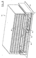
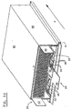
- FIG 14 there is shown a perspective view of a module with a second conductive closed loop in accordance with the present invention.
- the module assembly is similar to the one shown in figure 4 except that it further comprises a housing including conductive walls 90 surrounding the reduced cross section belt-like current closed loop 64 shown in figure 5, whereby, in operation, an electric current is magnetically induced into the conductive walls 90 to further reduce voltage spikes associated to stray interconnection inductance.
- the conductive walls 90 surrounds the module assembly along direction A. These conductive walls 90 are insulated from the conductive parts within the module assembly by an insulating material 91. These conductive walls 90 form a closed loop which embraces the magnetic flux density generated by the transient belt-like current of the half bridge power converter during the switching sequence.
- the method for converting a DC voltage into an AC voltage comprises the additional step of surrounding the reduced cross section belt-like current closed loop by means of a housing including conductive walls.
- the spike killer described above acts like a clamping device which maintains constant most of the magnetic field produced in the belt-like current closed loop 64 shown in figure 5 during the switching operation.
- the energy contained in the magnetic field is stored in the mutual stray inductance M that has a value near to the stray inductance L 2 shown in figure 1.
- FIG 15 there is shown a circuit diagram representative of a power converter including the module shown in figure 14, assuming that there is a sufficient good matching between the two closed loops to neglect leakage inductances L 3 and L 4 shown in figure 13.
- the current distribution can be represented by four mesh currents I 1 , I 2 , I Load , and I Source .
- the mesh currents I Load and I Source are continuous and thus do not produce significant current discontinuity.
- a high flux change is generated by changes in mesh currents I 1 and I 2 . This high flux is dependent upon the geometry of path of currents I 1 and I 2 .
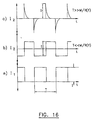
- FIGS 16(a), (b) and (c) there are shown curves illustrating the AC mesh currents I 1 and I 2 of figure 15 with respect to time.
- Mesh current I 2 is shown for two different switching periods T such as T ⁇ M/R(f) and T>>M/R(f).
- the spike killer reacts to any flux change by producing a current that suppresses this flux change during the switching phase.
- the life time of the flux produced by the spike killer depends on its time constant M/R(f), the time period between the switching sequences being T.
- the magnetic energy stored by the spike killer vanishes in joule losses within its conductive loop as shown in figure 16(c) combined with figure 16(a).
- the total amount of losses in watts equals the product of the amount of magnetic energy loss between each switching event by the switching frequency of the switching events.
- the spike killer acts as a dissipative clamping device.
- the major portion of the magnetic energy stored in the spike killer is still present at the beginning of the next switching phase as shown in figures 16(a) and (b).
- the losses relative to the magnetic energy in Joule in the spike killer do not increase anymore linearly with the switching frequency because the magnetic energy is rather exchange between the mesh currents I 1 and I 2 .
- the spike killer acts as an inductance reducer that further lowers the mutual stray inductance M of the power converter module.
- the spike killer of the present invention limits its power losses as the switching frequency increases. Also, the spike killer acts directly on the stray interconnection inductance to maintain the presence of the stored magnetic energy during the switching phases. Therefore, no energy is pumped out from the DC supply source because of this inductance as it is in cases where a traditional clamping device is used, and the current falling rate is still under the control of the switch.
- the spike killer can be carried out according to the present invention by closing both ends of the first or second belt-like current closed loop with conductive walls.
- this has no meaningful spike killing effect.
- a more efficient spike killing effect is achieved by having two concentric belt-like current closed loops that are as close as possible with each other without being in contact to minimize the leakage flux generated by the first belt like current loop and not embraced by the second belt like conductive loop.
- a thin insulating material 91 gives good results.
- Both open ends can serve as passage for the electrical and logical cable links.
- the conductive walls of the spike killer could be part of the module housing which can serve as a heat exchanger.
- a spike killer With the use of a spike killer according to the present invention, flux fluctuations within the mutual inductance M are reduced to minimum to further reduce the voltage spikes, allow a much higher switching speed, avoid the use of clamping devices or snubbers, allow a control of the current falling rate by the semiconductor switches, allow several switching devices to be mounted in parallel, limit losses related to the mutual stray interconnection inductance for high switching frequency, and reduce the size of the converter.
- the power converting module is therefore provided with a spike killer, according to the present invention.
- the housing includes the conductive walls 90 surrounding the reduced cross section belt-like current closed loop, whereby, in operation, an electric current is magnetically induced into the conductive walls 90 to reduce the flux change within the mutual stray interconnection inductance.
- the method of converting a DC voltage into an AC voltage comprises in this case the additional step of surrounding the reduced cross section belt-like current closed loop by means of a housing including conductive walls 90.
- the module assembly shown in figure 14 is similar to the one shown in figure 4 but it further comprises the conductive walls 90 extending along direction A. These conductive walls 90 are insulated from the conductive parts within the module assembly by the insulating material 91. These conductive walls 90 form a closed loop which embraces the magnetic field generated by the transient belt-like current of the half bridge power converter during the switching sequence. Hence, the conductive walls 90 reacts and induces an opposite magnetic field which reduces the amplitude of the magnetic flux change generated in the module, thereby reducing the voltage spike generated by the mutual stray interconnection inductance M. With this assembly, a resulting mutual stray interconnection inductance M that is lower than the one of prior art, or equal to the one of embodiment of figures 4, 5 and 6 is obtained.
- This lower mutual stray interconnection inductance reduces the voltage spike, allows a much higher switching speed, avoids the use of clamping devices or snubbers, allows a control of the current falling rate by the semiconductor switches, allows several switching devices to be mounted in parallel, limits losses related to the mutual stray interconnection inductance for high switching frequency, and reduces the size of the converter.
- FIG. 17 is a disassembled view of the module with the spike killer
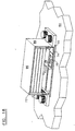
- figure 18 is an assembled view of the same module.
- the module base 32 is mounted on a copper plate 94 and a cover 96 is bolted on the copper plate 94.
- This cover 96 and the copper plate 94 form a second belt-like conductive path around the first belt-like conductive path in a concentric fashion as shown in figure 12.
- the conductive walls of the housing are then made of at least two parts connected together, which are the cover 96 and the copper plate 94.
- Connectors for receiving voltage from the bus DC voltage source and for supplying the modulated phase are located in the open ends of the module. Small openings can be performed on the conductive walls of the belt-like conductive paths for electrical connections with terminals within the module without affecting noticeably the reducing effect on the flux change in the mutual stray interconnection inductance.
- FIG 19 there is shown the voltage measured directly across one row of the Mosfet chips 70 of the embodiment shown in figures 17 and 18 during a turn-off sequence of the current flowing through the Mosfet chips 70.
- the cutoff current is also 125 amperes and is coming from the same inductive load with the bus voltage also at 400 volts.
- the voltage oscillation seen in figure 9 is practically gone and the voltage spike is reduced, therefore showing the advantage of the addition of the second belt-like conductive path.
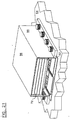
- FIG. 20 is a disassembled view of the module
- figure 21 is an assembled view of the same module.
- the assembly has a length that is three times longer along the direction A than the length of the embodiment shown in figures 17 and 18.
- the insulating gap between the second belt-like conductive path and the first belt-like conductive path, and the gap between the base plate and the decoupling means are reduced with respect to the embodiment shown in figures 17 and 18.
- Eight IGBT chips with eight diode chips are connected in parallel for each row of the module. With this assembly, the mutual stray interconnection inductance is smaller due to the larger l/d ratio of the module as shown in equation (1), 1 and d of the module being defined as shown in figure 3.
- FIG 22 there is shown the result of switching tests performed on the module shown in figures 20 and 21.
- the voltage is measured across one row of IGBT chips 100 during a switching test.
- the cutoff current is 45 amps and the bus voltage is set at 500 volts.
- the test shows a turn off sequence with no apparent voltage spike and the voltage swings from 0 to 500 volts in less than 20 nsec.
- the improvement is due to the larger l/d ratio, the smaller insulating gap between the two belt-like conductive paths, and the smaller gap between the base plate and the decoupling means which further reduce the voltage spike generated in the stray interconnection inductance as compared to the embodiment of figures 17 and 18, thereby illustrating the efficiency of the present invention.
- the spike killer of the present invention can be made according to different embodiments.
- the modules shown in figures 17, 18, 20 and 21 illustrate a belt-like conductive loop having two parts.
- the first part is the cover 96 which is made of conductive material, such as copper or aluminum.
- This cover 96 has two sides welded or clamped with securing elements, such as bolts, to the conductive base plate 94 placed underneath the module insulating base 32.
- the plate 94 constitutes the second part of the loop.
- the base plate 94 can form a heat exchanger or can be bounded underneath of the insulating plate 32, such as a copper bound layout bounded underneath a copper-ceramic-copper board.
- the spike killer is separated from the module with insulating material, (not shown).
- a spike killer can be also made by using a thin film metal deposition.
- the conductive walls 90 of the housing shown in figure 14 are then formed by a metal deposition over insulating walls 91.
- the module is first encapsulated in a plastic or any other material with insulating properties and is then sprayed with a metallic vapor or dipped in a liquid metal bath to form a thin film metal deposit on its surface.
- This metal deposit forms the belt-like conductive loop of the spike killer.
- the thin film deposit may be only applied on specified portions of the module such as for example, the top and the sides thereof, the remaining part of the belt-like conductive loop being a copper layout bounded underneath the surface of the insulating base 32.
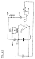
- FIG 23 there is a schematic circuit diagram representing a power converter including the module shown in figure 14.
- a problem often occurs because of the stray capacitance present between the load and an adjacent conductive part such as, for example, the stray capacitance present between the stator coils of a motor and its metal hollow portion. This problem is schematized in the diagram of figure 23.
- a half bridge power converter 121 supplies AC voltage to a load 120 having a stray capacitance 122 with a conductive part 124.
- the potential of the conductive part 124 oscillates at a frequency in accordance with the square wave voltage applied to the load 120 by the half bridge power converter 121.
- Any form of stray impedance connected between the load housing and one of the electrodes 126, 128 of the DC supply voltage bus produces a current through the stray capacitance 122. This current is a source of noise problems and may be harmful.
- a bypass capacitor 130 with a higher value than the one of the stray capacitor 122 is connected between the conductive part 124 and at least one of the bus voltage electrodes, for instance the electrode 128.
- the induced stray current within the stray capacitance 122 follows an easy path through the capacitor 130 back to the bus electrode 128.
- the amplitude of the voltage that builds up on the bypass capacitor 130 is a fraction of the supply voltage, the value of this fraction being determined by the ratio of the stray capacitor value with respect to the bypass capacitor value.
- this bypass capacitor can have one end connected to one of the electrode terminals 20 or 22 of the module.
- the free end of the capacitor is available for connection with a conductive part producing a stray capacitance with the load (not shown).
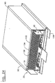
- FIG 24 there is shown an embodiment similar with the one shown in figure 14, but it further includes a built-in bypass capacitor.
- the free end of the capacitor is connected to the walls 90 of the belt-like conductive loop of the spike killer, and a free connection point 138 of the spike killer is available on the conductive loop for connection to a conductive part (not shown) that forms a stray capacitance with the load. If this capacitor is a discrete part, it can be inserted in a space located between the conductive walls 90 of the spike killer and the module.
- a horizontal conductive plate 134 is superimposed over the top last conductive plate 132 of the superimposed electrode plates 31, and separated therefrom by a dielectric material 136, such as ceramic, the whole thereby forming said built-in bypass capacitor.
- the conductive plate 134 constitutes one segment of the belt-like conductive walls 90 of the spike killer.
- the gap shown in this figure between the plate 134 and the last plate 132 is larger than the existing gap which is actually the same as the one between adjacent plates of the superimposed electrode plates 31.
- the connection point 138 can be located anywhere on the conductive walls 90 of the spike killer for connection with the conductive part 124.
- the capacitor is connected between the conductive plate 134 which is part of the conductive walls 90 of the housing, and the conductive plate 132 which is electrically connected to one of the DC terminals.
- the conductive walls provide one connecting point 138 for electrical connection purpose.
- the capacitor is then formed by a wall of the conductive walls that is adjacent to the top electrode plate 132 and that is separated from the top electrode plate 132 by means of dielectric material 136.
- the fact that the module has a very low stray interconnection inductance which is further clamped by the spike killer does not produce a Miller effect (reference: International Rectifier, Hexfet, Power MOSFET designer's Manual, application note #947) during the switching phase.
- This Miller effect is present in gate capacitance transistors such as Mosfets and IGBTs.
- the drain current is controlled by the amount of charges cumulated in its gate to source capacitance. During the turn-on phase, the drain voltage falls because the increasing drain current induces a voltage across the interconnection inductance.
- the voltage drop at the interconnection inductance is negligible so that the Miller effect is not present.
- the input gate current is not bypassed and serves only to charge the gate to source capacitance of the Mosfet or IGBT. Therefore, the drain current rising rate depends only on the input gate charging current.
- the rising time of the drain or collector current is very short. This can result in a problem if the switch that is turned on takes over the current of an inductive load that flows, in a free wheel mode, through a diode having a reverse recovery charge.
- a high current rising rate increases the reverse recovery current density within the diode and the Mosfet or IGBT, which can be destructive for the semiconductors.
- the gate input charging current is limited with a resistor to limit the rising current rate.
- the drain voltage falling rate is dependent on the same input gate current now discharging the gate to drain capacitance. This drain voltage falling rate is less problematic and can be accelerated to minimize switching losses. This is carried out by injecting a higher gate input current to improve the switching performance.
- FIG 25 there is shown a circuit diagram of a switch with its driver.
- the gate input current is limited to two values, one for the rising current and one for the falling voltage. This function is performed by means of the driver.
- the driver includes a terminal 220 to receive a gate signal for the corresponding semiconductor device.
- a first resistor R 1 is connected between the terminal 220 and the gate 222 of the corresponding semiconductor device 224.
- circuit segment including a voltage gate controlled switch T 1 and a second resistor R 2 connected in series. The circuit is connected in parallel to the first resistor R 1 .
- a capacitor C 1 is connected between the gate 226 of the voltage gate controlled switch T 1 and the collector 228 of the corresponding semiconductor device 224 for monitoring collector voltage signal thereof.
- the first resistor R 1 limits gate current of the corresponding semiconductor device prior to a drop of the collector voltage signal thereby limiting rise time of the collector current
- the first and second resistors R 1 and R 2 limit the gate current of the corresponding semiconductor device 224 during the drop of the collector voltage thereby limiting dropping time of collector voltage.
- a first resistor R 1 is connected between the input that receives the square voltage signal and the gate 222 of the switch 224 to limit the gate input charging current to a first value Ig 1 , until the current flowing through the diode D evacuates its reverse recovery charges and enters its blocking state. Then, the drain voltage starts to fall and is detected by a capacitor C 1 connected between the drain 228 of the switch 224 and the gate 226 of a P channel Mosfet T 1 that is connected in series with a second resistor R 2 .
- the switch 224 is a Mosfet
- the capacitor C 1 is connected to the drain 228, and when the switch 224 is an IGBT, the capacitor is connected to the collector.
- the Mosfet T 1 and resistor R 2 are both in parallel to resistor R 1 .
- the dropping voltage induces a current through the capacitor C 1 which charges rapidly the gate of the P channel Mosfet T 1 which immediately conducts to establish a series connection with the resistor R 2 .
- the input current is increased by a second gate input charging current Ig 2 , further accentuating the voltage dropping rate to increase the switching speed, thereby reducing the switching losses.
- a clamping means X 1 is connected across the gate capacitance of the P channel Mosfet T 1 to limit the voltage.
- a capacitor C 2 connected in series with a resistor R 3 is added in parallel with the resistor R 1 , to inject a current pulse in the gate 222 to shorten the delay between the input voltage transition and the start of the drain current rise-up.
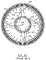
- FIG 26 there is shown one of the possible applications of the present invention.
- the electric motor is mounted in a wheel, the power converter of the motor being mounted in a hollow portion of the wheel.
- the motor has an outer rotor 200 and an inner stator 201 supported on an axle by a cross member 204.
- the power converter includes modules 205 and capacitors 206, all mounted on the legs of the supporting cross member 204.
- Conductors 207 are provided to connect each module to a DC voltage bus provided in the hollow portion, and to connect each module to the windings of the stator.
- the modules constitute a polyphase DC to AC power converter. The compactness of the modules of the present invention makes them convenient for installation within the hollow portion of the motor wheel.
- FIG 27 there is shown how the power converter of the present invention is mounted on the cross member 204 of the motor wheel.
- the three power converting modules 205 in a motor wheel provided with a stator frame supported by a cross member 204 made of conductive material.
- the three modules 205 are mounted respectively on three legs of the cross member 204 within the motor wheel.
- the modules 205 form a three-phase power converter which further comprises a first conductive bus having a pole 209 connected to one of the DC terminals of each module 205 with a feed-trough connector 211 on one side of the cross member 204.
- a second conductive bus having a pole (not shown but similar to pole 209 with connectors similar to connectors 211) connected the other of the DC terminals of each module on the other side of the cross member 204.
- the two conductive bus delimit spaces between adjacent modules that are filled with the conductive material of the cross member 204.
- the two conductive bus are separated from the module housing and the cross member 204 by insulating material 210, whereby, in operation, an electric current is magnetically induced in the cross member 204 to suppress the magnetic flux change generated in the stray interconnection inductance present between the modules.
- the machine is a three-phase permanent magnet AC machine.
- Three modules 205 each containing one half bridge power converter, one for each phase, are mounted on the legs of the cross member 204. There is one module per leg. Each leg acts as a heat exchanger for the corresponding module.
- the bipolar DC voltage bus provided in the hollow portion has one pole 209 connected with feed-trough connectors 211 to terminal 22 of a module such as the one shown for example in figure 4. All the connections are located on one side of the cross member 204.
- the other pole (not shown but similar to pole 209 with connectors similar to the connectors 211) of the DC voltage bus is connected to the other terminal 20 of the module of figure 4, all the connections being located on the other side of the cross member 204.
- Each pole is isolated from the conductive part of the cross member and the module housing with an insulating layer 210.
- the stray inductive interconnection linking the modules 205 may cause a voltage oscillation between each module capacitor due to the fact that the load current are switched by each module and that this switching alternates from one pole to the other.
- the interconnection inductance has to be minimized.
- One known method for minimizing interconnection inductance is to connect two adjacent modules by means of two conductive strips mounted side by side and separated with a thin insulating material. To minimize interconnection inductance with the present invention, it requires that one interconnection passes from one side of the module to the other side.
- a simpler connection is made by directly linking the modules by means of straight interconnections located alongside legs of the cross member, as shown in figure 27.
- the volume between two adjacent interconnections and between two adjacent modules is completely filled with the conductive material, such as aluminum, of the cross member 204.
- the conductive material such as aluminum
- the interconnection inductance of a power converter assembly is greatly reduced by integrating the power electronics switching devices, the DC terminals, the AC terminal and a capacitor within one package characterized with a belt-like current closed loop.
- the voltage spike induced in the interconnection inductance can be further reduced by adding a second belt-like closed loop, referred here as a spike killer, which surrounds the module to embrace in the belt-like transient current loop circulation generated in the module during a switching event.
- the reduced interconnection inductance and the spike killer allows a higher switching speed and frequency with a lower voltage spike across the switches thus improving the efficiency of the power converter.
Landscapes
- Engineering & Computer Science (AREA)
- Power Engineering (AREA)
- Inverter Devices (AREA)
- Rectifiers (AREA)
- Power Conversion In General (AREA)
Claims (15)
- Leistungsumsetzungsmodul mit niedriger Verbindungsinduktivitätsstreuung, das eine Gleichspannung in eine Wechselspannung umsetzt und versehen ist mit zwei Gleichspannungsanschlüssen zum Empfangen der Gleichspannung; einem Wechselspannungsanschluß zum Liefern der Wechselspannung; einer Halbbrücke, die ein Paar Leistungsschaltelemente enthält, die als eine Totempfahl-Reihenschaltung über den Wechselspannungsanschluß zwischen die Gleichspannungsanschlüsse geschaltet sind; und einem Entkopplungsmittel zum Entkoppeln der Halbbrücke, wobei das Entkopplungsmittel eine Reihenschaltung aus wenigstens zwei benachbarten übereinanderliegenden Elektrodenplatten, die durch ein dielektrisches Material getrennt sind, umfaßt, wobei jede der benachbarten Elektrodenplatten mit einem anderen der Gleichspannungsanschlüsse verbunden ist, wobei das Leistungsumsetzungsmodul mit geringer Verbindungsinduktivitätsstreuung dadurch gekennzeichnet ist, daß:die wenigstens zwei benachbarten übereinanderliegenden Elektrodenplatten sich in geringem Abstand und in überlappender Beziehung zu der Halbbrücke erstrecken; unddie Elektrodenplatten mit den beiden Leistungsschaltelementen, den Gleichspannungsanschlüssen und dem Wechselspannungsanschluß einen riemenählichen Leitungspfad mit verringertem Querschnitt in Form einer geschlossenen Schleife bilden.
- Leistungsumsetzungsmodul nach Anspruch 1, das eine aus einem keramischen Werkstoff hergestellte Grundplatte enthält, auf der die Leistungsschaltelemente montiert sind, und bei dem:jedes der Leistungsschaltelemente eine Reihe aus zueinander parallelgeschalteten Leistungshalbleitervorrichtungen enthält;der Wechselspannungsanschluß eine auf der Grundplatte montierte mittige Metallplatte enthält; undjeder der beiden Gleichspannungsanschlüsse eine auf der Grundplatte montierte seitliche Metallplatte und eine seitliche, aufrechtstehende Metallwand, die zwischen der seitlichen Metallplatte und den Entkopplungsmitteln angeschlossen ist, enthält, wobei die Leistungsschaltelemente als eine Totempfahl-Reihenschaltung über die mittige Metallplatte des Wechselspannungsanschlusses zwischen die seitlichen Metallplatten der Gleichspannungsanschlüsse geschaltet sind.
- Leistungsumsetzungsmodul nach Anspruch 2, bei dem der riemenähnliche leitende Pfad mit verringertem Querschnitt in Form einer geschlossenen Schleife durch die mittige Platte, die seitlichen Metallplatten, die seitlichen, aufrechtstehenden Metallwände, die übereinanderliegenden Elektrodenplatten und die Leistungsschaltelemente gebildet ist und einen rechtwinkligen Querschnitt aufweist.
- Leistungsumsetzungsmodul nach Anspruch 2 oder 3, das ferner Treiber umfaßt, die auf der Grundplatte in der Nähe der Leistungshalbleitervorrichtungen montiert sind, die die Leistungshalbleitervorrichtungen anzusteuern.
- Leistungsumsetzungsmodul nach Anspruch 4, bei dem die Halbleitervorrichtungen über die Gate-Kapazität gesteuerte Halbleitervorrichtungen sind und jeder der Treiber enthält:einen Anschluß, der ein Gate-Signal für die entsprechende Halbleitervorrichtung empfängt;einen ersten Widerstand, der zwischen den Anschluß und ein Gate der entsprechenden Halbleitervorrichtung geschaltet ist;ein Schaltungssegment, das einen durch die Gatespannung gesteuerten Schalter und einen zweiten Widerstand, die in Reihe geschaltet sind, enthält, wobei die Schaltung zum ersten Widerstand parallelgeschaltet ist;einen Kondensator, der zwischen ein Gate des durch die Gatespannung gesteuerten Schalters und den Kollektor der entsprechenden Halbleitervorrichtung geschaltet ist, um ein Kollektorspannungssignal der entsprechenden Halbleitervorrichtung zu überwachen;ein Spannungsklemmittel, das zwischen das Gate des durch die Gatespannung gesteuerten Schalters und den Anschluß geschaltet ist, wobei im Betrieb der erste Widerstand den Gatestrom der entsprechenden Halbleitervorrichtung vor einem Abfall des Kollektorspannungssignals begrenzt, wodurch die Anstiegszeit des Kollektorstroms begrenzt wird, und wobei im Betrieb die ersten und zweiten Widerstände den Gatestrom der entsprechenden Halbleitervorrichtung während des Abfalls der Kollektorspannung begrenzen, wodurch die Abfallzeit der Kollektorspannung begrenzt wird.
- Leistungsumsetzungsmodul nach Anspruch 2, 3, 4 oder 5, das ein Steuerboard zum Steuern der Leistungshalbleitervorrichtungen umfaßt, das sich zwischen der Grundplatte, auf der die Leistungsschaltelemente montiert sind, und den Entkopplungsmitteln befindet.
- Leistungsumsetzungsmodul nach Anspruch 1, 2, 3, 4, 5 oder 6, das ferner Wände umfaßt, die aus einem leitenden Werkstoff hergestellt sind, um offene Enden des riemenähnlichen Leitungspfades in Form einer geschlossenen Schleife zu verschließen, wobei jedes der offenen Enden durch die Kanten der mittigen Platte, der seitlichen Platten und der seitlichen Metallwände sowie durch eine untere Kante der übereinanderliegenden Metallplatten begrenzt ist, wobei im Betrieb in die leitenden Wände ein elektrischer Strom magnetisch induziert wird, um Spannungsspitzen, die mit der Verbindungsinduktivitätsstreuung einhergehen, weiter zu verringern.
- Leistungsumsetzungsmodul nach Anspruch 1, 2, 3, 4, 5 oder 6, das ferner ein Gehäuse umfaßt, das die leitenden Wände enthält, die den riemenähnlichen Leitungspfad mit verringertem Querschnitt in Form einer geschlossenen Schleife umgeben, wobei im Betrieb in die leitenden Wände ein elektrischer Strom magnetisch induziert wird, um Spannungsspitzen, die mit der Verbindungsinduktivitätsstreuung einhergehen, weiter zu verringern.
- Leistungsumsetzungsmodul nach Anspruch 8, bei dem wenigstens eine der leitenden Wände des Gehäuses durch eine Metallablagerung auf isolierenden Wänden gebildet ist.
- Leistungsumsetzungsmodul nach Anspruch 8 oder 9, bei dem die leitenden Wände des Gehäuses aus wenigstens zwei miteinander verbundenen Teilen hergestellt sind.
- Leistungsumsetzungsmodul nach Anspruch 8, 9 oder 10, das ferner einen Kondensator umfaßt, der zwischen die leitenden Wände des Gehäuses und einen der Gleichspannungsanschlüsse geschaltet ist, wobei die leitenden Wände einen Verbindungspunkt für eine elektrische Verbindung schaffen.
- Leistungsumsetzungsmodul nach Anspruch 11, bei dem der Kondensator durch eine Wand der leitenden Wände gebildet ist, die an eine obere Elektrodenplatte der Entkopplungsmittel angrenzt und von der oberen Elektrodenplatte durch ein dielektrisches Material getrennt ist.
- Kombination aus drei Leistungsumsetzungsmodulen nach Anspruch 1 oder 2, 3, 4, 5, 6, 7, 8, 9, 10, 11 oder 12 in einem Elektromotor-Rad, das mit einem Statorrahmen versehen ist, der durch ein aus einem leitenden Material hergestelltes Kreuzelement getragen wird, wobei die drei Module an drei entsprechenden Beinen des Kreuzelements in dem Elektromotor-Rad montiert sind, wobei die Module einen Dreiphasen-Leistungsumsetzer bilden, der ferner umfaßt:einen ersten leitenden Bus, der mit einem der Gleichspannungsanschlüsse jedes Moduls auf einer Seite des Kreuzelements verbunden ist; undeinen zweiten leitenden Bus, der mit den anderen der Gleichspannungsanschlüsse jedes Moduls auf der anderen Seite des Kreuzelements verbunden ist, wobei die beiden leitenden Busse Räume zwischen benachbarten Modulen begrenzen, die mit dem leitenden Material des Kreuzelements gefüllt sind, wobei die beiden leitenden Busse und das Kreuzelement durch Isoliermaterial getrennt sind, wobei im Betrieb in dem Kreuzelement ein elektrischer Strom magnetisch induziert wird, um die Spannungsoszillationen im Kondensator jedes Moduls, die durch die zwischen den Modulen vorhandene Verbindungsinduktivitätsstreuung verursacht wird, zu unterdrücken.
- Verfahren zum Umsetzen einer Gleichspannung in eine Wechselspannung, das die folgenden Schritte umfaßt: Anlegen der Gleichspannung an zwei Gleichspannungsanschlüsse, zwischen die eine Halbbrücke geschaltet ist, die ein Paar Leistungsschaltelemente enthält, die als eine Totempfahl-Reihenschaltung über einen Wechselspannungsanschluß zwischen die Gleichspannungsanschlüsse geschaltet sind; abwechselndes Schalten der Leistungsschaltelemente; Entkoppeln der Halbbrücke mittels eines Entkopplungsmittels, das eine Reihenschaltung aus wenigstens zwei benachbarten übereinanderliegenden Elektrodenplatten umfaßt, die durch ein dieelektrisches Material getrennt sind, wobei jede der benachbarten Elektrodenplatten mit einem anderen der Gleichspannungsanschlüsse verbunden ist; und Liefern der Wechselspannung mittels des Wechselspannungsanschlusses, wobei das Verfahren dadurch gekennzeichnet ist, daß der Entkopplungsschritt die folgenden Schritte umfaßt:Ausdehnen der wenigstens zwei benachbarten übereinanderliegenden Elektrodenplatten in geringem Abstand in überlappender Beziehung zu der Halbbrücke; undBilden eines riemenähnlichen Leitungspfades mit verringertem Querschnitt in Form einer geschlossenen Schleife aus den Elektrodenplatten, den beiden Leistungsschaltelementen, den Gleichspannungsanschlüssen und dem Wechselspannungsanschluß.
- Verfahren nach Anspruch 14, das den zusätzlichen Schritt des Umgebens des riemenähnlichen Leitungspfades mit verringertem Querschnitt in Form einer geschlossenen Schleife durch ein leitende Wände enthaltendes Gehäuse umfaßt, wobei im Betrieb in den leitenden Wänden ein elektrischer Strom magnetisch induziert wird, um Spannungsspitzen, die mit der Verbindungsinduktivitätsstreuung einhergehen, weiter zu verringern.
Applications Claiming Priority (4)
| Application Number | Priority Date | Filing Date | Title |
|---|---|---|---|
| US2225996P | 1996-07-22 | 1996-07-22 | |
| US2225P | 1996-07-22 | ||
| US22259P | 1996-07-22 | ||
| PCT/CA1997/000459 WO1998004029A1 (en) | 1996-07-22 | 1997-06-25 | Low stray interconnection inductance power converting module for converting a dc voltage into an ac voltage, and a method therefor |
Publications (2)
| Publication Number | Publication Date |
|---|---|
| EP0914708A1 EP0914708A1 (de) | 1999-05-12 |
| EP0914708B1 true EP0914708B1 (de) | 2002-09-04 |
Family
ID=21808681
Family Applications (1)
| Application Number | Title | Priority Date | Filing Date |
|---|---|---|---|
| EP97928076A Expired - Lifetime EP0914708B1 (de) | 1996-07-22 | 1997-06-25 | Stromwandlermodul zur gleich-/wechselspannungsumwandlung mit niedriger anschlussstreuinduktivität und verfahren dazu |
Country Status (9)
| Country | Link |
|---|---|
| EP (1) | EP0914708B1 (de) |
| JP (1) | JP3851926B2 (de) |
| KR (1) | KR100433350B1 (de) |
| CN (1) | CN1087881C (de) |
| AU (1) | AU3250397A (de) |
| BR (1) | BR9710387A (de) |
| CA (1) | CA2261616C (de) |
| DE (1) | DE69715214T2 (de) |
| WO (1) | WO1998004029A1 (de) |
Cited By (2)
| Publication number | Priority date | Publication date | Assignee | Title |
|---|---|---|---|---|
| DE102008050452A1 (de) * | 2008-10-08 | 2010-04-22 | Mtu Aero Engines Gmbh | Kondensatoranordnung und Verfahren zum Herstellen einer Kondensatoranordnung |
| CN110710341A (zh) * | 2017-06-02 | 2020-01-17 | 庞巴迪运输有限公司 | 变换器的功率相模块、变换器和车辆 |
Families Citing this family (32)
| Publication number | Priority date | Publication date | Assignee | Title |
|---|---|---|---|---|
| JP3502566B2 (ja) * | 1999-05-18 | 2004-03-02 | 三菱電機株式会社 | 電力変換装置 |
| JP3625692B2 (ja) * | 1999-05-28 | 2005-03-02 | 三菱電機株式会社 | 車載用電力変換装置 |
| JP3501685B2 (ja) * | 1999-06-04 | 2004-03-02 | 三菱電機株式会社 | 電力変換装置 |
| JP3652934B2 (ja) * | 1999-09-06 | 2005-05-25 | 東芝三菱電機産業システム株式会社 | 電力変換装置 |
| JP3351410B2 (ja) * | 1999-12-20 | 2002-11-25 | 株式会社村田製作所 | インバータ用コンデンサモジュール、インバータ及びコンデンサモジュール |
| JP3460973B2 (ja) * | 1999-12-27 | 2003-10-27 | 三菱電機株式会社 | 電力変換装置 |
| JP3484122B2 (ja) | 2000-01-13 | 2004-01-06 | 三菱電機株式会社 | 電力変換装置 |
| JP3622782B2 (ja) * | 2000-03-14 | 2005-02-23 | 三菱電機株式会社 | 半導体装置 |
| FR2803136B1 (fr) * | 2000-05-09 | 2002-03-01 | Mitsubishi Electric Corp | Onduleur |
| JP4044265B2 (ja) * | 2000-05-16 | 2008-02-06 | 三菱電機株式会社 | パワーモジュール |
| JP3624798B2 (ja) * | 2000-06-07 | 2005-03-02 | 株式会社村田製作所 | インバータ用コンデンサモジュール、インバータ |
| DE10037533C1 (de) * | 2000-08-01 | 2002-01-31 | Semikron Elektronik Gmbh | Induktivitätsarme Schaltungsanordnung |
| JP2002262593A (ja) * | 2001-02-27 | 2002-09-13 | Yamaha Motor Co Ltd | モータコントローラ |
| DE10161178A1 (de) | 2001-12-13 | 2003-07-10 | Aloys Wobben | Wechselrichter |
| US6750261B1 (en) | 2003-04-08 | 2004-06-15 | 3M Innovative Properties Company | High internal phase emulsion foams containing polyelectrolytes |
| JP5312386B2 (ja) * | 2010-03-23 | 2013-10-09 | 日立オートモティブシステムズ株式会社 | 電力変換装置 |
| KR101266629B1 (ko) * | 2011-12-23 | 2013-05-22 | 한국기초과학지원연구원 | 전력변환장치 |
| US9640315B2 (en) | 2013-05-13 | 2017-05-02 | General Electric Company | Low stray-loss transformers and methods of assembling the same |
| JP6186183B2 (ja) * | 2013-06-13 | 2017-08-23 | 株式会社日立製作所 | 電力変換装置 |
| JP2015154626A (ja) * | 2014-02-17 | 2015-08-24 | 三菱電機株式会社 | 電力変換装置及びスナバコンデンサ |
| US9985550B2 (en) | 2014-12-23 | 2018-05-29 | General Electric Company | Systems and methods for reducing loop inductance |
| DE102015101087A1 (de) | 2015-01-26 | 2015-04-23 | Infineon Technologies Ag | Schaltungsanordnung |
| DE102015115140B4 (de) * | 2015-09-09 | 2023-12-21 | Infineon Technologies Ag | Stromrichteranordnung mit verbesserter Befestigung |
| WO2017210076A2 (en) * | 2016-05-31 | 2017-12-07 | Stryker Corporation | Power console for a surgical tool that includes a transformer with an integrated current source for producing a matched current to offset the parasitic current |
| EP3404818B1 (de) | 2017-05-15 | 2020-01-29 | Siemens Mobility GmbH | Halbleiterschaltanordnung |
| CN111601563B (zh) | 2017-12-06 | 2024-10-18 | 史赛克公司 | 用于控制手术系统中的患者泄漏电流的系统和方法 |
| DE102018201842A1 (de) | 2018-02-06 | 2019-08-08 | Siemens Aktiengesellschaft | Leistungselektronische Schaltung mit mehreren Leistungsmodulen |
| EP3522188A1 (de) | 2018-02-06 | 2019-08-07 | Siemens Aktiengesellschaft | Kondensatoraufbau und leistungsmodul mit einem leistungselektronischen bauelement |
| DE102019134791A1 (de) * | 2019-12-17 | 2021-06-17 | Valeo Siemens Eautomotive Germany Gmbh | Elektrische Vorrichtung für einen Stromrichter, Stromrichter und Anordnung mit einer elektrischen Maschine und einem Stromrichter |
| CN112713793B (zh) * | 2020-12-16 | 2023-03-10 | 上海希形科技有限公司 | 电磁除垢装置功率电路 |
| CN116626364B (zh) * | 2023-07-21 | 2023-12-29 | 武汉熔熠电气科技有限公司 | 一种交直流电流检测方法及其应用 |
| CN117913749B (zh) * | 2024-03-15 | 2024-05-31 | 广州市谊华电子设备有限公司 | 一种用于航空插座的两线风机保护系统和方法 |
Family Cites Families (3)
| Publication number | Priority date | Publication date | Assignee | Title |
|---|---|---|---|---|
| US5142439A (en) * | 1991-08-28 | 1992-08-25 | Allied-Signal Inc. | Integrated bus bar/multilayer ceramic capacitor module |
| JP3053298B2 (ja) * | 1992-08-19 | 2000-06-19 | 株式会社東芝 | 半導体装置 |
| KR100190154B1 (ko) * | 1994-06-16 | 1999-06-01 | 가나이 쓰도무 | 인버터 장치 |
-
1997
- 1997-06-25 EP EP97928076A patent/EP0914708B1/de not_active Expired - Lifetime
- 1997-06-25 AU AU32503/97A patent/AU3250397A/en not_active Abandoned
- 1997-06-25 WO PCT/CA1997/000459 patent/WO1998004029A1/en not_active Ceased
- 1997-06-25 JP JP53930997A patent/JP3851926B2/ja not_active Expired - Fee Related
- 1997-06-25 BR BR9710387A patent/BR9710387A/pt active Search and Examination
- 1997-06-25 DE DE69715214T patent/DE69715214T2/de not_active Expired - Fee Related
- 1997-06-25 KR KR10-1999-7000464A patent/KR100433350B1/ko not_active Expired - Fee Related
- 1997-06-25 CA CA002261616A patent/CA2261616C/en not_active Expired - Fee Related
- 1997-06-25 CN CN97196611A patent/CN1087881C/zh not_active Expired - Fee Related
Cited By (6)
| Publication number | Priority date | Publication date | Assignee | Title |
|---|---|---|---|---|
| DE102008050452A1 (de) * | 2008-10-08 | 2010-04-22 | Mtu Aero Engines Gmbh | Kondensatoranordnung und Verfahren zum Herstellen einer Kondensatoranordnung |
| DE102008050452B4 (de) * | 2008-10-08 | 2010-09-16 | Mtu Aero Engines Gmbh | Kontaktierungsanordnung für einen Kondensator, Leistungsmodul und Verfahren zum Herstellen eines Leistungsmoduls |
| US8649158B2 (en) | 2008-10-08 | 2014-02-11 | MTU Aero Engines AG | Capacitor arrangement and method for producing a capacitor arrangement |
| CN110710341A (zh) * | 2017-06-02 | 2020-01-17 | 庞巴迪运输有限公司 | 变换器的功率相模块、变换器和车辆 |
| CN110710341B (zh) * | 2017-06-02 | 2020-12-15 | 庞巴迪运输有限公司 | 变换器的功率相模块、变换器和车辆 |
| RU2749392C1 (ru) * | 2017-06-02 | 2021-06-09 | Бомбардир Транспортацион Гмбх | Силовой фазовый модуль преобразователя переменного тока, преобразователь переменного тока и транспортное средство |
Also Published As
| Publication number | Publication date |
|---|---|
| JP2000514635A (ja) | 2000-10-31 |
| KR20000067962A (ko) | 2000-11-25 |
| DE69715214T2 (de) | 2003-04-30 |
| KR100433350B1 (ko) | 2004-05-27 |
| BR9710387A (pt) | 1999-08-17 |
| AU3250397A (en) | 1998-02-10 |
| JP3851926B2 (ja) | 2006-11-29 |
| CN1225757A (zh) | 1999-08-11 |
| CN1087881C (zh) | 2002-07-17 |
| CA2261616C (en) | 2004-11-09 |
| EP0914708A1 (de) | 1999-05-12 |
| WO1998004029A1 (en) | 1998-01-29 |
| CA2261616A1 (en) | 1998-01-29 |
| DE69715214D1 (de) | 2002-10-10 |
Similar Documents
| Publication | Publication Date | Title |
|---|---|---|
| CA2261616C (en) | Low stray interconnection inductance power converting module for converting a dc voltage into an ac voltage, and a method therefor | |
| US6954368B1 (en) | Low stray interconnection inductance power converting molecule for converting a DC voltage into an AC voltage, and a method therefor | |
| Caponet et al. | Low stray inductance bus bar design and construction for good EMC performance in power electronic circuits | |
| US10630201B2 (en) | Module for a multilevel converter | |
| US5552976A (en) | EMI filter topology for power inverters | |
| US9722531B2 (en) | Electronic inverter assembly with an integral snubber capacitor | |
| US10141254B1 (en) | Direct bonded copper power module with elevated common source inductance | |
| US5517063A (en) | Three phase power bridge assembly | |
| US20010033507A1 (en) | Three-phase zero-current-transition (ZCT) inverters and rectifiers with three auxiliary switches | |
| WO1999007060A1 (en) | Electric bus arrangement and method for minimising the inductance in an electric bus arrangement | |
| EP0783203B1 (de) | Leistungswandler vom brückentyp | |
| JP7209447B2 (ja) | 高速電流感知およびトランジスタタイミング制御のためのシステムおよび方法 | |
| Fujita et al. | A 2-MHz 6-kVA voltage-source inverter using low-profile MOSFET modules for low-temperature plasma generators | |
| Pulsinelli et al. | Power losses distribution in SiC inverter based electric motor drives | |
| JP2903950B2 (ja) | 電力変換装置 | |
| Bündgen et al. | Highly integrated 200 kW SiC three-phase dual-active-bridge converter with 3D-printed fluid coolers | |
| Ravi et al. | An 11 kV AC, 16 kV DC, 200 kW direct-to-line inverter building-block using series-connected 10 kV SiC MOSFETs | |
| Wang et al. | Development of a scalable power semiconductor switch (SPSS) | |
| EP3288357B1 (de) | Elektronische wechselrichteranordnung mit einem integrierten dämpferkondensator | |
| Horowitz et al. | Design of a high performance flying capacitor multilevel inverter for electric vehicles with stacked printed circuit boards | |
| KR100457030B1 (ko) | 배선기판및그것을사용한전력변환장치 | |
| Beukes et al. | Integrated active snubber for high power IGBT modules | |
| Wang et al. | Design and Evaluation of a SiC and Si IGBT Hybrid Three-Level ANPC Power Module | |
| Palmer et al. | Control strategies for parallel connected IGBT modules | |
| MXPA99000849A (es) | Modulo de conversion de energia de baja inductancia de interconexion de dispersion para convertir un voltaje dc en un voltaje ac y un metodo para elmismo |
Legal Events
| Date | Code | Title | Description |
|---|---|---|---|
| PUAI | Public reference made under article 153(3) epc to a published international application that has entered the european phase |
Free format text: ORIGINAL CODE: 0009012 |
|
| 17P | Request for examination filed |
Effective date: 19990204 |
|
| AK | Designated contracting states |
Kind code of ref document: A1 Designated state(s): DE FR GB IT |
|
| GRAG | Despatch of communication of intention to grant |
Free format text: ORIGINAL CODE: EPIDOS AGRA |
|
| 17Q | First examination report despatched |
Effective date: 20010925 |
|
| GRAG | Despatch of communication of intention to grant |
Free format text: ORIGINAL CODE: EPIDOS AGRA |
|
| GRAH | Despatch of communication of intention to grant a patent |
Free format text: ORIGINAL CODE: EPIDOS IGRA |
|
| GRAH | Despatch of communication of intention to grant a patent |
Free format text: ORIGINAL CODE: EPIDOS IGRA |
|
| GRAA | (expected) grant |
Free format text: ORIGINAL CODE: 0009210 |
|
| AK | Designated contracting states |
Kind code of ref document: B1 Designated state(s): DE FR GB IT |
|
| REG | Reference to a national code |
Ref country code: GB Ref legal event code: FG4D |
|
| REF | Corresponds to: |
Ref document number: 69715214 Country of ref document: DE Date of ref document: 20021010 |
|
| EN | Fr: translation not filed | ||
| PLBE | No opposition filed within time limit |
Free format text: ORIGINAL CODE: 0009261 |
|
| STAA | Information on the status of an ep patent application or granted ep patent |
Free format text: STATUS: NO OPPOSITION FILED WITHIN TIME LIMIT |
|
| 26N | No opposition filed |
Effective date: 20030605 |
|
| REG | Reference to a national code |
Ref country code: FR Ref legal event code: RN |
|
| REG | Reference to a national code |
Ref country code: FR Ref legal event code: FC |
|
| ET | Fr: translation filed | ||
| REG | Reference to a national code |
Ref country code: GB Ref legal event code: 732E |
|
| REG | Reference to a national code |
Ref country code: FR Ref legal event code: TP |
|
| PGFP | Annual fee paid to national office [announced via postgrant information from national office to epo] |
Ref country code: IT Payment date: 20090527 Year of fee payment: 13 |
|
| PGFP | Annual fee paid to national office [announced via postgrant information from national office to epo] |
Ref country code: FR Payment date: 20090630 Year of fee payment: 13 |
|
| PGFP | Annual fee paid to national office [announced via postgrant information from national office to epo] |
Ref country code: GB Payment date: 20090526 Year of fee payment: 13 Ref country code: DE Payment date: 20090703 Year of fee payment: 13 |
|
| PG25 | Lapsed in a contracting state [announced via postgrant information from national office to epo] |
Ref country code: FR Free format text: LAPSE BECAUSE OF NON-PAYMENT OF DUE FEES Effective date: 20100629 |
|
| GBPC | Gb: european patent ceased through non-payment of renewal fee |
Effective date: 20100625 |
|
| REG | Reference to a national code |
Ref country code: FR Ref legal event code: ST Effective date: 20110228 |
|
| PG25 | Lapsed in a contracting state [announced via postgrant information from national office to epo] |
Ref country code: IT Free format text: LAPSE BECAUSE OF NON-PAYMENT OF DUE FEES Effective date: 20100625 |
|
| PG25 | Lapsed in a contracting state [announced via postgrant information from national office to epo] |
Ref country code: DE Free format text: LAPSE BECAUSE OF NON-PAYMENT OF DUE FEES Effective date: 20110101 |
|
| PG25 | Lapsed in a contracting state [announced via postgrant information from national office to epo] |
Ref country code: GB Free format text: LAPSE BECAUSE OF NON-PAYMENT OF DUE FEES Effective date: 20100625 |