EP0915513A1 - Bobine intégrée à haut facteur de qualité et son procédé de fabrication - Google Patents
Bobine intégrée à haut facteur de qualité et son procédé de fabrication Download PDFInfo
- Publication number
- EP0915513A1 EP0915513A1 EP97830536A EP97830536A EP0915513A1 EP 0915513 A1 EP0915513 A1 EP 0915513A1 EP 97830536 A EP97830536 A EP 97830536A EP 97830536 A EP97830536 A EP 97830536A EP 0915513 A1 EP0915513 A1 EP 0915513A1
- Authority
- EP
- European Patent Office
- Prior art keywords
- forming
- inductor
- region
- apertures
- semiconductor material
- Prior art date
- Legal status (The legal status is an assumption and is not a legal conclusion. Google has not performed a legal analysis and makes no representation as to the accuracy of the status listed.)
- Withdrawn
Links
Images


Classifications
-
- H—ELECTRICITY
- H10—SEMICONDUCTOR DEVICES; ELECTRIC SOLID-STATE DEVICES NOT OTHERWISE PROVIDED FOR
- H10D—INORGANIC ELECTRIC SEMICONDUCTOR DEVICES
- H10D1/00—Resistors, capacitors or inductors
- H10D1/20—Inductors
-
- H—ELECTRICITY
- H10—SEMICONDUCTOR DEVICES; ELECTRIC SOLID-STATE DEVICES NOT OTHERWISE PROVIDED FOR
- H10D—INORGANIC ELECTRIC SEMICONDUCTOR DEVICES
- H10D88/00—Three-dimensional [3D] integrated devices
-
- H—ELECTRICITY
- H10—SEMICONDUCTOR DEVICES; ELECTRIC SOLID-STATE DEVICES NOT OTHERWISE PROVIDED FOR
- H10W—GENERIC PACKAGES, INTERCONNECTIONS, CONNECTORS OR OTHER CONSTRUCTIONAL DETAILS OF DEVICES COVERED BY CLASS H10
- H10W20/00—Interconnections in chips, wafers or substrates
- H10W20/40—Interconnections external to wafers or substrates, e.g. back-end-of-line [BEOL] metallisations or vias connecting to gate electrodes
- H10W20/497—Inductive arrangements or effects of, or between, wiring layers
-
- H—ELECTRICITY
- H10—SEMICONDUCTOR DEVICES; ELECTRIC SOLID-STATE DEVICES NOT OTHERWISE PROVIDED FOR
- H10W—GENERIC PACKAGES, INTERCONNECTIONS, CONNECTORS OR OTHER CONSTRUCTIONAL DETAILS OF DEVICES COVERED BY CLASS H10
- H10W44/00—Electrical arrangements for controlling or matching impedance
- H10W44/501—Inductive arrangements
Definitions
- the present invention relates to a high quality factor, integrated inductor and the production method thereof.
- inductors are key components of the operating blocks of a radio-frequency circuit. Their critical parameters comprise the inductance value L, the quality factor Q, and the resonance frequency f . Many applications, such as GSM cellular communications systems, require inductors which have inductance L of 1-10 nH, a quality factor L of at least 10, and a resonance frequency which is far greater than 1 GH.
- Integrated inductors made of aluminium which have a quality factor Q of 3, can easily be produced by means of standard microelectronics processes.
- the quality factor Q is however limited by the parasitic capacity towards the substrate, and by the resistance of the inductor itself. Consequently, it is not possible at present to produce integrated inductors of semiconductor material which have a high quality factor, and for applications which have high requirements, discrete inductors external to the integrated silicon device are used.
- the object of the invention is thus to provide an inductor which has a high quality factor.
- the present invention provides a high quality factor integrated inductor and production method thereof, as defined in claims 1 and 7 respectively.
- the present production method allows integration of an inductor which with electronic components of both the MOS and bipolar type, to form an integrated electronic device of semiconductor material (silicon).
- the method begins with the production steps known for forming electronic components.
- an epitaxial layer 2 of N-type is grown, obtaining a semiconductor material wafer 3; across the surface 7 of the epitaxial layer, thick field oxide regions are formed in order to delimit the active areas; in particular, a thick oxide region 4 extends in the area on which the inductor will be formed (inductor area 6).
- junction isolation regions 5 of P-type are formed, extending from the surface 7 of the epitaxial layer 2 to the substrate 1, and in the epitaxial layer 2, the conductive regions necessary for forming the electronic components are formed.
- figure 1 shows an NPN transistor 8, having a collector contact region 9 of N + -type, a base region 10 of P-type, and an emitter region 11 of N + -type.
- a surface dielectric layer 14 for example BPSG, Boron Phosphorous Silicon Glass
- the contacts are opened by means of a masking and selective removing step.
- a first metal layer is deposited and defined, consisting for example of aluminium-silicon, or aluminium-silicon-copper; thereby the contact electrodes 15 for the components, and, in the inductor area 6, a sacrificial region 16a and a first connection line 16b are formed, region 16a and line 16b extending above the thick oxide region 4.
- the sacrificial region 16a has an approximately polygonal shape with a plurality of peripheral extensions 17, providing the sacrificial region 16a with the shape of a "toothed wheel", as can be seen in the view from above in fig. 2, relative to the inductor area 6 alone.
- the sacrificial region 16a has a slot 18 which extends radially, and inside which there extends part of the first connection line 16b, which is spaced from the sacrificial region 16a.
- an intermediate dielectric layer 20 (fig. 3) is deposited and removed from the areas of the peripheral extensions 17, from the end of the first connection line 16b which is in the centre of the sacrificial region 16a, and from the connection vias for the electrical components (not shown).
- the intermediate dielectric layer 20 forms an aperture 35, and at the peripheral extensions 17 it forms apertures 36.
- a second metal layer 21 of Al-Si or Al-Si-Cu or Cu is then deposited.
- this second metal layer 21 is deposited by sputtering, whereas for copper, it is grown electrolytically.
- the second metal layer 21 is in direct contact with the first metal layer 16, in the areas in which the intermediate dielectric layer 20 has been removed, in particular at the apertures 36, the aperture 35, and where the vias (not shown) have been formed.
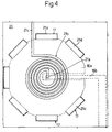
- the second metal layer 21 is shaped, and forms a contact region 21a extending inside the aperture 35; a coil 21b of the inductor extending, spiral-shaped, above the intermediate dielectric layer 20, from the contact region 21a towards the exterior; and a second connection line 21c extending without interruption from the coil 21b, as shown in figure 4, in which broken lines also represent the sacrificial region 16a and the first connection line 16b.
- etch regions 21d are formed, which are approximately in the shape of "plugs", providing the structure in figure 3; in addition (in a known and therefore not shown manner), the second electrical connection level of the circuit is formed.
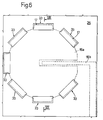
- a passivation layer 25 of dielectric material is deposited and removed selectively at contact pads (not shown) of the circuit and at the etch regions 21d, which remain uncovered, as shown in figure 5.
- a protective layer 26, for example TEOS (tetraethylorthosilicate), with a thickness of 2000 ⁇ is deposited and removed at the etch regions 21d, forming apertures 33 which extend through the protective layer 26 and the passivation layer 25, as shown in figure 6, in which the sacrificial region 16a and the first connection line 16b are again represented by a broken line.
- the metal regions are then wet etched through the apertures 33; thus removing all the etch regions 21d and the sacrificial region 16a below the intermediate dielectric layer 20.
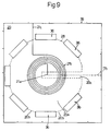
- the protective layer 26 is removed from the entire surface (blanket removal). Then the final structure of fig. 8 is obtained, wherein the coil (indicated at 40) of the inductor is carried by a bracket 20a formed from the intermediate dielectric layer 20, and is supported at the areas 20b which are delimited laterally by the apertures 36, as can be seen in figure 9, which shows a schematic view from above and on a reduced scale of the finished device, wherein the passivation layer 25 has been omitted and the periphery of the air gap 28 and the first connection line 16b are indicated by a broken line. As can be seen, the bracket 20a is also in contact with the wafer 3 at the narrow strip which surrounds the first connection line 16b (above the slot 18, and indicated as a portion of electrical isolation 20c).
- the integrated inductor 40 has a high quality factor, owing to the presence of an air gap, indicated at 28 in figs. 7 and 8, between the bracket 20a and the surface dielectric layer 14, and to the presence of a thick field oxide layer 4, which further reduces the coupling of the inductor and the substrate.
- the production method described is compatible with the usual production processes used in the microelectronics industry, and thus has the advantages of reliability, controllability and repeatability which are typical of these processes. It requires only an additional mask for shaping the protective layer 26, compared with the standard processes with two metal levels, since the first metal level is also used to form the sacrificial region, and the second metal level is used to form the inductor; it therefore has costs which are comparable with, or only slightly higher than those of the standard processes.
Landscapes
- Semiconductor Integrated Circuits (AREA)
Priority Applications (4)
| Application Number | Priority Date | Filing Date | Title |
|---|---|---|---|
| EP97830536A EP0915513A1 (fr) | 1997-10-23 | 1997-10-23 | Bobine intégrée à haut facteur de qualité et son procédé de fabrication |
| US09/170,914 US6437418B1 (en) | 1997-10-23 | 1998-10-13 | High quality factor, integrated inductor and production method thereof |
| JP10301029A JPH11204730A (ja) | 1997-10-23 | 1998-10-22 | 集積化インダクタおよびその製造方法 |
| US09/952,625 US6472257B2 (en) | 1997-10-23 | 2001-09-13 | High quality factor, integrated inductor and production method thereof |
Applications Claiming Priority (1)
| Application Number | Priority Date | Filing Date | Title |
|---|---|---|---|
| EP97830536A EP0915513A1 (fr) | 1997-10-23 | 1997-10-23 | Bobine intégrée à haut facteur de qualité et son procédé de fabrication |
Publications (1)
| Publication Number | Publication Date |
|---|---|
| EP0915513A1 true EP0915513A1 (fr) | 1999-05-12 |
Family
ID=8230819
Family Applications (1)
| Application Number | Title | Priority Date | Filing Date |
|---|---|---|---|
| EP97830536A Withdrawn EP0915513A1 (fr) | 1997-10-23 | 1997-10-23 | Bobine intégrée à haut facteur de qualité et son procédé de fabrication |
Country Status (3)
| Country | Link |
|---|---|
| US (2) | US6437418B1 (fr) |
| EP (1) | EP0915513A1 (fr) |
| JP (1) | JPH11204730A (fr) |
Cited By (4)
| Publication number | Priority date | Publication date | Assignee | Title |
|---|---|---|---|---|
| WO2002039497A1 (fr) * | 2000-11-09 | 2002-05-16 | Telefonaktiebolaget Lm Ericsson | Structure d'inductance de circuit integre et mesure non destructrice de profondeur de gravure |
| EP1081763A3 (fr) * | 1999-08-30 | 2004-05-06 | Chartered Semiconductor Manufacturing Pte Ltd. | Méthode piègeant l'air pour améliorer le facteur qualité (Q) des inducteurs HF dans la technologie CMOS |
| SG108812A1 (en) * | 1999-10-07 | 2005-02-28 | Chartered Semiconductor Mfg | A method to fabricate horizontal air columns underneath metal inductor |
| FR2966284A1 (fr) * | 2010-10-13 | 2012-04-20 | St Microelectronics Crolles 2 | Composant passif isole du substrat |
Families Citing this family (21)
| Publication number | Priority date | Publication date | Assignee | Title |
|---|---|---|---|---|
| JP4956874B2 (ja) * | 2001-08-02 | 2012-06-20 | ソニー株式会社 | 半導体装置及び半導体の製造方法 |
| US6636139B2 (en) * | 2001-09-10 | 2003-10-21 | Taiwan Semiconductor Manufacturing Company | Structure to reduce the degradation of the Q value of an inductor caused by via resistance |
| KR100438160B1 (ko) * | 2002-03-05 | 2004-07-01 | 삼성전자주식회사 | 인덕터와 캐패시터를 갖는 소자 및 그의 제작방법 |
| CA2484794A1 (fr) * | 2002-05-23 | 2003-12-04 | Schott Ag | Materiau vitreux pour applications hautes frequences |
| JP5027992B2 (ja) * | 2002-05-23 | 2012-09-19 | ショット アクチエンゲゼルシャフト | 高周波用途のためのガラス材料 |
| US7919864B2 (en) * | 2003-10-13 | 2011-04-05 | Stmicroelectronics S.A. | Forming of the last metallization level of an integrated circuit |
| US7129561B2 (en) * | 2003-11-19 | 2006-10-31 | International Business Machines Corporation | Tri-metal and dual-metal stacked inductors |
| US7170181B2 (en) * | 2003-11-19 | 2007-01-30 | International Business Machines Corporation | Optimum padset for wire bonding RF technologies with high-Q inductors |
| US6998952B2 (en) * | 2003-12-05 | 2006-02-14 | Freescale Semiconductor, Inc. | Inductive device including bond wires |
| US7005371B2 (en) * | 2004-04-29 | 2006-02-28 | International Business Machines Corporation | Method of forming suspended transmission line structures in back end of line processing |
| JP4842052B2 (ja) * | 2006-08-28 | 2011-12-21 | 富士通株式会社 | インダクタ素子および集積型電子部品 |
| US7524731B2 (en) * | 2006-09-29 | 2009-04-28 | Freescale Semiconductor, Inc. | Process of forming an electronic device including an inductor |
| US7763976B2 (en) * | 2008-09-30 | 2010-07-27 | Freescale Semiconductor, Inc. | Integrated circuit module with integrated passive device |
| CN102087995A (zh) * | 2009-12-04 | 2011-06-08 | 中芯国际集成电路制造(上海)有限公司 | 集成电路电感及其制作方法 |
| US9105634B2 (en) * | 2012-06-29 | 2015-08-11 | Taiwan Semiconductor Manufacturing Company, Ltd. | Voids in interconnect structures and methods for forming the same |
| US10002700B2 (en) | 2013-02-27 | 2018-06-19 | Qualcomm Incorporated | Vertical-coupling transformer with an air-gap structure |
| US9634645B2 (en) | 2013-03-14 | 2017-04-25 | Qualcomm Incorporated | Integration of a replica circuit and a transformer above a dielectric substrate |
| US9449753B2 (en) | 2013-08-30 | 2016-09-20 | Qualcomm Incorporated | Varying thickness inductor |
| US9208938B2 (en) | 2013-10-02 | 2015-12-08 | Globalfoundries Inc. | Inductor structure having embedded airgap |
| US11581398B2 (en) | 2018-09-07 | 2023-02-14 | Lfoundry S.R.L | Method of fabrication of an integrated spiral inductor having low substrate loss |
| JP7244452B2 (ja) | 2020-03-24 | 2023-03-22 | 株式会社東芝 | アイソレータ |
Citations (3)
| Publication number | Priority date | Publication date | Assignee | Title |
|---|---|---|---|---|
| EP0413348A2 (fr) * | 1989-08-18 | 1991-02-20 | Mitsubishi Denki Kabushiki Kaisha | Circuit intégré semi-conducteur |
| WO1994017558A1 (fr) * | 1993-01-29 | 1994-08-04 | The Regents Of The University Of California | Composant monolithique passif |
| EP0812016A1 (fr) * | 1996-06-04 | 1997-12-10 | Harris Corporation | Dispositif semi-conducteur avec une structure de pont d'air et procédé de fabrication |
Family Cites Families (14)
| Publication number | Priority date | Publication date | Assignee | Title |
|---|---|---|---|---|
| US4262399A (en) * | 1978-11-08 | 1981-04-21 | General Electric Co. | Ultrasonic transducer fabricated as an integral park of a monolithic integrated circuit |
| US5162258A (en) * | 1988-10-17 | 1992-11-10 | Lemnios Zachary J | Three metal personalization of application specific monolithic microwave integrated circuit |
| WO1992022820A2 (fr) * | 1991-06-12 | 1992-12-23 | Harris Corporation | Accelerometre a semi-conducteurs et procede de fabrication |
| US5227658A (en) * | 1991-10-23 | 1993-07-13 | International Business Machines Corporation | Buried air dielectric isolation of silicon islands |
| DE4309917A1 (de) * | 1992-03-30 | 1993-10-07 | Awa Microelectronics | Verfahren zur Herstellung von Siliziummikrostrukturen sowie Siliziummikrostruktur |
| US5306659A (en) * | 1993-03-29 | 1994-04-26 | International Business Machines Corporation | Reach-through isolation etching method for silicon-on-insulator devices |
| US5427975A (en) * | 1993-05-10 | 1995-06-27 | Delco Electronics Corporation | Method of micromachining an integrated sensor on the surface of a silicon wafer |
| US5370766A (en) * | 1993-08-16 | 1994-12-06 | California Micro Devices | Methods for fabrication of thin film inductors, inductor networks and integration with other passive and active devices |
| US5438015A (en) * | 1994-05-11 | 1995-08-01 | United Microelectronics Corp. | Silicon-on-insulator technique with buried gap |
| US5825092A (en) * | 1996-05-20 | 1998-10-20 | Harris Corporation | Integrated circuit with an air bridge having a lid |
| US5872489A (en) * | 1997-04-28 | 1999-02-16 | Rockwell Science Center, Llc | Integrated tunable inductance network and method |
| DE69817518D1 (de) * | 1997-07-10 | 2003-10-02 | St Microelectronics Srl | Verfahren zur Herstellung einer integrieten Schaltungsstruktur durch Entfernung einer Opferschicht |
| JP3214441B2 (ja) * | 1998-04-10 | 2001-10-02 | 日本電気株式会社 | 半導体装置及びその製造方法 |
| SG98398A1 (en) * | 2000-05-25 | 2003-09-19 | Inst Of Microelectronics | Integrated circuit inductor |
-
1997
- 1997-10-23 EP EP97830536A patent/EP0915513A1/fr not_active Withdrawn
-
1998
- 1998-10-13 US US09/170,914 patent/US6437418B1/en not_active Expired - Lifetime
- 1998-10-22 JP JP10301029A patent/JPH11204730A/ja active Pending
-
2001
- 2001-09-13 US US09/952,625 patent/US6472257B2/en not_active Expired - Lifetime
Patent Citations (3)
| Publication number | Priority date | Publication date | Assignee | Title |
|---|---|---|---|---|
| EP0413348A2 (fr) * | 1989-08-18 | 1991-02-20 | Mitsubishi Denki Kabushiki Kaisha | Circuit intégré semi-conducteur |
| WO1994017558A1 (fr) * | 1993-01-29 | 1994-08-04 | The Regents Of The University Of California | Composant monolithique passif |
| EP0812016A1 (fr) * | 1996-06-04 | 1997-12-10 | Harris Corporation | Dispositif semi-conducteur avec une structure de pont d'air et procédé de fabrication |
Cited By (6)
| Publication number | Priority date | Publication date | Assignee | Title |
|---|---|---|---|---|
| EP1081763A3 (fr) * | 1999-08-30 | 2004-05-06 | Chartered Semiconductor Manufacturing Pte Ltd. | Méthode piègeant l'air pour améliorer le facteur qualité (Q) des inducteurs HF dans la technologie CMOS |
| SG108812A1 (en) * | 1999-10-07 | 2005-02-28 | Chartered Semiconductor Mfg | A method to fabricate horizontal air columns underneath metal inductor |
| US7573081B2 (en) | 1999-10-07 | 2009-08-11 | Chartered Semiconductor Manufacturing Ltd. | Method to fabricate horizontal air columns underneath metal inductor |
| WO2002039497A1 (fr) * | 2000-11-09 | 2002-05-16 | Telefonaktiebolaget Lm Ericsson | Structure d'inductance de circuit integre et mesure non destructrice de profondeur de gravure |
| US6720229B2 (en) | 2000-11-09 | 2004-04-13 | Telefonaktiebolaget Lm Ericsson (Publ) | Integrated circuit inductor structure and non-destructive etch depth measurement |
| FR2966284A1 (fr) * | 2010-10-13 | 2012-04-20 | St Microelectronics Crolles 2 | Composant passif isole du substrat |
Also Published As
| Publication number | Publication date |
|---|---|
| US20020011653A1 (en) | 2002-01-31 |
| US6472257B2 (en) | 2002-10-29 |
| JPH11204730A (ja) | 1999-07-30 |
| US6437418B1 (en) | 2002-08-20 |
Similar Documents
| Publication | Publication Date | Title |
|---|---|---|
| EP0915513A1 (fr) | Bobine intégrée à haut facteur de qualité et son procédé de fabrication | |
| US8076755B2 (en) | Semiconductor device and method of manufacturing the same | |
| US7452796B2 (en) | Semi-conductor device with inductive component and method of making | |
| US6939788B2 (en) | Semiconductor device with inductive component and method of making | |
| CN100353552C (zh) | 在无线频率集成电路中提供护罩用以降低噪声耦合的一种装置及方法 | |
| US20010028098A1 (en) | Method and structure of manufacturing a high-q inductor with an air trench | |
| US20020016058A1 (en) | Microelectronic air-gap structures and methods of forming the same | |
| US6258688B1 (en) | Method to form a high Q inductor | |
| US8026575B2 (en) | Semiconductor device, electronic device, and manufacturing method of the same | |
| JP2000277693A (ja) | 誘導要素を組み込んだ集積回路及びこのような集積回路を製造する方法 | |
| US6835977B2 (en) | Variable capactor structure | |
| US6518141B2 (en) | Method for manufacturing a radio frequency integrated circuit on epitaxial silicon | |
| US6933229B2 (en) | Method of manufacturing semiconductor device featuring formation of conductive plugs | |
| US20020140050A1 (en) | Semiconductor device having an inductor with low loss | |
| US11735583B2 (en) | Integrated isolator incorporating trench capacitor | |
| US6087252A (en) | Dual damascene | |
| CN117999871A (zh) | 具有电介质侧壁间隔件的金属-绝缘体-金属(mim)电容器模块 | |
| US6316352B1 (en) | Method of fabricating a bottom electrode | |
| JP2007053124A (ja) | 半導体装置 | |
| EP0826234B1 (fr) | Procede de fabrication d'un circuit integre hybride | |
| JP2002368118A (ja) | 半導体装置およびその製造方法 | |
| US20020068437A1 (en) | Method of forming unlanded via |
Legal Events
| Date | Code | Title | Description |
|---|---|---|---|
| PUAI | Public reference made under article 153(3) epc to a published international application that has entered the european phase |
Free format text: ORIGINAL CODE: 0009012 |
|
| AK | Designated contracting states |
Kind code of ref document: A1 Designated state(s): DE FR GB IT |
|
| AX | Request for extension of the european patent |
Free format text: AL;LT;LV;RO;SI |
|
| 17P | Request for examination filed |
Effective date: 19991022 |
|
| AKX | Designation fees paid |
Free format text: DE FR GB IT |
|
| 17Q | First examination report despatched |
Effective date: 20061227 |
|
| STAA | Information on the status of an ep patent application or granted ep patent |
Free format text: STATUS: THE APPLICATION IS DEEMED TO BE WITHDRAWN |
|
| 18D | Application deemed to be withdrawn |
Effective date: 20070709 |