EP0915527B1 - Nichtreziproke Schaltungsanordnung - Google Patents
Nichtreziproke Schaltungsanordnung Download PDFInfo
- Publication number
- EP0915527B1 EP0915527B1 EP98119234A EP98119234A EP0915527B1 EP 0915527 B1 EP0915527 B1 EP 0915527B1 EP 98119234 A EP98119234 A EP 98119234A EP 98119234 A EP98119234 A EP 98119234A EP 0915527 B1 EP0915527 B1 EP 0915527B1
- Authority
- EP
- European Patent Office
- Prior art keywords
- electrode
- capacitor
- circuit device
- nonreciprocal circuit
- board
- Prior art date
- Legal status (The legal status is an assumption and is not a legal conclusion. Google has not performed a legal analysis and makes no representation as to the accuracy of the status listed.)
- Expired - Lifetime
Links
- 239000003990 capacitor Substances 0.000 claims description 151
- 239000000758 substrate Substances 0.000 claims description 40
- 230000002093 peripheral effect Effects 0.000 claims description 35
- 239000011347 resin Substances 0.000 claims description 8
- 229920005989 resin Polymers 0.000 claims description 8
- 239000011810 insulating material Substances 0.000 claims description 3
- 230000002441 reversible effect Effects 0.000 claims description 2
- 230000008054 signal transmission Effects 0.000 claims 1
- 238000012360 testing method Methods 0.000 description 21
- 230000008901 benefit Effects 0.000 description 20
- 238000004519 manufacturing process Methods 0.000 description 13
- 230000008859 change Effects 0.000 description 10
- 230000005540 biological transmission Effects 0.000 description 5
- 238000010276 construction Methods 0.000 description 5
- 230000035882 stress Effects 0.000 description 5
- 230000008030 elimination Effects 0.000 description 4
- 238000003379 elimination reaction Methods 0.000 description 4
- 230000008646 thermal stress Effects 0.000 description 4
- 230000015572 biosynthetic process Effects 0.000 description 3
- 238000000034 method Methods 0.000 description 3
- 238000012545 processing Methods 0.000 description 3
- 230000005855 radiation Effects 0.000 description 3
- 229910000859 α-Fe Inorganic materials 0.000 description 3
- 238000005530 etching Methods 0.000 description 2
- 238000003780 insertion Methods 0.000 description 2
- 230000037431 insertion Effects 0.000 description 2
- 239000002184 metal Substances 0.000 description 2
- 229910052751 metal Inorganic materials 0.000 description 2
- 238000010295 mobile communication Methods 0.000 description 2
- 238000007747 plating Methods 0.000 description 2
- 230000008569 process Effects 0.000 description 2
- 229910000679 solder Inorganic materials 0.000 description 2
- 241000282341 Mustela putorius furo Species 0.000 description 1
- BQCADISMDOOEFD-UHFFFAOYSA-N Silver Chemical compound [Ag] BQCADISMDOOEFD-UHFFFAOYSA-N 0.000 description 1
- 238000004891 communication Methods 0.000 description 1
- 239000012141 concentrate Substances 0.000 description 1
- 239000004020 conductor Substances 0.000 description 1
- 230000001419 dependent effect Effects 0.000 description 1
- 238000010586 diagram Methods 0.000 description 1
- 230000000694 effects Effects 0.000 description 1
- PCHJSUWPFVWCPO-UHFFFAOYSA-N gold Chemical compound [Au] PCHJSUWPFVWCPO-UHFFFAOYSA-N 0.000 description 1
- 239000010931 gold Substances 0.000 description 1
- 229910052737 gold Inorganic materials 0.000 description 1
- 238000009413 insulation Methods 0.000 description 1
- 230000002427 irreversible effect Effects 0.000 description 1
- 230000009467 reduction Effects 0.000 description 1
- 230000004044 response Effects 0.000 description 1
- 229910052709 silver Inorganic materials 0.000 description 1
- 239000004332 silver Substances 0.000 description 1
- 238000005476 soldering Methods 0.000 description 1
- 229910001220 stainless steel Inorganic materials 0.000 description 1
- 239000010935 stainless steel Substances 0.000 description 1
- 238000005382 thermal cycling Methods 0.000 description 1
- 238000007740 vapor deposition Methods 0.000 description 1
Images






Classifications
-
- H—ELECTRICITY
- H01—ELECTRIC ELEMENTS
- H01P—WAVEGUIDES; RESONATORS, LINES, OR OTHER DEVICES OF THE WAVEGUIDE TYPE
- H01P1/00—Auxiliary devices
- H01P1/32—Non-reciprocal transmission devices
- H01P1/38—Circulators
- H01P1/383—Junction circulators, e.g. Y-circulators
- H01P1/387—Strip line circulators
-
- H—ELECTRICITY
- H01—ELECTRIC ELEMENTS
- H01P—WAVEGUIDES; RESONATORS, LINES, OR OTHER DEVICES OF THE WAVEGUIDE TYPE
- H01P1/00—Auxiliary devices
- H01P1/32—Non-reciprocal transmission devices
- H01P1/36—Isolators
-
- H—ELECTRICITY
- H01—ELECTRIC ELEMENTS
- H01P—WAVEGUIDES; RESONATORS, LINES, OR OTHER DEVICES OF THE WAVEGUIDE TYPE
- H01P1/00—Auxiliary devices
- H01P1/32—Non-reciprocal transmission devices
- H01P1/38—Circulators
- H01P1/383—Junction circulators, e.g. Y-circulators
Definitions
- the present invention relates to a nonreciprocal circuit device, such as an isolator, a circulator, etc., used in a microwave band.
- concentrated-constant-type isolators for use in mobile communication apparatuses, such as portable telephones, have functions of allowing a transmission signal to pass only in the transmission direction and preventing transmission thereof in the reverse direction. Also, in recent mobile communication apparatuses, there has been a strong demand for a lower cost as well as a smaller size and a lighter weight from the viewpoint of its use, and in response to this, similarly a smaller size, a lighter weight, and a lower cost are in demand also in the isolator.
- concentrated-constant-type isolators conventionally, there is a concentrated-constant-type isolator of a construction in which, as shown in Fig. 20, a permanent magnet 52, a center electrode body 53, a matching circuit board 54, and a grounding plate 55 are disposed in sequence from the top between upper and lower yokes 50 and 51.
- This center electrode body 53 is constructed in such a way that three center electrodes 57 are placed so as to intersect each other in a circular-plate ferrite 56 in an electrically insulated state.
- the matching circuit board 54 has a circular hole 54b through which the center electrode body 53 is inserted and placed is formed in the central portion of a dielectric substrate 54a in the form of a rectangular thin plate.
- capacitor electrodes 58 are formed to be connected to input/output ports P1 to P3 of each of the center electrodes 57.
- a termination resistance film 59 is connected to the port P3.
- the circular hole 54b must be formed and each capacitor electrode 58 must be pattern-formed in the dielectric substrate 54a of a thin plate. Therefore, processing during manufacture and handling during assembly take time and effort, presenting the problem that the costs are increased.
- portions other than the capacitor electrode 58 cause an increase in area and an increase in weight, presenting the problem that the above-described demand for a smaller size and a lighter weight cannot be met.
- a matching capacitor in place of such a matching circuit board, there is a case in which a single-board-type capacitor is employed such that capacitor electrodes are formed on the entire surface of both sides of a dielectric substrate with the board in between.
- This single-board-type capacitor can be manufactured merely by forming electrodes on both main surfaces of a motherboard made of a large flat plate and by cutting the motherboard to predetermined dimensions, and mass production thereof is possible. For this reason, compared to a conventional case in which circular holes and a plurality of capacitor electrodes are formed on a dielectric substrate, processing and handling are easy, and costs can be reduced. Also, since electrodes are formed on the entire surface of the board, a wasteful increase in area and in weight can be eliminated, and a smaller size and a lighter weight can be achieved by an amount corresponding to the elimination.
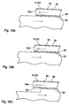
- Figs. 16 to 18 show an example of an isolator employing the single-board-type capacitor.
- the reference numerals which are the same as those of Fig. 20 indicate the same or corresponding components.
- This isolator is constructed such that a circular hole 61 through which a center electrode body 53 is inserted and placed is formed on a bottom wall 60a of a grounding member 60 made of a resin, each of single-board-type capacitors C1 to C3 is disposed in such a manner as to surround the center electrode body 53 around the edge of the circular hole 61, and a single-board-type resistor R is disposed.
- a grounding electrode 63 formed in the grounding member 60 is connected to a capacitor electrode 62 on the cold end side (bottom surface) of each of the single-board-type capacitors C1 to C3, and the input/output ports P1 to P3 of each center electrode 57 are connected to the capacitor electrode 62 on the hot end side (top surface.)
- cold end side means one side of a capacitor electrode to be connected to a grounding electrode and hot end side means another side of the capacitor electrode to be connected to a port electrode (i.e. signal line.)
- the capacitor electrode 62 is positioned up to an edge 64a of a dielectric substrate 64, stress is likely to concentrate in the capacitor electrode 62 at this edge 64a portion, very small cracks are prone to be generated when the motherboard is cut, and the capacitor electrode 62 may be peeled from the dielectric substrate 64.
- the capacitor When, in particular, the capacitor is employed in an isolator, during transmission, heat is generated as a result of insertion loss and consumption of reflection power at the termination resistor.
- the capacitor is subjected to a thermal cycle, such as being cooled again, the problem with electrode peeling is likely to occur.
- JP 07263917 A relates to a irreversible circuit element having three input/output ports and three single plate capacitors connected between the input/output ports and ground.
- EP-A-0 779 673 relates to a non-reciprocal circuit element comprising a first central electrode and a second central electrode, which are disposed on a main surface of a ferret member, so that they intersect with each other in an electrically-insulating state.
- a first input/output port and a second input/output port, which are connected to the ends on one side of both central electrodes and a third input/output port, which is connected to the ends on the other side of the central electrodes are provided and two matching capacitors are connected between the first and second input/output ports and the third input/output port.
- the central conductors are connected to an upper electrode of the matching capacitors.
- EP 0 618 636 A2 relates to a multi-layer circulator including a circulator element and a plurality of terminal electrodes formed on side surfaces of the circulator element. Resonating capacitors are connected to the terminal electrodes formed on the side surfaces of the circulator.
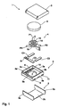
- Figs. 1 to 5 are views illustrating a concentrated-constant-type isolator according to embodiments of the present invention.
- Fig. 1 is an exploded, perspective view showing a single-board-type capacitor.
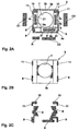
- Figs. 2A to 2C are respectively a top plan view and a bottom plan view of a grounding member, and a see-through view of an electrode pattern.
- Figs. 3 and 4 are respectively a sectional view and a plan view showing a state in which a single-board-type capacitor is connected.
- Fig. 5 is a view showing a method of manufacturing a single-board-type capacitor.
- a concentrated-constant-type isolator 1 of this embodiment is constructed in such a way that a resin grounding member 3 is disposed in a magnetic metal lower yoke 2 having right and left side walls 2a and 2a, and a bottom wall 2b; a center electrode assembly 4 is placed in the grounding member 3; and a box-shaped upper yoke 5 similarly made of a magnetic metal is mounted in the lower yoke 2, forming a magnetic closed circuit. Also, a circular-shaped permanent magnet 6 is attached onto the inner surface of the upper yoke 5, so that a DC magnetic field is applied to the center electrode assembly 4 by the permanent magnet 6.
- the isolator 1 is a rectangular-parallelepiped, the outer shape of which has the plane dimensions 7.5 x 7.5 mm or less and a height of 2.5 mm or less, and is surface-mounted onto a line of a circuit board (not shown).
- the center electrode assembly 4 is of a construction in which three center electrodes 13 to 15 are placed on the top surface of a circular-plate-shaped ferrite 12 in such a manner as to intersect each other with an angle of 120 degrees in an electrically insulated state, the input/output ports P1 to P3 on one end side of each of the center electrodes 13 to 15 are made to project outwards, and a shield section 16 common to each of the center electrodes 13 to 15 on the other end side is brought into abutment with the bottom surface of the ferrite 12, this shield section 16 being connected to the bottom wall 2b of the lower yoke 2.
- the grounding member 3 has a construction in which a bottom wall 3b is integrally formed with side walls 3a in the shape of a rectangular frame, with a circular hole 7 through which the center electrode assembly 4 is inserted and placed being formed in the central portion of the bottom wall 3b.
- Capacitor positioning recesses 3c are each provided around the edge of the circular hole 7 of this bottom wall 3b, and a grounding electrode 8 is formed in the bottom surface of each recess 3c.
- Each of these grounding electrodes 8 is connected to grounding terminals 9 and 9 formed on the outer surfaces of the right and left side walls 3a.
- Input/output port electrodes 10 and 10 are respectively formed on the right and left upper end portions of the bottom wall 3b, and each of the port electrodes 10 is connected to input/output terminals 11 and 11 formed on the outer surfaces of the right and left side walls 3a.
- Each of the grounding terminals 9 and the input/output terminals 11 is surface-mounted onto a line of a circuit board (not shown).
- the single-board-type matching capacitors C1 to C3 are housed and disposed inside each of the positioning recesses 3c. Also, a termination resistor R is placed in parallel with the single-board-type matching capacitor C3 inside the lower-edge positioning recess 3c, and the termination resistor R is connected to the grounding terminal 9.
- each of the single-board-type matching capacitors C1 to C3 is of a construction in which capacitor electrodes 18 and 18 are formed on the entire surface of both main surfaces of a rectangular thin-plate-shaped dielectric substrate 17 in such a manner as to be opposed each other with the substrate 17 in between.
- each of the single-board-type matching capacitors C1 to C3 is manufactured by pattern-forming a silver thick-film electrode 20 on both surfaces of a motherboard 19 made of a large flat plate by a method, such as printing, plating, contact bonding, or vapor deposition, and by cutting the motherboard 19 into predetermined dimensions.
- Each of the grounding electrodes 8 is formed smaller than the capacitor electrode 18 in such a manner as to be positioned inwardly from an outer peripheral edge 18a of the capacitor electrode 18 around the entire outer peripheral edge 8a of the grounding electrode 8.
- the outer peripheral section of the grounding electrode 8 forms a non-connected section 21 to which the capacitor electrode 18 is not connected.
- the capacitor electrode 18 on the cold end side of each of the single-board-type matching capacitors C1 to C3 is soldered and connected to each of the grounding electrodes 8.
- Each of the input/output ports P1 to P3 of each of the center electrodes 13 to 15 is formed so as to be positioned inwardly from an outer peripheral edge 18a of the capacitor electrode 18 of the single-board-type matching capacitors C1 to C3.
- Each of the input/output ports P1 to P3 is soldered and connected to the capacitor electrode 18 on the hot end side.
- Fig. 4 shows an exemplary magnified diagram that input/output port P3 is connected to capacitor electrode 18 on hot end side of capacitor C3 and capacitor electrode 18 of capacitor C3 on cold end side is connected to grounding electrode 8.
- the tip portions of the two ports P1 and P2 of the input/output ports P1 to P3 are connected to the input/output port electrodes 10, and the tip portion of the remaining port P3 is connected to the termination resistor R.
- the concentrated-constant-type isolator 1 of this embodiment since the outer peripheral edge 8a of the grounding electrode 8 to which the capacitor electrode 18 of each of the single-board-type matching capacitors C1 to C3 is connected, and the input/output ports P1 to P3 are formed small so as to be positioned inwardly from the outer peripheral edge 18a of the capacitor electrode 18, electrode peeling in the edge portion of the capacitor electrode 18, in which cracks are likely to occur during stress concentration and manufacture, can be prevented, and reliability with respect to quality can be improved.
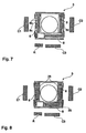
- Figs. 6 to 15 are views illustrating a concentrated-constant-type isolator according to each embodiment of the present invention.
- the reference numerals which are the same as those of Figs. 2 to 4 indicate the same or corresponding components.
- Fig. 6 shows an embodiment of the present invention. This embodiment is constructed such that only both long-side edges 8b of the grounding electrode 8 which are formed rectangular are formed in such a manner as to be positioned inwardly from both long-side edges of the capacitor electrode 18.
- the long-side edges 8b of the grounding electrode 8 are positioned inwardly from the capacitor electrode 18, electrode peeling in the transverse direction in which electrode peeling is likely to occur can be prevented, and an electrode area in the longitudinal direction can be increased. Also, since the long side of the grounding electrode 3 can be lengthened, it is possible to deal with a single-board-type capacitor of a different length.
- Fig. 7 shows an embodiment of the present invention.
- This embodiment is constructed such that both long-side edges 8b of a capacitcr electrode 8 are positioned inwardly from both long-side edges of a grounding electrode 18, and a central portion 8c along the longitudinal direction of the long-side edge 8b is extended and formed up to the edge of the capacitor electrode 18. Also in this embodiment, while preventing electrode peeling in the transverse direction in which electrode peeling is likely to occur, the electrode area can be increased.
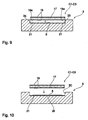
- Figs. 8 and 9 show an embodiment of the present invention. This embodiment is constructed such that an insulating film 25 is coated and formed on a non-connected section 21 of each grounding electrode 8 by printing an insulating resin, and an outer peripheral edge 18a of a capacitor electrode 18 of each of the single-board-type matching capacitors C1 to C3 is brought into contact with this insulating film 25.
- the insulating film 25 formed by a resin is coated onto the non-connected section 21, insulation of the outer peripheral edge 18a of the capacitor electrode 18 can be reliably ensured, making it possible to further prevent electrode peeling.
- This makes it possible to decrease grounding impedance of the isolator 1, to reduce unwanted radiation by an amount corresponding to the decrease in insertion loss, to improve harmonic wave elimination capability, leading to higher performance when the isolator is employed in a communication apparatus, and a stable operation can be obtained.
- the insulating film 25 is not limited to a resin, and other insulating materials can be coated.
- Fig. 10 shows a concentrated-constant-type isolator according to an embodiment of the present invention.
- This isolator is constructed such that an insulating film 26 is coated and formed on the entire bottom surface of the housing recess 3c, and a grounding electrode 8 is formed over the insulating film 26.
- Stainless steel is employed for this insulating film 26, and gold plating is employed for the grounding electrode 8.
- the grounding electrode 8 is formed over the insulating film 26 coated as a base, portions other than the grounding electrode 8 become the insulating film 26. Therefore, the formation of the insulating film 26 is easy in a case in which the shape or the like of the grounding electrode 8 becomes complex, and, similarly to that described above, electrode peeling can be reliably prevented, unwanted radiation can be reduced, and harmonic wave elimination performance can be improved.
- Figs. 11 to 13 show a concentrated-constant-type isolator according to an embodiment of the present invention.
- This isolator is constructed such that a step-down section 3d is formed in a portion corresponding to the non-connected section 21 of the recess 3c of the grounding member 3 in such a manner as to be away from an outer peripheral edge 18a of a capacitor electrode 18.
- the step-down section 3d is formed in a portion corresponding to the non-connected section 21, the outer peripheral edge 18a of the capacitor electrode 18 does not come into contact, making it possible to prevent electrode peeling in a case in which the grounding electrode 8 is formed on the entire surface inside the recess 3c.
- Figs. 14 and 15 show a concentrated-constant-type isolator according to an embodiment of the present invention.
- This isolator is constructed such that a non-connected section 30 defines a portion of the dielectric substrate 17 is exposed and a capacitor electrode is not formed thereon, the non-connected section 30 is formed around the outer peripheral edge of the dielectric substrate 17 of each of the single-board-type matching capacitors C1 to C3, and as a result, the outer peripheral edge 18b of the capacitor electrode 18 is positioned inwardly from the outer peripheral edge 8c of the grounding electrode 8.
- this non-connected section 30 can be realized by forming the capacitor electrode 18 in a portion excluding the non-connected section 30 of the dielectric substrate 17 by printing, or by removing the outer peripheral edge of the electrode formed on the entire surface of the dielectric substrate 17 by etching.
- the non-connected section 30 is formed around the outer peripheral edge of the dielectric substrate 17 of each of the single-board-type matching capacitors C1 to C3, and since no electrodes are disposed in the edge portion of the dielectric substrate 17 where cracks are likely to occur during stress concentration and manufacture, it is possible to prevent electrode peeling in the edge portion and to improve reliability with respect to quality.
- a feature of the isolator of this embodiment is that the thickness of a dielectric substrate 17 of each of the above-described single-board-type capacitors C1, C2, and C3 is 0.5 mm or less, and that the film thickness of a capacitor electrode 18 is 0.05 mm or less (see Figs. 3, 9, 10, 13, and 15).
- the thickness of the dielectric substrate 17 of the single-board-type capacitors C1, C2, and C3 is 0.5 mm or less, it is possible to form the single-board-type capacitors C1, C2, and C3 into a smaller size and a thinner plate without causing electrode peeling, thereby contributing to an even smaller size of the isolator.
- the thickness of the dielectric substrate in a conventional case in which the entire surface of the electrode is soldered, in order to obtain a required capacitance value while preventing electrode peeling, the thickness of the dielectric substrate must be, for example, 1 mm or more, presenting the problem that the capacitor becomes larger.
- the film thickness of the capacitor electrode 18 of each of the single-board-type capacitors C1, C2, and C3 being set to 0.05 mm or less, the problem with electrode peeling when the thickness of the dielectric substrate 17 is 0.5 mm or less can be prevented more reliably.
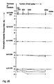
- a single-board-type capacitor was used, in which the thickness td of the dielectric substrate D was varied, the entire surface of a capacitor electrode E on one side of each single-board-type capacitor was soldered and connected to a Cu board 70 as a connected electrode, and a heat cycle test was carried out in this state. Then, the change rate of the electrostatic capacity value between the capacitor electrode E on the non-soldered side and the Cu board 70 was checked (see the ⁇ marks in Fig. 21).
- the thicknesses td of the respective dielectric substrate D were 0.1, 0.2, 0.5, and 1.0 mm.
- the capacitor electrode E an Ag thick film electrode was used, and the film thickness of the electrode E was 0.02 mm.
- the solder thickness ta for connecting was 0.01 to 0.02 mm, and the thickness of the Cu board 70 was 0.2 mm.
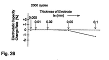
- a single-board-type capacitor as a product of the present invention was used, in which the film thickness te of the capacitor electrode E was varied, Cu boards 71 and 71 were soldered and connected to both sides of the capacitor electrode E of each single-board-type capacitor in such a manner as to be positioned inwardly from the outer peripheral edge of the capacitor electrode E, and a heat cycle test was carried out in this state, so that the change rate of the electrostatic capacity value was checked in the same way as in test 1 described above.
- Single-board-type capacitors each having a size of length 3 mm x width 1 mm were used (see the plan view of Fig. 22B).
- the film thicknesses te of the respective capacitor electrodes E were 0.005, 0.01, 0.02, 0.05, and 0.1 mm.
- the thickness td of the dielectric board D was 0.2 mm.
- the solder thickness ta for connecting, and the thickness tb of the Cu board 71 were of the same thickness as that of test 1 described above.
- Figs. 23 and 24, and Figs. 25 and 26 are characteristic views showing the test results of tests 1 and 2, respectively.
- the O mark indicates the maximum or minimum value
- the • mark indicates the average value thereof.
- Figs. 24 and 26 are characteristic views in which the change rate of the electrostatic capacity value in 2,000 cycles of tests 1 and 2 is summarized, respectively.
- the results of test 1 reveal that, when the substrate thickness td is 0.1 or 0.2 mm, the electrostatic capacity change rate is as large as -1.4% and -1.2% (see the • marks in the figure) in terms of average value, and also indicate the occurrence of electrode peeling. Also, when the substrate thickness td is 0.5 or 1.0 mm, the change rate during 2,000 heat cycles is as low as -0.3% and -0.05% in terms of average value, and the larger the substrate thickness td becomes, the more unlikely it is for electrode peeling to occur. However, the capacitor becomes larger by an amount corresponding to an increase in the thickness td of the dielectric substrate D, thus making it impossible to achieve a smaller size of the isolator.
- the film thickness te of the capacitor electrode E when the film thickness te of the capacitor electrode E is 0.1 mm, the electrostatic capacity during 2,000 heat cycles changes greatly to -1.0% (see the • marks in the figure). This becomes nearly the same as that in which the entire surface of the capacitor electrode is soldered to a thick Cu board, and this is considered to cause electrode peeling to easily occur because of the thermal stress resulting from the difference in the thermal expansion coefficients.
- the setting of the film thickness te of the capacitor electrode E at 0.1 mm is difficult in practice in consideration of cost and manufacturing time and labor, because this results in a thickness that is half the thickness td of the dielectric substrate D.
- the results of tests 1 and 2 show that as a result of the thickness td of the dielectric substrate D of the single-board-type capacitor being set to 0.5 mm or less and the film thickness te of the capacitor electrode E being set to 0.05 mm or less, the capacitor can be formed into a smaller size and a thinner plate without causing a problem with electrode peeling, contributing to an even smaller size of the isolator.
- the thickness td of the dielectric substrate D be in a range of 0.1 to 0.5 mm and the film thickness te of the capacitor electrode E be in a range of 0.005 to 0.05 mm.
- the nonreciprocal circuit device of the present invention since at least a part of the outer peripheral edge of a connected electrode, to which the cold end side of the capacitor electrode of the single-board-type capacitor is connected, is positioned inwardly from the outer peripheral edge of the capacitor electrode, there is the advantages that electrode peeling in the edge portion of a capacitor electrode, in which cracks are likely to occur during stress concentration and manufacture, can be prevented, and reliability with respect to quality can be improved. Furthermore, since the edge portion of a capacitor electrode is not connected even if thermal stress due to a difference in the thermal expansion coefficients occurs, there is the advantage that, also from this point, electrode peeling can be prevented.
- the outer peripheral edge of the connected electrode is positioned inwardly from the outer peripheral edge of the capacitor electrode around the entire periphery of the connected electrode, there is the advantage that electrode peeling can be reliably prevented.
- the capacitor electrode and the connected electrode are formed rectangular, and the long-side edge of the connected electrode is positioned inwardly from the long-side edge of the capacitor electrode, there is the advantage that electrode peeling in the transverse direction in which electrode peeling is likely to occur can be prevented, and an electrode area in the longitudinal direction can be increased. Also, there is the advantage that it is possible to deal with a capacitor of a different length.
- the insulating film is formed by printing a resin, there is the advantage that the insulating film can easily be formed with high accuracy.
- the outer peripheral edge of the capacitor electrode can be placed in a non-contact state, yielding the advantage that electrode peeling can be prevented more reliably.
- the capacitor electrode is formed by printing, there is the advantage that a non-connected section around the edge of the dielectric substrate can be easily formed.
- a single-board-type capacitor is manufactured in such a way that electrodes are pattern-formed on both main surfaces of a dielectric motherboard in such a manner as to be opposed each other with the motherboard in between and the motherboard is cut to predetermined dimensions, manufacturing becomes easy and mass production is possible, yielding the advantage that the costs of parts can be reduced, and a wasteful increase in area and in weight can be eliminated, contributing to a smaller size and a lighter weight.
- the thickness of the dielectric substrate of the single-board-type capacitor is 0.5 mm or less, the entire capacitor can be formed smaller and thinner without causing a problem with electrode peeling, thereby contributing to an even smaller size of the isolator.
- the film thickness of the capacitor electrode of the single-board-type capacitor is 0.05 mm, there is the advantage that the problem with electrode peeling when the thickness of the dielectric substrate is 0.5 mm or less can be prevented more reliably.
Landscapes
- Non-Reversible Transmitting Devices (AREA)
Claims (14)
- Eine nichtreziproke Schaltungsvorrichtung, die Charakteristika aufweist, derart, dass eine Dämpfung in die Richtung einer Signalsendung gering ist und eine Dämpfung in die umgekehrte Richtung groß ist, und die Anpassungskondensatoren aufweist, die in Signal-Eingang/Ausgang-Toren (P1, P2, P3) angeordnet sind,
wobei die Anpassungskondensatoren aus Einzelplatinentyp-Kondensatoren (C1, C2, C3) gebildet sind, die Kondensatorelektroden (18) umfassen, die gebildet sind, um einander an der gesamten Oberfläche beider Hauptoberflächen eines dielektrischen Substrats (17) mit dem Substrat dazwischen gegenüberzuliegen, dadurch gekennzeichnet, dass zumindest ein Teil der äußeren peripheren Kante (8a; 8b; 8b, 8c) einer Masseelektrode (8) der nichtreziproken Schaltungsvorrichtung, mit der die Masseseitenelektrode der Kondensatorelektroden (18) des Einzelplatinentyp-Kondensators (C1, C2, C3) verbunden ist, einwärts von der äußeren peripheren Kante (18a) der Kondensatorelektrode (18) positioniert ist. - Eine nichtreziproke Schaltungsvorrichtung gemäß Anspruch 1, bei der zumindest ein Teil der äußeren peripheren Kante einer Torelektrode (P1, P2, P3) der nichtreziproken Schaltungsvorrichtung, mit der die Torleitungsseitenelektrode der Kondensatorelektroden (18) des Einzelplatinentyp-Kondensators (C1, C2, C3) verbunden ist, einwärts von der äußeren peripheren Kante (18a) der Kondensatorelektrode (18) positioniert ist.
- Eine nichtreziproke Schaltungsvorrichtung gemäß einem der Ansprüche 1 und 2, bei der die äußere periphere Kante (8a) der Masseelektrode (8) von der äußeren peripheren Kante (18a) der Masseseitenkondensatorelektrode (18) einwärts um die gesamte Peripherie der Masseelektrode (8) herum positioniert ist.
- Eine nichtreziproke Schaltungsvorrichtung gemäß einem der Ansprüche 1 und 2, bei der die Kondensatorelektrode (18) und die Masseelektrode (8) rechteckig gebildet sind und die Langseitenkante (8b) der Masseelektrode (8) von der Langseitenkante der Kondensatorelektrode (18) einwärts positioniert ist.
- Eine nichtreziproke Schaltungsvorrichtung gemäß Anspruch 4, bei der ein Teil (8c) der Langseitenkante (8b) der Masseelektrode (8) erweitert ist und bis zu der Langseitenkante der Kondensatorelektrode (18) gebildet ist.
- Eine nichtreziproke Schaltungsvorrichtung gemäß einem der Ansprüche 1 und 2, bei der ein nichtverbundener Abschnitt (21) an der Außenseite der Masseelektrode (8) mit einem isolierenden Film (25) bedeckt ist, der aus einem isolierenden Material hergestellt ist.
- Eine nichtreziproke Schaltungsvorrichtung gemäß Anspruch 6, bei der der isolierende Film (25), der aus einem Harz hergestellt ist, bedeckt ist.
- Eine nichtreziproke Schaltungsvorrichtung gemäß Anspruch 7, bei der der isolierende Film (25) durch ein Drucken eines Harzes gebildet ist.
- Eine nichtreziproke Schaltungsvorrichtung gemäß Anspruch 6, bei der die Masseelektrode (8) über einem isolierenden Film (26) gebildet ist, der als eine Basis beschichtet ist.
- Eine nichtreziproke Schaltungsvorrichtung gemäß einem der Ansprüche 1 und 2, bei der ein nichtverbundener Abschnitt (21) an der Außenseite der Masseelektrode (8) auf eine derartige Weise herabgestuft gebildet ist, um von der äußeren peripheren Kante (18a) der Masseseitenkondensatorelektrode (18) weg zu sein.
- Eine nichtreziproke Schaltungsvorrichtung gemäß einem der Ansprüche 1 bis 10, bei der ein Einzelplatinentyp-Kondensator (C1, C2, C3) auf eine derartige Weise hergestellt ist, dass Elektroden an beiden Hauptoberflächen einer dielektrischen Hauptplatine auf eine derartige Weise strukturiert sind, um einander mit der Hauptplatine dazwischen gegenüberzuliegen, und die Hauptplatine auf vorbestimmte Abmessungen geschnitten ist.
- Eine nichtreziproke Schaltungsvorrichtung gemäß einem der Ansprüche 1 bis 10, bei der ein Einzelplatinentyp-Kondensator (C1, C2, C3) und ein Massebauglied, wobei die Masseelektrode (8) an demselben gebildet ist, integriert in einem Zustand zusammengefügt sind, in dem dieselben miteinander verbunden sind.
- Eine nichtreziproke Schaltungsvorrichtung gemäß einem der Ansprüche 1 bis 12, bei der die Dicke des dielektrischen Substrats (17) des Einzelplatinentyp-Kondensators (C1, C2, C3) 0,5 mm oder weniger beträgt.
- Eine nichtreziproke Schaltungsvorrichtung gemäß einem der Ansprüche 1 bis 13, bei der die Filmdicke der Kondensatorelektrode (18) des Einzelplatinentyp-Kondensators (C1, C2, C3) 0,05 mm oder weniger beträgt.
Priority Applications (1)
| Application Number | Priority Date | Filing Date | Title |
|---|---|---|---|
| EP04016765A EP1473797B1 (de) | 1997-10-13 | 1998-10-12 | Nichtreziproke Schaltungsanordnung |
Applications Claiming Priority (6)
| Application Number | Priority Date | Filing Date | Title |
|---|---|---|---|
| JP27883697 | 1997-10-13 | ||
| JP27883697 | 1997-10-13 | ||
| JP278836/97 | 1997-10-13 | ||
| JP26160298A JP3646532B2 (ja) | 1997-10-13 | 1998-09-16 | 非可逆回路素子 |
| JP261602/98 | 1998-09-16 | ||
| JP26160298 | 1998-09-16 |
Related Child Applications (1)
| Application Number | Title | Priority Date | Filing Date |
|---|---|---|---|
| EP04016765A Division EP1473797B1 (de) | 1997-10-13 | 1998-10-12 | Nichtreziproke Schaltungsanordnung |
Publications (3)
| Publication Number | Publication Date |
|---|---|
| EP0915527A2 EP0915527A2 (de) | 1999-05-12 |
| EP0915527A3 EP0915527A3 (de) | 2000-12-20 |
| EP0915527B1 true EP0915527B1 (de) | 2005-04-20 |
Family
ID=26545152
Family Applications (2)
| Application Number | Title | Priority Date | Filing Date |
|---|---|---|---|
| EP98119234A Expired - Lifetime EP0915527B1 (de) | 1997-10-13 | 1998-10-12 | Nichtreziproke Schaltungsanordnung |
| EP04016765A Expired - Lifetime EP1473797B1 (de) | 1997-10-13 | 1998-10-12 | Nichtreziproke Schaltungsanordnung |
Family Applications After (1)
| Application Number | Title | Priority Date | Filing Date |
|---|---|---|---|
| EP04016765A Expired - Lifetime EP1473797B1 (de) | 1997-10-13 | 1998-10-12 | Nichtreziproke Schaltungsanordnung |
Country Status (6)
| Country | Link |
|---|---|
| US (1) | US6037844A (de) |
| EP (2) | EP0915527B1 (de) |
| JP (1) | JP3646532B2 (de) |
| KR (1) | KR100293682B1 (de) |
| CN (1) | CN1149705C (de) |
| DE (2) | DE69836288T2 (de) |
Families Citing this family (13)
| Publication number | Priority date | Publication date | Assignee | Title |
|---|---|---|---|---|
| JP3438683B2 (ja) * | 1999-11-30 | 2003-08-18 | 株式会社村田製作所 | 非可逆回路素子、通信装置および非可逆回路素子の製造方法 |
| KR100328257B1 (ko) * | 1999-12-16 | 2002-03-16 | 이형도 | 비가역 회로소자 |
| KR100352489B1 (ko) | 1999-12-16 | 2002-09-11 | 삼성전기주식회사 | 비가역 회로소자 |
| JP2001326503A (ja) * | 2000-05-17 | 2001-11-22 | Murata Mfg Co Ltd | 非可逆回路素子及び通信装置 |
| JP2002261512A (ja) * | 2001-03-01 | 2002-09-13 | Murata Mfg Co Ltd | 非可逆回路素子、通信装置及び非可逆回路素子の製造方法 |
| JP2002314306A (ja) | 2001-04-13 | 2002-10-25 | Murata Mfg Co Ltd | 非可逆回路素子及び通信装置 |
| JP2002368553A (ja) * | 2001-06-08 | 2002-12-20 | Mitsubishi Electric Corp | 高周波増幅器およびそれを用いた無線送信装置 |
| JP2003087014A (ja) * | 2001-06-27 | 2003-03-20 | Murata Mfg Co Ltd | 非可逆回路素子および通信装置 |
| JP4422933B2 (ja) * | 2001-09-05 | 2010-03-03 | 三菱電機株式会社 | 樹脂封止型半導体装置 |
| JP3686884B2 (ja) * | 2002-06-06 | 2005-08-24 | アルプス電気株式会社 | 電子部品用筐体の製造方法 |
| KR20170017061A (ko) | 2015-08-05 | 2017-02-15 | 최종관 | 파라솔지주 고정구 |
| CN111129676B (zh) * | 2020-01-14 | 2022-01-21 | 中国电子科技集团公司第九研究所 | 一种提高环行器谐波抑制性能的方法及环行器 |
| CN113839164B (zh) * | 2021-10-15 | 2022-08-12 | 散裂中子源科学中心 | 一种大功率y结型波导环形器 |
Family Cites Families (8)
| Publication number | Priority date | Publication date | Assignee | Title |
|---|---|---|---|---|
| DE69424819T2 (de) * | 1993-03-31 | 2000-12-07 | Tdk Corp., Tokio/Tokyo | Mehrschichtiger Mikrowellenzirkulator |
| JPH07263917A (ja) * | 1994-03-24 | 1995-10-13 | Murata Mfg Co Ltd | 非可逆回路素子 |
| JPH088612A (ja) * | 1994-06-21 | 1996-01-12 | Tokin Corp | 非可逆回路素子 |
| JPH0936610A (ja) * | 1995-07-25 | 1997-02-07 | Tokin Corp | 非可逆回路素子 |
| JP3264194B2 (ja) * | 1995-12-13 | 2002-03-11 | 株式会社村田製作所 | 非可逆回路素子 |
| JPH09213523A (ja) * | 1996-02-01 | 1997-08-15 | Murata Mfg Co Ltd | 非可逆回路素子 |
| CA2214617C (en) * | 1996-09-06 | 2000-12-19 | Toshihiro Makino | Nonreciprocal circuit device |
| JPH10327003A (ja) * | 1997-03-21 | 1998-12-08 | Murata Mfg Co Ltd | 非可逆回路素子及び複合電子部品 |
-
1998
- 1998-09-16 JP JP26160298A patent/JP3646532B2/ja not_active Expired - Fee Related
- 1998-10-12 DE DE69836288T patent/DE69836288T2/de not_active Expired - Lifetime
- 1998-10-12 EP EP98119234A patent/EP0915527B1/de not_active Expired - Lifetime
- 1998-10-12 DE DE69829823T patent/DE69829823T2/de not_active Expired - Lifetime
- 1998-10-12 EP EP04016765A patent/EP1473797B1/de not_active Expired - Lifetime
- 1998-10-13 CN CNB981209769A patent/CN1149705C/zh not_active Expired - Fee Related
- 1998-10-13 KR KR1019980042736A patent/KR100293682B1/ko not_active Expired - Fee Related
- 1998-10-13 US US09/170,909 patent/US6037844A/en not_active Expired - Lifetime
Also Published As
| Publication number | Publication date |
|---|---|
| US6037844A (en) | 2000-03-14 |
| KR19990037050A (ko) | 1999-05-25 |
| EP1473797A3 (de) | 2004-12-01 |
| EP1473797A2 (de) | 2004-11-03 |
| EP1473797B1 (de) | 2006-10-25 |
| DE69829823T2 (de) | 2006-02-23 |
| KR100293682B1 (ko) | 2001-10-26 |
| CN1216872A (zh) | 1999-05-19 |
| JPH11186814A (ja) | 1999-07-09 |
| CN1149705C (zh) | 2004-05-12 |
| EP0915527A3 (de) | 2000-12-20 |
| DE69836288T2 (de) | 2007-02-15 |
| JP3646532B2 (ja) | 2005-05-11 |
| EP0915527A2 (de) | 1999-05-12 |
| DE69829823D1 (de) | 2005-05-25 |
| DE69836288D1 (de) | 2006-12-07 |
Similar Documents
| Publication | Publication Date | Title |
|---|---|---|
| US6914496B2 (en) | Center-electrode assembly and manufacturing method therefor, nonreciprocal circuit device and communication apparatus using the same | |
| EP0915527B1 (de) | Nichtreziproke Schaltungsanordnung | |
| JPH0818187A (ja) | 電子部品及びその製造方法 | |
| US6559732B2 (en) | Nonreciprocal circuit device with main surfaces of the ferrite and magnet perpendicular to the mounting substrate | |
| US5057804A (en) | Dielectric resonator circuit | |
| US6741478B2 (en) | Compact electronic circuit unit having circulator, manufactured with high productivity | |
| KR100397740B1 (ko) | 비가역 회로소자 및 통신 장치 | |
| US20060022766A1 (en) | High frequency circuit module having non-reciprocal circuit element | |
| US6935002B1 (en) | Method of manufacturing a nonreciprocal circuit device | |
| US6710672B2 (en) | Nonreciprocal circuit device, communication apparatus, and method for manufacturing nonreciprocal circuit device | |
| JP3204423B2 (ja) | 非可逆回路素子 | |
| JP3395748B2 (ja) | 非可逆回路素子及び通信機装置 | |
| US6603370B2 (en) | Nonreciprocal circuit device with a casing average surface roughness less than or equal to 0.9 microns | |
| JP3852434B2 (ja) | 非可逆回路素子および通信装置 | |
| US6796840B2 (en) | Surface mounting type non-reversible circuit element having superior productivity | |
| JP3714220B2 (ja) | 非可逆回路素子及び通信装置 | |
| JP3660316B2 (ja) | 非可逆回路素子 | |
| JP2003017906A (ja) | 非可逆回路素子及び通信装置 | |
| JP3017917B2 (ja) | 誘電体共振器 | |
| JP2006094289A (ja) | 非可逆回路素子 | |
| JP2002319805A (ja) | 中心電極組立体、非可逆回路素子、通信装置及び中心電極組立体の製造方法 | |
| US20100182095A1 (en) | Non-reciprocal circuit device | |
| JPH04103201A (ja) | 誘電体帯域阻止フィルタ | |
| JP2001127505A (ja) | 非可逆回路素子及び通信機装置 | |
| JP2002151914A (ja) | 非可逆回路素子及び通信装置 |
Legal Events
| Date | Code | Title | Description |
|---|---|---|---|
| PUAI | Public reference made under article 153(3) epc to a published international application that has entered the european phase |
Free format text: ORIGINAL CODE: 0009012 |
|
| 17P | Request for examination filed |
Effective date: 19981012 |
|
| AK | Designated contracting states |
Kind code of ref document: A2 Designated state(s): DE FR GB |
|
| AX | Request for extension of the european patent |
Free format text: AL;LT;LV;MK;RO;SI |
|
| PUAL | Search report despatched |
Free format text: ORIGINAL CODE: 0009013 |
|
| AK | Designated contracting states |
Kind code of ref document: A3 Designated state(s): AT BE CH CY DE DK ES FI FR GB GR IE IT LI LU MC NL PT SE |
|
| AX | Request for extension of the european patent |
Free format text: AL;LT;LV;MK;RO;SI |
|
| AKX | Designation fees paid |
Free format text: DE FR GB |
|
| 17Q | First examination report despatched |
Effective date: 20040504 |
|
| GRAP | Despatch of communication of intention to grant a patent |
Free format text: ORIGINAL CODE: EPIDOSNIGR1 |
|
| GRAS | Grant fee paid |
Free format text: ORIGINAL CODE: EPIDOSNIGR3 |
|
| GRAA | (expected) grant |
Free format text: ORIGINAL CODE: 0009210 |
|
| AK | Designated contracting states |
Kind code of ref document: B1 Designated state(s): DE FR GB |
|
| REG | Reference to a national code |
Ref country code: GB Ref legal event code: FG4D |
|
| REF | Corresponds to: |
Ref document number: 69829823 Country of ref document: DE Date of ref document: 20050525 Kind code of ref document: P |
|
| PLBE | No opposition filed within time limit |
Free format text: ORIGINAL CODE: 0009261 |
|
| STAA | Information on the status of an ep patent application or granted ep patent |
Free format text: STATUS: NO OPPOSITION FILED WITHIN TIME LIMIT |
|
| ET | Fr: translation filed | ||
| 26N | No opposition filed |
Effective date: 20060123 |
|
| REG | Reference to a national code |
Ref country code: FR Ref legal event code: PLFP Year of fee payment: 18 |
|
| PGFP | Annual fee paid to national office [announced via postgrant information from national office to epo] |
Ref country code: GB Payment date: 20151021 Year of fee payment: 18 Ref country code: DE Payment date: 20151022 Year of fee payment: 18 |
|
| PGFP | Annual fee paid to national office [announced via postgrant information from national office to epo] |
Ref country code: FR Payment date: 20151023 Year of fee payment: 18 |
|
| REG | Reference to a national code |
Ref country code: DE Ref legal event code: R119 Ref document number: 69829823 Country of ref document: DE |
|
| GBPC | Gb: european patent ceased through non-payment of renewal fee |
Effective date: 20161012 |
|
| REG | Reference to a national code |
Ref country code: FR Ref legal event code: ST Effective date: 20170630 |
|
| PG25 | Lapsed in a contracting state [announced via postgrant information from national office to epo] |
Ref country code: DE Free format text: LAPSE BECAUSE OF NON-PAYMENT OF DUE FEES Effective date: 20170503 Ref country code: FR Free format text: LAPSE BECAUSE OF NON-PAYMENT OF DUE FEES Effective date: 20161102 Ref country code: GB Free format text: LAPSE BECAUSE OF NON-PAYMENT OF DUE FEES Effective date: 20161012 |