EP0915530B1 - Polarisationsselektionschaltung - Google Patents
Polarisationsselektionschaltung Download PDFInfo
- Publication number
- EP0915530B1 EP0915530B1 EP98308588A EP98308588A EP0915530B1 EP 0915530 B1 EP0915530 B1 EP 0915530B1 EP 98308588 A EP98308588 A EP 98308588A EP 98308588 A EP98308588 A EP 98308588A EP 0915530 B1 EP0915530 B1 EP 0915530B1
- Authority
- EP
- European Patent Office
- Prior art keywords
- frequency
- microstrip line
- signal
- amplifying element
- input terminal
- Prior art date
- Legal status (The legal status is an assumption and is not a legal conclusion. Google has not performed a legal analysis and makes no representation as to the accuracy of the status listed.)
- Expired - Lifetime
Links
Images

Classifications
-
- H—ELECTRICITY
- H01—ELECTRIC ELEMENTS
- H01Q—ANTENNAS, i.e. RADIO AERIALS
- H01Q13/00—Waveguide horns or mouths; Slot antennas; Leaky-waveguide antennas; Equivalent structures causing radiation along the transmission path of a guided wave
- H01Q13/02—Waveguide horns
-
- H—ELECTRICITY
- H01—ELECTRIC ELEMENTS
- H01P—WAVEGUIDES; RESONATORS, LINES, OR OTHER DEVICES OF THE WAVEGUIDE TYPE
- H01P1/00—Auxiliary devices
- H01P1/20—Frequency-selective devices, e.g. filters
- H01P1/213—Frequency-selective devices, e.g. filters combining or separating two or more different frequencies
-
- H—ELECTRICITY
- H01—ELECTRIC ELEMENTS
- H01Q—ANTENNAS, i.e. RADIO AERIALS
- H01Q21/00—Antenna arrays or systems
- H01Q21/24—Combinations of antenna units polarised in different directions for transmitting or receiving circularly and elliptically polarised waves or waves linearly polarised in any direction
Definitions
- the present invention relates to a signal selecting circuit for use with a satellite broadcasting reception converter installed in the outdoors.
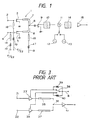
- a conventional signal selecting circuit will be described with reference to FIG. 3.
- a first reception signal e.g. vertically-polarized satellite broadcasting signal
- a second reception signal e.g. horizontally-polarized satellite broadcasting signal
- the first reception signal is amplified by a first high-frequency amplifier 33
- the second reception signal is amplified by a second high-frequency amplifier 34.
- the first high-frequency amplifier 33 and a common output terminal 36; and the second high-frequency amplifier 34 and the common output terminal 36 are connected by a first microstrip line 35 and a second microstrip line 37, respectively.
- the first reception signal amplified by the first high-frequency amplifier 33 is outputted through the first microstrip line 35 to the common output terminal 36
- the second reception signal amplified by the second high-frequency amplifier 34 is outputted through the second microstrip line 37 to the common output terminal 36.
- the first microstrip line 35 and the second microstrip line 37 have a predetermined characteristic impedance, and the lengths thereof are set to 1/2 wavelength of frequencies of the first reception signal and the second reception signal which are respectively transmitted through the first microstrip line 35 and the second microstrip line 37.
- a DC voltage B is supplied through a switch 38 to the first high-frequency amplifier 33 or the second high-frequency amplifier 34. That is, when the first reception signal is received, the switch 38 allows the DC voltage B to be supplied to the first high-frequency amplifier 33 to set the first high-frequency amplifier 33 in the operable state, whereby the first reception signal inputted to the first input terminal 31 is amplified by the first high-frequency amplifier 33 and then supplied through the first microstrip line 35 to the common output terminal 36.
- the second high-frequency amplifier 34 is de-energized by a low DC voltage applied thereto through a resistor 40. As a consequence, the second reception signal inputted to the second input terminal 32 is not amplified but attenuated by the second high-frequency amplifier 34.
- the impedance of the second microstrip line 37 increases as seen from the common output terminal 36, and hence the second reception signal is not delivered to the common output terminal 36. Accordingly, only the first reception signal is inputted to the subsequent amplifier 41.
- the switch 38 allows the DC voltage B to be supplied to the second high-frequency amplifier 34 to set the second high-frequency amplifier 33 to the operable state, whereby the second reception signal inputted to the second input terminal 32 is amplified by the second high-frequency amplifier 33 and then supplied through the second microstrip line 37 to the common output terminal 36.
- the first high-frequency amplifier 33 is de-energized by the Low DC voltage applied thereto through a resistor 39.
- the first reception signal inputted to the first input terminal 31 is not amplified but attenuated by the first high-frequency amplifier 33.
- the length of the first microstrip line 35 is set to the 1/2 wavelength, the impedance of the first microstrip line 35 increases as seen from the common output terminal 36, and hence the first reception signal is not delivered to the common output terminal 36. Accordingly, only the second reception signal is inputted to the subsequent amplifier 41.
- Preferred embodiments of the present invention are the subject of dependent Claims 2 to 4.
- FIG. 1 is a block diagram showing a satellite broadcasting reception converter using a signal selecting circuit according to the present invention.
- FIG. 2 is a frequency diagram showing a relationship of frequencies of respective signals in the satellite broadcasting reception converter.
- a signal selecting circuit 1 comprises a first FET (field-effect transistor) 3 serving as a first switch means connected to a first input terminal 2, a second FET 5 serving as a second switch means connected to a second input terminal 4, a first microstrip line 7 connected between the first FET 3 and a common output terminal 6, and a second microstrip line 8 connected between the second FET 5 and the common output terminal 6.
- FET field-effect transistor
- a first reception signal e.g. vertically-polarized satellite broadcasting signal
- a second reception signal e.g. horizontally-polarized satellite broadcasting signal
- a parabolic antenna not shown
- any one of the first and second reception signals is selected and outputted to the common output terminal 6.
- the first reception signal or the second reception signal developed at the common output terminal 6 is amplified by a low-noise amplifier 9, and inputted through a bandpass filter 10 to a mixer 11. Then, the first reception signal or the second reception signal inputted to the mixer 11 is mixed with any one of local oscillation signals having different frequencies inputted to the mixer 11 from a first local oscillator 12 and a second local oscillator 13, and thereby frequency-converted into an intermediate-frequency signal.
- This intermediate-frequency signal is outputted through an intermediate-frequency bandpass filter 14 to an intermediate-frequency amplifier 15.
- This intermediate-frequency signal is inputted to a tuner unit of a satellite broadcasting receiver, not shown, and a desired channel is selected by this tuner unit.
- a satellite broadcasting wave is vertically polarized or horizontally polarized and disposed within a broadcasting band RF of 10.7 GHz to 12.75 GHz.
- the vertically-polarized broadcasting wave and the horizontally-polarized broadcasting wave are separately received at antennas such as parabolic antennas, not shown.
- the vertically-polarized broadcasting wave is inputted to the first input terminal 2 as the first reception signal, and the horizontally-polarized broadcasting wave is inputted to the second input terminal 4 as the second reception signal.
- a first local oscillation signal LO1 having a frequency of 9.75 GHz is supplied from the first local oscillator 12 to the mixer 11, and thereby the reception signal is frequency-converted into an intermediate-frequency signal of a first intermediate-frequency band IF1 having a frequency ranging from 0.95 GHz to 1.95 GHz.
- a second local oscillation signal LO2 having a frequency of 10.6 GHz is supplied from the second local oscillator 12 to the mixer 11, and thereby the reception signal is frequency-converted into an intermediate-frequency signal of a second intermediate-frequency band IF2 having a frequency ranging from 1.1 GHz to 2.15 GHz.
- a signal lying within a first image band IM1 having a frequency ranging from 7.8 GHz to 8.8 GHz becomes an image signal.
- a signal lying within a second image band IM2 having a frequency ranging from 8.45 GHz to 9.5 GHz becomes an image signal.
- the bandpass filter 10 is set so as to pass signals having frequencies ranging from 10.7 GHz to 12.7 GHz
- the intermediate-frequency filter 14 is set so as to pass signals having frequencies ranging from 0.95 GHz to 2.15 GHz in accordance with the broadcasting band RF.
- the gate which is the input terminal of the first FET 3 and the gate which is the input terminal of the second FET 5 are connected to the first input terminal 2 and the second input terminal 4, respectively.
- the drain which is the output terminal of the first FET 3 and the drain which is the output terminal of the second FET 5 are connected to the first microstrip line 7 and the second microstrip line 8, respectively.
- a DC voltage B is applied through a choke inductor 16 and a resistor 17 to the first microstrip line 7 and the second microstrip line 8, and this DC voltage is supplied to the drain of the first FET 3 and the drain of the second FET 5.
- the source of the first FET 3 and the source of the second FET 5 are connected to the grounds.
- Signal selection control voltages El, E2 are respectively supplied through choke inductors 18, 18 and resistors 19, 19 to the gate of the first FET 3 and the gate of the second FET 5.
- a proper bias current is made to flow to the drain-source path of the first FET 3, whereby the positive control voltage E1 is applied to the first FET 3 so that the first FET 3 is rendered an amplifying function and the negative control voltage E2 is applied to the gate of the second FET 5 so that the second FET 5 is placed in the cut-off state.
- the first FET 3 amplifies the first reception signal inputted to the first input terminal 2 and outputs the amplified first reception signal through the first microstrip line 7 to the common output terminal 6. Then, since the second FET 5 is in the cut-off state, its drain becomes opened so that the second reception signal inputted to the second input terminal 4 is not outputted to the common output terminal 6.
- the second FET 5 amplifies the second reception signal inputted to the second input terminal 4, and outputs the thus amplified second reception signal through the second microstrip line 8 to the common output terminal 6. Then, since the first FET 3 is placed in the cut-off state, its drain becomes opened so that the first reception signal inputted to the first input terminal 2 is not outputted to the common output terminal 6.
- the length of the first microstrip line 7 is set to be odd-numbered times of 1/4 wavelength of a frequency of an image signal (referred to as an image frequency) relative to the second reception signal inputted to the second input terminal 4.
- the length of the second microstrip line 8 is set to be odd-numbered times of 1/4 wavelength of the image frequency relative to the first reception signal inputted to the first input terminal 2. If the frequency of the first reception signal and the frequency of the second reception signal are the same, the lengths of the first microstrip line 7 and the second microstrip line 8 are set to the same.
- the length of the first microstrip line 7 and the length of the second microstrip line 8 are set to be odd-numbered times of 1/4 wavelength of approximately 8.7 GHz which is an intermediate image frequency. According to this arrangement, when the first reception signal, for example, is received, the second FET 5 is in the cut-off state and its drain becomes opened.
- the length of the second microstrip line 8 is set to be odd-numbered times of 1/4 wavelength of an intermediate image frequency (8.7 GHz) relative to the first reception signal, this second microstrip line 8 becomes an open stub of 1/4 wavelength in the intermediate image frequency (8.7 GHz) . Accordingly, the signal of the intermediate image frequency (8.7 GHz) relative to the first reception signal and the signals of frequencies higher and lower the intermediate image frequency are attenuated and an image disturbance may be improved relative to the whole (7.8 GHz to 9.5 GHz) of the first image band and the second image band.
- the first FET 3 when the second reception signal is received, the first FET 3 is placed in the cut-off state and its drain becomes opened.
- this first microstrip line 7 since the length of the first microstrip line 7 is set to be odd-numbered times of 1/4 wavelength of an intermediate image frequency (8.7 GHz) relative to the second reception signal, this first microstrip line 7 becomes an open stub of 1/4 wavelength in the intermediate image frequency (8.7 GHz). Accordingly, the signal of the intermediate image frequency (8.7 GHz) relative to the second reception signal and the signals of frequencies higher and lower the intermediate image frequency are attenuated and an image disturbance may be improved relative to the whole (7.8 GHz to 9.5 GHz) of the first image band and the second image band.
- the length of the first microstrip line 7 through which the first reception signal is transmitted and the length of the second microstrip line 8 through which the second reception signal is transmitted are set to be the odd-numbered times of 1/4 wavelength of the image frequency relative to the second reception signal and the odd-numbered times of 1/4 wavelength of the image frequency relative to the first reception signal, thereby attenuating the image signals, it is possible to improve the image disturbance with ease.
- first switch means for selecting the first reception signal and the second switch means for selecting the second reception signal are composed of the amplifying elements such as the first FET 3 and the second FET 5, the first reception signal or the second reception signal thus selected may be amplified as it is.
- the signal selecting circuit may have an excellent NF.
- the first reception signal and the second reception signal are inputted through the waveguide (not shown) to the first input terminal 2 and the second input terminal 4.
- the frequency of the first local oscillation signal LO1 and the frequency of the second local oscillation signal LO2 are set to be lower than the frequencies of the reception band RF of the first and second reception signals, the frequency of the first image band IM1 and the frequency of the second image band IM2 are much lower than the frequency of the first local oscillation signal LO1 and the frequency of the second local oscillation signal LO2.
- the frequency of the first image band IM1 is lower than the frequency of the second image band IM2.
- the waveguide has a highpass filter function, the image signal within the first image band IM1 is attenuated much more than the image signal within the second image band IM2 and inputted to the first input terminal 2 and the second input terminal 4.
- the lengths of the first microstrip line 7 and the second microstrip line 8 are set, it is preferable to set the lengths to be odd-numbered times of 1/4 wavelength of the higher frequency (e.g. 9.0 GHz to 9.5 GHz) of the second image band IM2. If so, the image signal within the first image band IM1 is attenuated by the waveguide and the image signal within the second image band IM2 may be effectively attenuated by mainly the first microstrip line 7 and the second microstrip line 8.
- the higher frequency e.g. 9.0 GHz to 9.5 GHz
- the lengths of the first microstrip line 7 and the second microstrip line 8 are set to be odd-numbered times of 1/4 wavelength of the higher frequency (9.0 GHz to 9.5 GHz) of the second image band IM2, then the frequencies of the first local oscillation signal LO1 and the second local oscillation signal LO2 become close to each other.
- the levels of the first local oscillation signal LO1 and the second local oscillation signal LO2 leaked to the first input terminal 2 and the second input terminal 4 from the first local oscillator 12 and the second local oscillator 13 may be suppressed to be low.
- the length of the first microstrip line is set to be approximately odd-numbered times of 1/4 wavelength if the frequency of the image signal relative to the second reception signal
- the length of the second microstrip line is set to be approximately odd-numbered times of 1/4 wavelength of the frequency of the image signal relative to the first reception signal and any one of the first reception signal and the second reception signal is outputted to the common output terminal by the first switch means and the second switch means, when the first reception signal is received, the second microstrip line attenuates the image signal relative to the first reception signal, and when the second reception signal is received, the first microstrip line attenuates the image signal relative to the second reception signal, thereby making it possible to improve the image disturbance.
- the first switch means is comprised of the first amplifying element and the second switch means is comprised of the second amplifying element, the first switch means and the second switch means may be used not only to select the signals but also as the amplifiers, thereby making it possible to improve a reception sensitivity and an NF.
- the signal selecting circuit since the first amplifying element and the second amplifying element are comprised of the first high electron mobility type field-effect transistor and the second high electron mobility type field-effect transistor, the signal selecting circuit may become more excellent in NF.
- the length of the first microstrip line is set to be odd-numbered times of 1/4 wavelength of the frequency of the image signal relative to the second reception signal in the second frequency band and the length of the second microstrip line is set to be odd-numbered times of 1/4 wavelength of the frequency of the image signal relative to the first reception signal in the second frequency band
- the first reception signal in the first frequency band and the image signal relative to the second reception signal are attenuated by the waveguide
- the first reception signal in the second frequency band and the image signal relative to the second reception signal may be effectively attenuated by the second microstrip line and the first microstrip line.
- the length of the first microstrip line is set to be odd-numbered times of 1/4 wavelength of the frequency of the image signal relative to the second reception signal having a frequency higher than approximately an intermediate frequency in the second frequency band and the length of the second microstrip line is set to be odd-numbered times of 1/4 wavelength of the frequency of the image signal relative to the first reception signal having a frequency higher than approximately an intermediate frequency in the second frequency band, the levels of the local oscillation signals leaked from the local oscillators to the first and second input terminals may be suppressed to be low. Thus, it is possible to reduce a disturbance caused in other satellite broadcasting reception converters or the like.
Landscapes
- Input Circuits Of Receivers And Coupling Of Receivers And Audio Equipment (AREA)
- Waveguide Switches, Polarizers, And Phase Shifters (AREA)
Claims (4)
- Signalselektionsschaltung (1), aufweisend:dadurch gekennzeichnet, dass die Länge besagter erster Mikrostreifenleitung auf ein ungeradzahliges Vielfaches von 1/4 Wellenlänge einer Frequenz eines Spiegelsignals relativ zu dem besagten Empfangssignal der zweiten Art eingestellt wird und die Länge besagter zweiter Mikrostreifenleitung auf ein ungeradzahliges Vielfaches von 1/4 Wellenlänge einer Frequenz eines Spiegelsignals relativ zu dem besagten Empfangssignal der ersten Art eingestellt wird,einen ersten Eingangsanschluss (2), dem die Empfangssignale einer ersten Art zugeführt werden;einen zweiten Eingangsanschluss (4), dem die Empfangssignale einer zweiten Art zugeführt werden;einen gemeinsamen Ausgangsanschluss (6), an den selektiv die besagten Empfangssignale der ersten Art oder die besagten Empfangssignale der zweiten Art ausgegeben werden;eine erste Schalteinrichtung (3), die zwischen besagten ersten Eingangsanschluss und besagten gemeinsamen Ausgangsanschluss geschaltet ist;eine zweite Schalteinrichtung (5), die zwischen besagten zweiten Eingangsanschluss und besagten gemeinsamen Ausgangsanschluss geschaltet ist;eine erste Mikrostreifenleitung (7) zur Verbindung besagter erster Schalteinrichtung mit besagtem gemeinsamem Ausgangsanschluss; undeine zweite Mikrostreifenleitung (8) zur Verbindung besagter zweiter Schalteinrichtung mit besagtem gemeinsamem Ausgangsanschluss,
wobei besagte erste Schalteinrichtung als ein erstes verstärkendes Element angewendet wird;
besagte zweite Schalteinrichtung als ein zweites verstärkendes Element angewendet wird;
ein Eingangsanschluss von besagtem erstem verstärkendem Element mit besagtem erstem Eingangsanschluss und ein Ausgangsanschluss von besagtem erstem verstärkendem Element mit besagter erster Mikrostreifenleitung verbunden ist;
ein Eingangsanschluss von besagtem zweitem verstärkendem Element mit besagtem zweitem Eingangsanschluss und ein Ausgangsanschluss von besagtem zweitem verstärkendem Element mit besagter zweiter Mikrostreifenleitung verbunden ist;
wobei eine erste Steuerspannung zum Einschalten von besagtem erstem verstärkendem Element an besagtes erstes verstärkendes Element angelegt wird und eine zweite Steuerspannung zum Abschalten von besagtem zweitem verstärkendem Element an besagtes zweites verstärkendes Element angelegt wird, wenn besagte Empfangssignale der ersten Art empfangen werden,
eine erste Steuerspannung zum Einschalten von besagtem zweitem verstärkendem Element an besagtes zweites verstärkendes Element angelegt wird und eine zweite Steuerspannung zum Abschalten von besagtem erstem verstärkendem Element an besagtes erstes verstärkendes Element angelegt wird, wenn besagte Empfangssignale der zweiten Art empfangen werden, und
besagte erste Schalteinrichtung und besagte zweite Schalteinrichtung es entweder den besagten Empfangssignalen der ersten Art oder den besagten Empfangssignalen der zweiten Art erlauben, an besagten gemeinsamen Ausgangsanschluss ausgegeben zu werden. - Signalselektionsschaltung nach Anspruch 1, wobei besagtes erstes verstärkendes Element und besagtes zweites verstärkendes Element einen ersten Feldeffekttransistor mit hoher Elektronenmobilität bzw. einen zweiten Feldeffekttransistor mit hoher Elektronenmobilität aufweisen,
das Gate von besagtem erstem Feldeffekttransistor mit hoher Elektronenmobilität mit besagtem erstem Eingangsanschluss verbunden ist, der Drain davon mit besagter erster Mikrostreifenleitung verbunden ist, das Gate von besagtem zweitem Feldeffekttransistor mit hoher Elektronenmobilität mit besagtem zweitem Eingangsanschluss verbunden ist, und der Drain davon mit besagter zweiter Mikrostreifenleitung verbunden ist,
wobei besagte erste Steuerspannung an das Gate von besagtem erstem Feldeffekttransistor mit hoher Elektronenmobilität angelegt wird und besagte zweite Steuerspannung an ein Gate von besagtem zweitem Feldeffekttransistor mit hoher Elektronenmobilität angelegt wird, wenn besagte Empfangssignale der ersten Art empfangen werden,
besagte erste Steuerspannung an das Gate von besagtem zweitem Feldeffekttransistor mit hoher Elektronenmobilität angelegt wird und besagte zweite Steuerspannung an ein Gate von besagtem erstem Feldeffekttransistor mit hoher Elektronenmobilität angelegt wird, wenn besagte Empfangssignale der zweiten Art empfangen werden,
besagte erste Steuerspannung als eine positive Steuerspannung angewendet wird, und
besagte zweite Steuerspannung als eine negative Steuerspannung angewendet wird. - Signalselektionsschaltung nach Anspruch 1, wobei jedes der Empfangssignale der besagten Arten in ein höheres Frequenzband und ein niedrigeres Frequenzband unterteilt wird, die Länge von besagter erster Mikrostreifenleitung auf ein ungeradzahliges Vielfaches von 1/4 Wellenlänge des Spiegelsignals relativ zu dem besagten Empfangssignal der zweiten Art eingestellt wird, das eine Frequenz des besagten höheren Frequenzbandes hat, und die Länge von besagter zweiter Mikrostreifenleitung auf ein ungeradzahliges Vielfaches von 1/4 Wellenlänge des Spiegelsignals relativ zu dem besagten Empfangssignal der ersten Art eingestellt wird, das eine Frequenz in besagtem höheren Frequenzband hat.
- Signalselektionsschaltung nach Anspruch 3, wobei die Länge von besagter erster Mikrostreifenleitung auf ein ungeradzahliges Vielfaches von 1/4 Wellenlänge des Spiegelsignals bezüglich des besagten Empfangssignals der zweiten Art eingestellt wird, das eine Frequenz hat, die höher als eine Mittelfrequenz von besagtem höherem Frequenzband ist, und die Länge von besagter zweiter Mikrostreifenleitung auf ein ungeradzahliges Vielfaches von 1/4 Wellenlänge des Spiegelsignals relativ zu dem besagten Empfangssignal der ersten Art eingestellt wird, das eine Frequenz hat, die höher als eine Mittelfrequenz von besagtem höherem Frequenzband ist.
Applications Claiming Priority (3)
| Application Number | Priority Date | Filing Date | Title |
|---|---|---|---|
| JP30184797 | 1997-11-04 | ||
| JP301847/97 | 1997-11-04 | ||
| JP30184797A JP3476663B2 (ja) | 1997-11-04 | 1997-11-04 | 信号選択回路 |
Publications (3)
| Publication Number | Publication Date |
|---|---|
| EP0915530A2 EP0915530A2 (de) | 1999-05-12 |
| EP0915530A3 EP0915530A3 (de) | 2000-12-20 |
| EP0915530B1 true EP0915530B1 (de) | 2005-08-17 |
Family
ID=17901884
Family Applications (1)
| Application Number | Title | Priority Date | Filing Date |
|---|---|---|---|
| EP98308588A Expired - Lifetime EP0915530B1 (de) | 1997-11-04 | 1998-10-20 | Polarisationsselektionschaltung |
Country Status (5)
| Country | Link |
|---|---|
| US (1) | US6163686A (de) |
| EP (1) | EP0915530B1 (de) |
| JP (1) | JP3476663B2 (de) |
| DE (1) | DE69831206T2 (de) |
| TW (1) | TW393833B (de) |
Families Citing this family (2)
| Publication number | Priority date | Publication date | Assignee | Title |
|---|---|---|---|---|
| JP5182063B2 (ja) * | 2008-12-18 | 2013-04-10 | 富士通株式会社 | スイッチ回路及び受信装置 |
| JP6211902B2 (ja) * | 2013-11-13 | 2017-10-11 | 日本放送協会 | 信号処理装置及び放送波受信装置 |
Family Cites Families (12)
| Publication number | Priority date | Publication date | Assignee | Title |
|---|---|---|---|---|
| DE2334570B1 (de) * | 1973-07-07 | 1975-03-06 | Philips Patentverwaltung | Abstimmbare Hochfrequenz-Eingangsschaltungsanordnung fuer einen Fernsehempfaenger |
| US5023866A (en) * | 1987-02-27 | 1991-06-11 | Motorola, Inc. | Duplexer filter having harmonic rejection to control flyback |
| US5568158A (en) * | 1990-08-06 | 1996-10-22 | Gould; Harry J. | Electronic variable polarization antenna feed apparatus |
| US5369795A (en) * | 1991-05-29 | 1994-11-29 | Hewlett-Packard Company | High frequency transformer and mixer using the same |
| US5630226A (en) * | 1991-07-15 | 1997-05-13 | Matsushita Electric Works, Ltd. | Low-noise downconverter for use with flat antenna receiving dual polarized electromagnetic waves |
| JPH05283901A (ja) * | 1992-03-30 | 1993-10-29 | Sharp Corp | 高周波スイッチ回路 |
| JP2956383B2 (ja) * | 1992-10-16 | 1999-10-04 | 三菱電機株式会社 | 半導体スイッチ |
| JPH0730825A (ja) * | 1993-07-07 | 1995-01-31 | Sanyo Electric Co Ltd | 放送受信用チューナの入力回路 |
| JPH0799611A (ja) * | 1993-09-27 | 1995-04-11 | Sanyo Electric Co Ltd | 放送受信用チューナの入力回路 |
| US5530927A (en) * | 1994-07-01 | 1996-06-25 | The United States Of America As Represented By The Secretary Of The Air Force | Doubly balanced superconductive mixer network |
| JP3458586B2 (ja) * | 1995-08-21 | 2003-10-20 | 松下電器産業株式会社 | マイクロ波ミキサー回路とダウンコンバータ |
| US6070059A (en) * | 1995-12-05 | 2000-05-30 | Murata Manufacturing Co., Ltd. | High-frequency switch |
-
1997
- 1997-11-04 JP JP30184797A patent/JP3476663B2/ja not_active Expired - Fee Related
-
1998
- 1998-10-19 US US09/174,968 patent/US6163686A/en not_active Expired - Lifetime
- 1998-10-20 EP EP98308588A patent/EP0915530B1/de not_active Expired - Lifetime
- 1998-10-20 DE DE69831206T patent/DE69831206T2/de not_active Expired - Lifetime
- 1998-10-27 TW TW087117760A patent/TW393833B/zh not_active IP Right Cessation
Also Published As
| Publication number | Publication date |
|---|---|
| DE69831206D1 (de) | 2005-09-22 |
| JPH11136150A (ja) | 1999-05-21 |
| DE69831206T2 (de) | 2006-06-14 |
| JP3476663B2 (ja) | 2003-12-10 |
| TW393833B (en) | 2000-06-11 |
| EP0915530A3 (de) | 2000-12-20 |
| EP0915530A2 (de) | 1999-05-12 |
| US6163686A (en) | 2000-12-19 |
Similar Documents
| Publication | Publication Date | Title |
|---|---|---|
| US5940750A (en) | Low-cost low noise block down-converter with a self-oscillating mixer for satellite broadcast receivers | |
| US7103331B2 (en) | Low noise block down converter with reduced power consumption | |
| JP3458586B2 (ja) | マイクロ波ミキサー回路とダウンコンバータ | |
| US20050079829A1 (en) | Antenna switch | |
| JPH11103215A (ja) | マイクロ波ミキサー回路とダウンコンバータ | |
| US6957039B2 (en) | Satellite receiving converter and satellite receiving system | |
| US4464636A (en) | Wideband IF amplifier with complementary GaAs FET-bipolar transistor combination | |
| US7130577B2 (en) | Low noise converter employed in satellite broadcast reception system and receiver apparatus | |
| US3942120A (en) | SWD FM receiver circuit | |
| US5995818A (en) | Low noise block downconverter | |
| US5584064A (en) | Converter circuit for satellite broadcasting receivers having mixer isolation | |
| EP0915530B1 (de) | Polarisationsselektionschaltung | |
| US7310505B2 (en) | Attenuation control for tuners | |
| US8159620B2 (en) | Receiver for different types of reception signals | |
| JP2659573B2 (ja) | Ic化受信機 | |
| EP0718964A2 (de) | Schaltbare Oszillatorschaltung und Verfahren | |
| JP3159381B2 (ja) | 衛星放送受信コンバータ用の受信信号切換装置 | |
| US20010019950A1 (en) | RF signal receiving method and circuit with high degree of signal isolation | |
| US7957692B2 (en) | Signal receiver circuit and method of implementation | |
| EP1020993A1 (de) | Tuner | |
| JP3061850B2 (ja) | チューナ回路装置 | |
| KR890004205B1 (ko) | 광대역 수신용 텔레비젼 튜너 | |
| JPS5931070Y2 (ja) | チユ−ナ | |
| KR970000293Y1 (ko) | 유무선 방송용 튜너 | |
| KR0178196B1 (ko) | 듀얼게이트-모스페트를 이용한 튜너 |
Legal Events
| Date | Code | Title | Description |
|---|---|---|---|
| PUAI | Public reference made under article 153(3) epc to a published international application that has entered the european phase |
Free format text: ORIGINAL CODE: 0009012 |
|
| AK | Designated contracting states |
Kind code of ref document: A2 Designated state(s): DE FR GB |
|
| AX | Request for extension of the european patent |
Free format text: AL;LT;LV;MK;RO;SI |
|
| PUAL | Search report despatched |
Free format text: ORIGINAL CODE: 0009013 |
|
| AK | Designated contracting states |
Kind code of ref document: A3 Designated state(s): AT BE CH CY DE DK ES FI FR GB GR IE IT LI LU MC NL PT SE |
|
| AX | Request for extension of the european patent |
Free format text: AL;LT;LV;MK;RO;SI |
|
| RIC1 | Information provided on ipc code assigned before grant |
Free format text: 7H 01Q 13/02 A, 7H 01Q 21/24 B, 7H 04B 7/10 B, 7H 01P 1/213 B |
|
| 17P | Request for examination filed |
Effective date: 20001218 |
|
| 17Q | First examination report despatched |
Effective date: 20010316 |
|
| AKX | Designation fees paid |
Free format text: DE FR GB |
|
| GRAP | Despatch of communication of intention to grant a patent |
Free format text: ORIGINAL CODE: EPIDOSNIGR1 |
|
| GRAS | Grant fee paid |
Free format text: ORIGINAL CODE: EPIDOSNIGR3 |
|
| GRAA | (expected) grant |
Free format text: ORIGINAL CODE: 0009210 |
|
| AK | Designated contracting states |
Kind code of ref document: B1 Designated state(s): DE FR GB |
|
| REG | Reference to a national code |
Ref country code: GB Ref legal event code: FG4D |
|
| REF | Corresponds to: |
Ref document number: 69831206 Country of ref document: DE Date of ref document: 20050922 Kind code of ref document: P |
|
| ET | Fr: translation filed | ||
| PLBE | No opposition filed within time limit |
Free format text: ORIGINAL CODE: 0009261 |
|
| STAA | Information on the status of an ep patent application or granted ep patent |
Free format text: STATUS: NO OPPOSITION FILED WITHIN TIME LIMIT |
|
| 26N | No opposition filed |
Effective date: 20060518 |
|
| PGFP | Annual fee paid to national office [announced via postgrant information from national office to epo] |
Ref country code: FR Payment date: 20081013 Year of fee payment: 11 |
|
| PGFP | Annual fee paid to national office [announced via postgrant information from national office to epo] |
Ref country code: GB Payment date: 20081001 Year of fee payment: 11 |
|
| REG | Reference to a national code |
Ref country code: FR Ref legal event code: ST Effective date: 20100630 |
|
| PG25 | Lapsed in a contracting state [announced via postgrant information from national office to epo] |
Ref country code: FR Free format text: LAPSE BECAUSE OF NON-PAYMENT OF DUE FEES Effective date: 20091102 |
|
| PG25 | Lapsed in a contracting state [announced via postgrant information from national office to epo] |
Ref country code: GB Free format text: LAPSE BECAUSE OF NON-PAYMENT OF DUE FEES Effective date: 20091020 |
|
| PGFP | Annual fee paid to national office [announced via postgrant information from national office to epo] |
Ref country code: DE Payment date: 20101029 Year of fee payment: 13 |
|
| PG25 | Lapsed in a contracting state [announced via postgrant information from national office to epo] |
Ref country code: DE Free format text: LAPSE BECAUSE OF NON-PAYMENT OF DUE FEES Effective date: 20130501 |
|
| REG | Reference to a national code |
Ref country code: DE Ref legal event code: R119 Ref document number: 69831206 Country of ref document: DE Effective date: 20130501 |